

Page 1

10GBASE-LR XFP
Optical Transceiver
AXM752
350 E. Plumeria Drive
San Jose, CA 95134-1911 USA
1-888-NETGEAR (638-4327)
E-mail: info@NETGEAR.com
www.NETGEAR.com
Page 2
AXM752
10GBASE-LR XFP Optical Transceiver
FEATURES
Full duplex transmission at 9.95 to 11.08 Gbps
1310nm Electro Absorption Modulated Laser
(EML) light source
Standard LC duplex fiber-optic connector
Compliant with IEEE 802.3ae Draft 5.0
Compliant with XFP MSA Rev. 4.0
2
C for integrated Digital Optical Monitoring
I
Power consumption <2.5 W
User friendly Plug-and-play style "Hot Swap"
Small footprint which enables high board
density
XFI high speed I/O electrical interface
Integrated signal conditioner to extend 200mm
FR4 PCB trace signaling
Temperature range 0°C - 70°C
PbPb
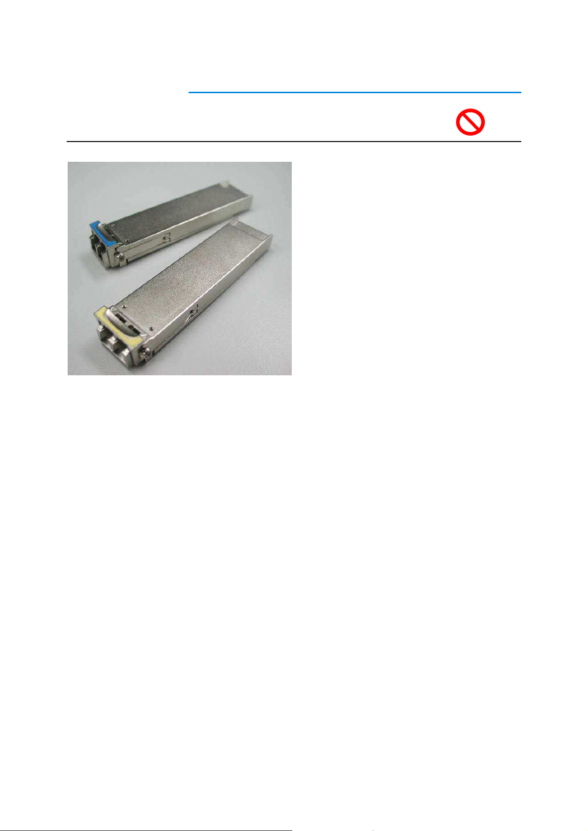
Description
The AXM752 is a hot pluggable 10Gbps
small-form-factor transceiver module integrated
with the high performance un-cooled 1310nm
EML-based transmitter, high sensitivity PIN
receiver and signal conditioner for 10Gbps
Ethernet applications that support link-distance
up to 10km over standard SMF. It is compliant
with the 10Gbps Ethernet IEEE 802.3ae
standard and the INF-8077i XFP Multi-source
Agreement (MSA).
The AXM752 is designed to be compliant with
INF-8077i XFP Multi-source Agreement (MSA)
with five digital monitoring functions:
Temperature, Vcc, Tx optical power, TX laser
bias current and RX received optical power.
Application
10G LAN switch
10G Ethernet switch/router
10G Fiber channel
10 Gigabit FC 10.5 Gb/s
10 Gigabit Ethernet 10.3 Gb/s
Performance
AXM752 data link up to 10km in 9/125um single
mode fiber.
1 Revision: 0A
Page 3
Temperature
Ambient Humidity
AXM752
1. Absolute Maximum Ratings
Parameter Symbol Min Typ Max Units Notes
Storage Temperature TS -40 85 °C
Storage Ambient Humidity
+5V Power Supply V
+3.3V Power Supply V
HA 5 90 %
0 6.0 V
CC5
0 3.6 V
CC3
2. Recommended Operating Conditions
Parameter Symbol Min Typ Max Units Notes
Operating Case
TC 0 70 °C
HA 5 85 % [1]
+3.3V Power Supply V
+5V Power Supply V
+3.3V Supply Current I
+5V Supply Current I
3.135 3.3 3.465 V
CC3
4.75 5 5.25 V
CC5
300 500 mA
VCC3
200 250 mA
VCC5
Total Power Dissipation PD 2.0 2.5 W
Differential TX Data Input TD+ - TD- 150 500 1000 mVp-p
[2,3]
Differential RX Data Output RD+ - RD- 500 650 800 mVp-p
Notes:
1. Non-condensing
2. The data rate of input data is 10.3125Gb/s
3. Input voltage swing (differential) measured peak-to-peak
4. Output voltage swing (differential) measured peak-to-peak
[4]
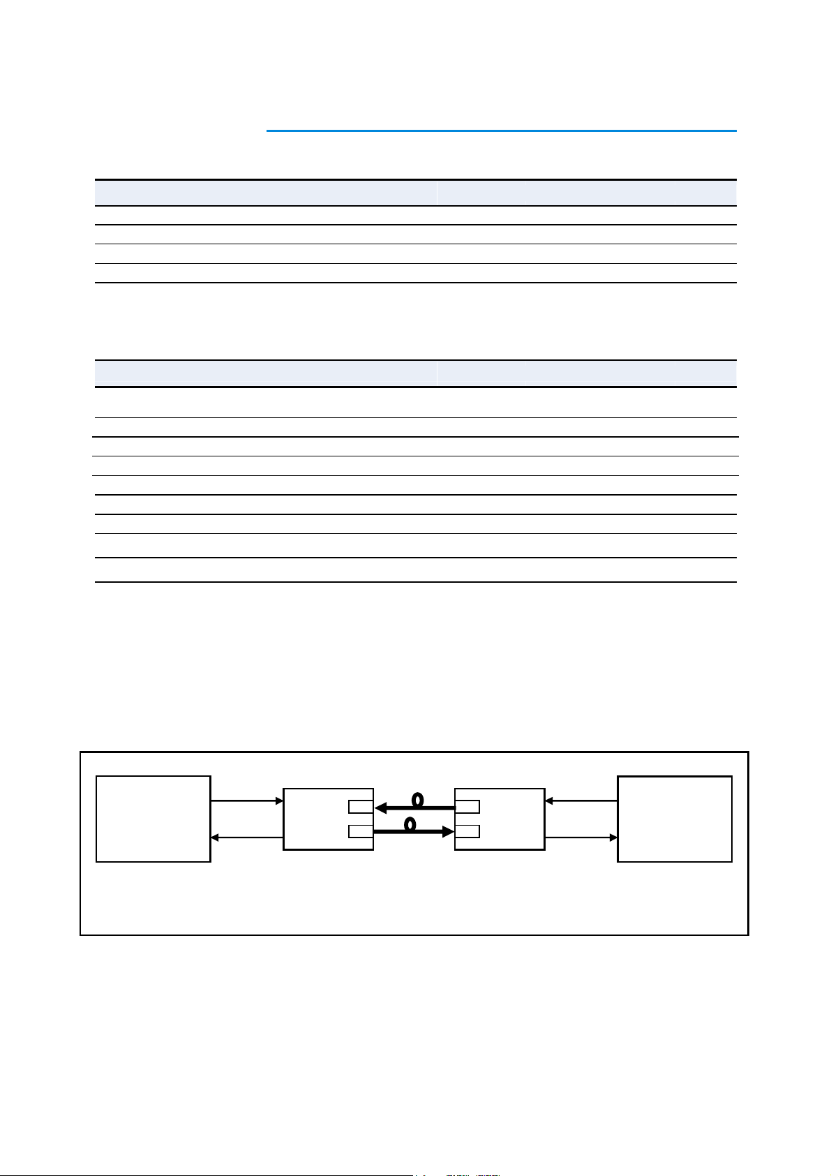
ASIC / SerDes
XFP
10Gbps optical signal 10Gbps XFI electrical signal 10Gbps XFI electrical signal
Application Block Diagram
2 Revision: 0A
XFP
ASIC / SerDes
Page 4
Amplitude
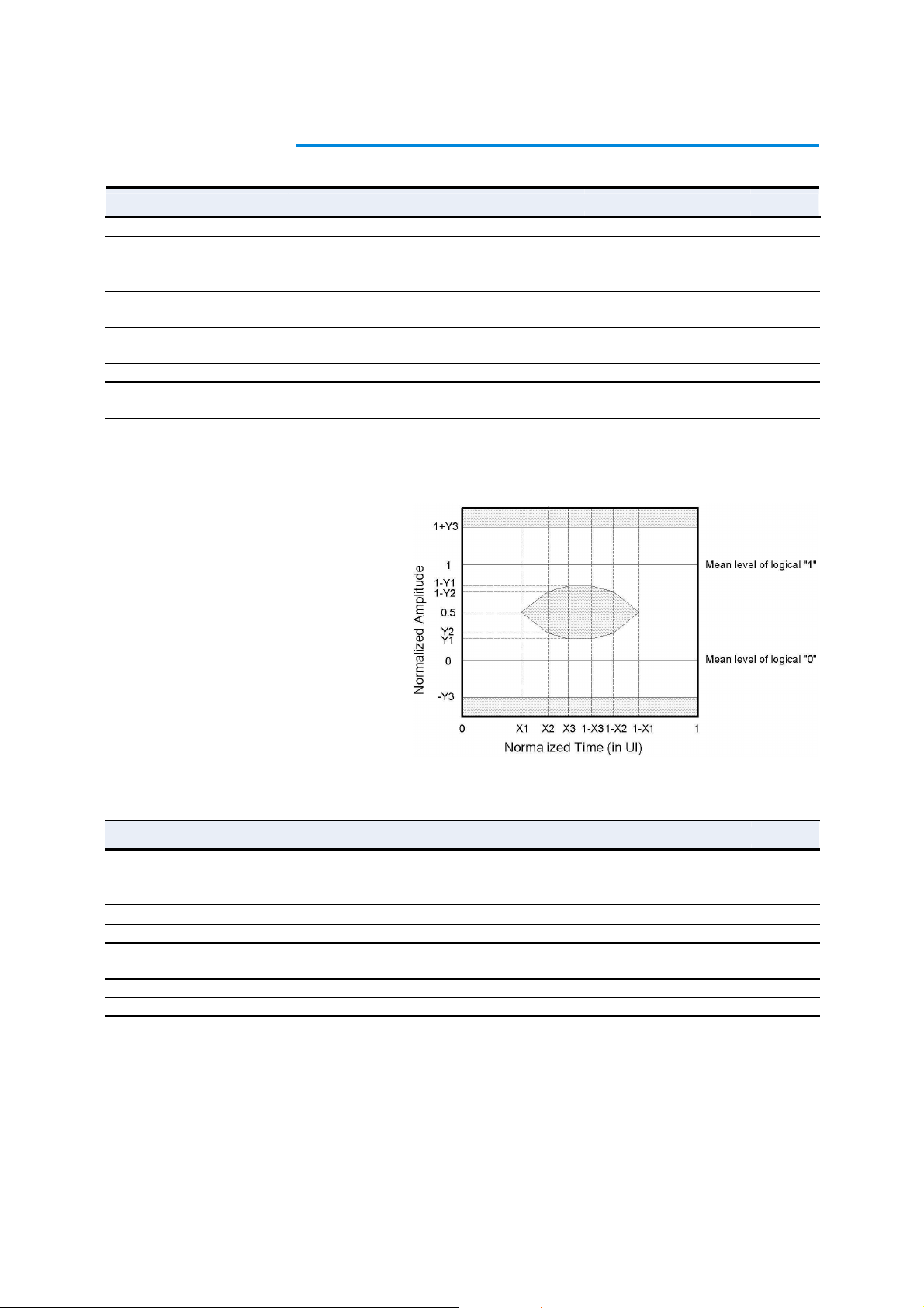
3. Optical Transmitter Characteristics
Parameter Symbol Min Typ Max Units Notes
Signaling speed (nominal)
Signaling speed variation
from nominal
Center Wavelength
Side Mode Suppression
Ratio
Optical Modulaion
Extinction Ratio ER 3.5 dB
Transmitter eye mask definition
{X1, X2, X3, Y1, Y2, Y3}
Notes:
1. Even if the TDP < 1 dB, the OMA (min) must exceed this value.
R 10.3125 Gb/s
λ
SMSR 30 dB
OMA -5.2 dBm
(TC=0 ºC to 70 ºC)
±100
1260 1355 nm
{0.25, 0.40, 0.45, 0.25, 0.28, 0.40}
Transmitter eye mask definition
AXM752
ppm
4. Optical Receive Characteristics
Parameter Symbol Min Typ Max Units Notes
Signaling speed (nominal)
Signaling speed variation
from nominal
Center Wavelength
Overload PO 0.5 dBm
Receiver sensitivity in
OMA
LOS De-assert LOSD -18 dBm
LOS Assert LOSA -30 dBm
Notes:
1. Measured with test signal for BER = 10
Ts 10.3125 Gb/s
λ
RSO -12.6 dBm [1]
(TC=0 ºC to 70 ºC)
1260 1355 nm
-12
.
3 Revision: 0A
±100
ppm
Page 5
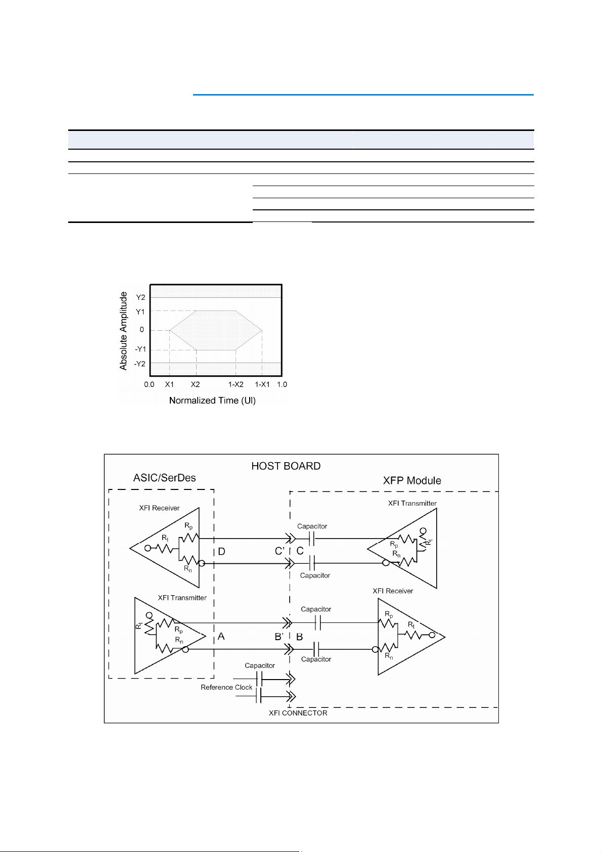
AXM752
5. XFI Module Receiver Output Jitter Specifications at C’
Parameter – C’ Symbol Min Typ Max Units Notes
Deterministic Jitter DJ 0.18 UI (p-p) [1]
Total Jitter TJ 0.34 UI (p-p) [1]
X1 0.17 UI
Eye Mask
Notes:
1. Includes jitter transferred from the optical receiver during any valid operational input condition.
XFI Module Receiver Differential Output Compliance Mask
X2 0.42 UI
Y1 170 mV
Y2 425 mV
XFI Termination and AC Coupling
4 Revision: 0A
Page 6
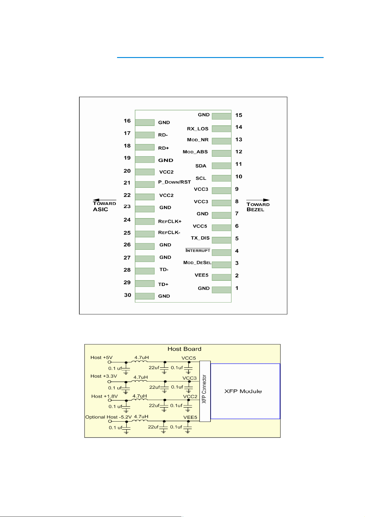
6. Pin Description
AXM752
XFP Host Board Connector Pad Layout (Top View)
Recommended Host Board Supply Filtering Network
5 Revision: 0A
Page 7

13
14
15
Module Electrical Pin Function Definition
AXM752
Pin
1 GND Module Ground
2 VEE5 Optional -5.2V Power Supply --Not Required
3 LVTTL-I Mod_DeSel
4 LVTTL-O Interrupt Bar
5 LVTTL-I TX_DIS Transmitter Disable; Turns off transmitter laser output
6 VCC5 +5V Power Supply
7 GND Module Ground
8 VCC3 +3.3V Power Supply
9 VCC3 +3.3V Power Supply
10 LVTTL-I/O SCL 2-Wire Serial Interface Clock [1]
11 LVTTL-I/O SDA 2-Wire Serial Interface Data Line [1]
12 LVTTL-O Mod_Abs Indicates Module is not present. Grounded in the Module [1]
16
17
18
19
20
21
22
23
24
25
26
27
28
29
30
Notes:
1. Module ground pins Gnd are isolated from the module case and chassis ground within the module.
2. Shall be pulled up with 4.7K-10Kohms to a voltage between 3.15V and 3.45V on the host board.
Logic Symbol Name/Description Note
Module De-select; When held low allows module to respond to
2-wire serial interface
Interrupt Bar; Indicates presence of an important condition
which can be read over the 2-wire serial interface
LVTTL-O Mod_NR Module Not Ready; Indicating Module Operational Fault [1]
LVTTL-O RX_LOS Receiver Loss Of Signal Indicator [1]
GND Module Ground
GND Module Ground
CML-O RD- Receiver Inverted Data Output
CML-O RD+ Receiver Non-Inverted Data Output
GND Module Ground
VCC2 +1.8V Power Supply --Not Required
Power down; When high, requires the module to limit power
LVTTL-I P_Down/RST
VCC2 +1.8V Power Supply --Not Required
GND Module Ground
PECL-I RefCLK-
PECL-I RefCLK+
GND Module Ground
GND Module Ground
CML-I TD- Transmitter Inverted Data Input
CML-I TD+ Transmitter Non-Inverted Data Input
GND Module Ground
consumption to 1.5W or below. 2-Wire serial interface must be
functional in the low power mode.
Reference Clock Non-Inverted Input, AC coupled on the host board,
Not required
Reference Clock Inverted Input, AC coupled on the host board,
Not required
[1]
6 Revision: 0A
Page 8

AXM752
7. Low Speed Electrical Hardware Pins
In addition to the 2-wire serial interface the XFP module has the following low speed pins for control and status:
‧ Mod_NR
‧ Mod_DeSel
‧ Interrupt
‧ TX_DIS
‧ Mod_ABS
‧ RX_Los
‧ P_Down/RST.
1 MOD_NR
The Mod_NR is an output pin that when High, indicates that the module has detected a condition that renders
transmitter and or receiver data invalid, shall consist of logical OR of the following signals:
‧ Transmit Signal Conditioner Loss of Lock
‧ Transmitter Laser Fault
‧ Receiver Signal Conditioner Loss of Lock
2 MOD_DESEL
The Mod_DeSel is an input pin. When held Low by the host, the module responds to 2-wire serial communication
commands. The Mod_DeSel allows the use of multiple XFP modules on a single 2-wire interface bus.
When the Mod_DeSel pin is “High”, the module shall not respond to or acknowledge any 2-wire interface
communication from the host. Mod_DeSel pin must be pulled to VCC3 in the module.
In order to avoid conflicts, the host system shall not attempt 2-wire interface communications within the Mod_DeSel
assert time after any XFP modules are deselected. Similarly, the host must wait at least for the period of the
Mod_DeSel deassert time before communicating with the newly selected module. The assertion and de-assertion
periods of different modules may overlap as long as the above timing requirements are met.
3 INTERRUPT
Interrupt is an output pin. When “Low”, indicates possible module operational fault or a status critical to the host
system. The Interrupt pin is an open collector output and must be pulled up to Host_Vcc the host board.
4 TX_DIS
TX_DIS is an input pin. When TX_DIS is asserted High, the XFP module transmitter output must be turned off. The
TX_DIS pin must be pulled up to VCC3 in the XFP module.
5 MOD_ABS
Mod_ABS is pulled up to Host_Vcc on the host board and grounded in the XFP module. Mod_ABS is then asserted
“High” when the XFP module is physically absent from a host slot.
6 RX_LOS
The RX_LOS when High indicates insufficient optical power for reliable signal reception. The RX_LOS pin is an open
collector output and must be pulled up to Host_Vcc on the host board.
7 Revision: 0A
Page 9

AXM752
7 P_DOWN/RST
This is a multifunction pin for module Power Down and Reset. The P_Down/RST pin must be pulled up to VCC3 in the
XFP module.
7.1 POWER DOWN FUNCTION
The P_Down pin, when held High by the host, places the module in the standby (Low Power) mode with a maximum
power dissipation of 1.5W.
7.2 RESET FUNCTION
The negative edge of P_Down/RST signal initiates a complete module reset.
3. Shall be pulled up with 4.7K-10Kohms to a voltage between 3.15V and 3.45V on the host board.
Notes:
8 Revision: 0A
Page 10

8. Memory Map of Management Interface
AXM752
The lower memory table (Byte 0~127) is for digital diagnostics and control functions. Besides, it has
been allocated three upper memory tables for serial ID, user writable and vendor specific functions. The
detail memory content is listed as following table.
9 Revision: 0A
Page 11

AXM752
9. EEPROM Serial ID Memory Contents (2-Wire Address A0h)
Address Hex ASCII Address Hex ASCII Address Hex ASCII
128 06 171 37 7 214 DC
129 50 172 35 5 215 DC
130 07 173 32 2 216 DC
131 40 174 20 217 DC
132 00 175 20 218 DC
133 00 176 20 219 DC
134 00 177 20 220 08
135 00 178 20 221 60
136 00 179 20 222 67
137 00 180 20 223 Note 4
138 00 181 20 224 VS Note 5
139 90 182 20 225 VS
140 64 183 20 226 VS
141 68 184 41 227 VS
142 0A 185 20 228 VS
143 00 186 66 3 229 VS
144 00 187 58 230 VS
145 00 188 0F 231 VS
146 00 189 A0 232 VS
147 60 190 46 233 VS
148 4E N 191 Note 1 234 VS
149 45 E 192 7D 235 VS
150 54 T 193 96 236 VS
151 47 G 194 55 237 VS
152 45 E 195 00 238 VS
153 41 A 196 SN Note 2 239 VS
154 52 R 197 SN 240 VS
155 20 198 SN 241 VS
156 20 199 SN 242 VS
157 20 200 SN 243 VS
158 20 201 SN 244 VS
159 20 202 SN 245 VS
160 20 203 SN 246 VS
161 20 204 SN 247 VS
162 20 205 SN 248 VS
163 20 206 SN 249 VS
164 C1 207 SN 250 VS
165 00 208 SN 251 VS
166 06 209 SN 252 VS
167 6E 210 SN 253 VS
168 41 A 211 SN 254 VS
169 58 X 212 DC Note 3 255 VS
170 4D M 213 DC
Notes:
1) CC_BASE : Check code for Base ID Fields (address 120~190)
2) Vendor SN (address 196–211)
3) Date Code (address 212–219)
CC_EXT : Check code for Extended ID Fields (address 192~222)
4)
5) Address 224~255 is reserved for vendor specific EEPROM
10 Revision: 0A
Page 12

10. Digital Diagnostic Monitoring Interface
Alarm and Warning Thresholds (2-Wire Address A0h)
AXM752
Address
01 1
02–03 2
04–05 2
06–07 2
08–09 2
10–17 8
18–19 2
20–21 2
22–23 2
24–25 2
26–27 2
28–29 2
30–31 2
32–33 2
34–35 2
36–37 2
38–39 2
40–41 2
42–43 2
44–45 2
46–47 2
48–49 2
50–51 2
52–53 2
54–55 2
56–57 2
96 1
97 1
98–99 10
100
101
102
103
104
105
106
107
108
109
#
Bytes
1
1
1
1
1
1
1
1
1
1
Name Value (Dec.) Unit
Signal Conditioner Control
Temp High Alarm 90
Temp Low Alarm
Temp High Warning 85
Temp Low Warning
Reserved
Bias High Alarm
Bias Low Alarm
Bias High Warning
Bias Low Warning
TX Power High Alarm
TX Power Low Alarm
TX Power High Warning
TX Power Low Warning
RX Power High Alarm
RX Power Low Alarm
RX Power High Warning
RX Power Low Warning
AUX 1 High Alarm
AUX 1 Low Alarm
AUX 1 High Warning
AUX 1 Low Warning
AUX 2 High Alarm
AUX 2 Low Alarm
AUX 2 High Warning
AUX 2 Low Warning
Temperature MSB
Temperature LSB
Reserved
TX Bias MSB
TX Bias LSB
TX Power MSB
TX Power LSB
RX Power MSB
RX Power LSB
AUX 1 MSB(5V)
AUX 1 LSB (5V)
AUX 2 LSB (3.3V)
AUX 2 LSB (3.3V)
Notes:
1) P: Operating optical power of transmitter at room temperature
2) Iop: Operating bias current of transmitter at room temperature
-10
-5
Iop+60 mA
Iop-25 mA
Iop+55 mA
Iop-20 mA
P+3
P–3
P+2
P–2
-3
-23
-5
-21
5.5
4.5
5.3
4.7
3.6
3.0
3.5
3.1
℃
mA
dBm
dBm
Volt
Volt
11 Revision: 0A
Page 13

General State/ Control Bits
Byte Bit Name Description
1 0
1 1
1 2
1 4-7
110 7 Tx Disable State Digital state of the Tx disable input pin
110 6 Optional Soft TX Disable Read/ Write bit that allow software disable of laser
110 5 MOD_NR State Digital state of Module Not Ready
110 4 P-Down State Digital state Power Down
110 3
110 2
110 1 LOS Digital state of the LOS output pin.
110 0 Data_Not_Ready Digital state of Data_Not_Ready
111 7
111 6
111 5
111 4
111 3
119–122
123–126
127 All
Signal Conditioner Control
XFI Loopback
Lineside Loopback
Data Rate Control
Soft P_Down
_____________
Interrupt
TX_NR State
TX_Fault State
TX_CDR not Locked
RX_NR State
RX_CDR not Locked
New Password Entry
All
Password Entry
All
Table Select
Default value of this bit is 0
XFI loopback enable when this bit set to 1
Not Implement
Default setting is 10.3Gbps
Software Power Down
Interrupt Bar State
Digital state of Tx Not Ready State
Digital state of Tx Fault State
Digital state of Tx CDR not Locked
Digital state of Rx Not Ready
Digital state of Rx CDR not Locked
Location for Entry of New Optional Password
Location for Entry of Optional Password
Entry Location for Table Select Byte
AXM752
Optional Set of Alarm and Warning
Byte Bit Name Description
80 7 Temp High Alarm Set when internal temperature exceeds high alarm level
80 6 Temp Low Alarm Set when internal temperature is below low alarm level
80 5 Reserved
80 4 Reserved
80 3 Tx Bias High Alarm Set when Tx Bias current exceeds high alarm level
80 2 Tx Bias Low Alarm Set when Tx Bias current is below low alarm level
80 1 Tx Power High Alarm Set when Tx output power exceeds high alarm level
80 0 Tx Power Low Alarm Set when Tx output power is below low alarm level
81 7 Rx Power High Alarm Set when received power exceeds high alarm level
81 6 Rx Power Low Alarm Set when received power is below low alarm level
81 5 AUX1 High Alarm Set when internal 5V supply voltage exceeds high alarm level
81 4 AUX1 Low Alarm Set when internal 5V supply voltage is below low alarm level
81 3 AUX2 High Alarm
81 2 AUX2 Low Alarm
81 1 Reserved
81 0 Reserved
82 7 Temp High Warning Set when internal temperature exceeds high warning level
82 6 Temp Low Warning Set when internal temperature is below low warning level
82 5 Reserved
82 4 Reserved
82 3 Tx Bias High Warning Set when Tx Bias current exceeds high warning level
82 2 Tx Bias Low Warning Set when Tx Bias current is below low warning level
82 1 Tx Power High Warning Set when Tx output power exceeds high warning level
82 0 Tx Power Low Warning Set when Tx output power is below low warning level
Set when internal 3.3V supply voltage exceeds high alarm
level
Set when internal 3.3V supply voltage is below low alarm
level
12 Revision: 0A
Page 14

83 7 Rx Power High Warning Set when received power exceeds high warning level
83 6 Rx Power Low Warning Set when received power is below low warning level
83 5 AUX1 High Warning
83 4 AUX1 Low Warning
83 3 AUX2 High Warning
83 2 AUX2 Low Warning
83 1 Reserved
83 0 Reserved
Set when internal 5V supply voltage exceeds high warning
level
Set when internal 5V supply voltage is below low warning
level
Set when internal 3.3V supply voltage exceeds high warning
level
Set when internal 3.3V supply voltage is below low warning
level
AXM752
13 Revision: 0A
Page 15

11. Mechanical Outline Dimensions
Transmitter Wavelength / Application Latch Color Identifier
1310nm / LR
AXM752
Blue
AXM752
Single Mode/1310nm 10Gbps
10GBase-LR up to 10km
Class 1 Laser Product
Complies with
21 CFR 1040.10
and 1040.11
Made in Taiwan
272-10320-02
R
14 Revision: 0A
Page 16

Component Recognition for Information
11. Regulatory Compliance
Feature Reference Performance
AXM752
Electromagnetic Interference
(EMI)
Radio Frequency
Electromagnetic Field
Electrostatic Discharge to the
Duplex LC Receptacle
Electrostatic Discharge to the
Electrical Pins
Eye Safety US FDA CDRH AEL Class 1
Component Recognition
FCC CRF 47, Part15 Class B
EN 55022 Class B (CISPR 22A)
EN 61000-4-3
IEC 61000-4-3
EN 61000-4-2
IEC 61000-4-2
IEC 801.2
MIL-STD-883E Method 3015.7
Underwriters Laboratories and
Canadian Standards Association Joint
Technology Equipment Including
Electrical Business Equipment
(1) Satisfied with electrical
characteristics of product
spec.
(2) No physical damage
UL File # E239394
15 Revision: 0A
Page 17

Appendix A. Document Revision
Version No.
S0 2006-04-25 Preliminary datasheet for RoHS version
S1 2006-08-25 Update Digital Diagnostic Memory Map contents
S2 2007-10-02 Modify the dimension of label
0A 2007-11-09 Modify the Byte 165~167 of A0h
Date Description
AXM752
16 Revision: 0A
Page 18

© 2008 NETGEAR, Inc. NETGEAR, the NETGEAR Logo, NETGEAR Digital Entertainer Logo, Connect with Innovation,
FrontView, IntelliFi, PowerShift, ProSafe, RAIDar, RAIDiator, X-RAID, RangeMax, ReadyNAS and Smart Wizard are trademarks of
NETGEAR, Inc. in the United States and/or other countries. Other brand names mentioned herein are for identification purposes
only and may be trademarks of their respective holder(s). Information is subject to change without notice. All rights reserved.
D-AXM752-0
 Loading...