

Page 1

User's Manual
32-bit V850 ZigBee™ PRO
Gateway Development
Platform
Document No. U19026EE3V0UM00
Date published October 2009
© NEC Electronics 2009
Printed in Germany
Page 2

Legal Notes
•
The information in this document is current as of July, 2008. The
information is subject to change without notice. For actual
design-in, refer to the latest publications of NEC Electronics
data sheets or data books, etc., for the most up-to-date
specifications of NEC Electronics products. Not all products
and/or types are available in every country. Please check with
an NEC Electronics sales representative for availability and
additional information.
• No part of this document may be copied or reproduced in any form
or by any means without the prior written consent of NEC
Electronics. NEC Electronics assumes no responsibility for any
errors that may appear in this document.
• NEC Electronics does not assume any liability for infringement of
patents, copyrights or other intellectual property rights of third
parties by or arising from the use of NEC Electronics products listed
in this document or any other liability arising from the use of such
products. No license, express, implied or otherwise, is granted under
any patents, copyrights or other intellectual property rights of NEC
Electronics or others.
• Descriptions of circuits, software and other related information in this
document are provided for illustrative purposes in semiconductor
product operation and application examples. The incorporation of
these circuits, software and information in the design of a customer's
equipment shall be done under the full responsibility of the customer.
NEC Electronics assumes no responsibility for any losses incurred
by customers or third parties arising from the use of these circuits,
software and information.
• While NEC Electronics endeavors to enhance the quality, reliability
and safety of NEC Electronics products, customers agree and
acknowledge that the possibility of defects thereof cannot be
eliminated entirely. To minimize risks of damage to property or injury
(including death) to persons arising from defects in NEC Electronics
products, customers must incorporate sufficient safety measures in
their design, such as redundancy, fire-containment and anti-failure
features.
• NEC Electronics products are classified into the following three
quality grades: "Standard", "Special" and "Specific".
• The "Specific" quality grade applies only to NEC Electronics
products developed based on a customer-designated "quality
assurance program" for a specific application. The recommended
applications of an NEC Electronics product depend on its quality
grade, as indicated below. Customers must check the quality grade
of each NEC Electronics product before using it in a particular
application.
"Standard": Computers, office equipment, communications
equipment, test and measurement equipment, audio and visual
equipment, home electronic appliances, machine tools, personal
electronic equipment and industrial robots.
"Special": Transportation equipment (automobiles, trains, ships,
etc.), traffic control systems, anti-disaster systems, anti-crime
2
User's Manual U19026EE3V0UM00
Page 3

systems, safety equipment and medical equipment (not specifically
designed for life support).
"Specific": Aircraft, aerospace equipment, submersible repeaters,
nuclear reactor control systems, life support systems and medical
equipment for life support, etc.
The quality grade of NEC Electronics products is "Standard" unless otherwise
expressly specified in NEC Electronics data sheets or data books, etc. If
customers wish to use NEC Electronics products in applications not intended by
NEC Electronics, they must contact an NEC Electronics sales representative in
advance to determine NEC Electronics' willingness to support a given application.
(Note)
(1) "NEC Electronics" as used in this statement means NEC Electronics
Corporation and also includes its majority-owned subsidiaries.
(2) "NEC Electronics products" means any product developed or manufactured
by or for NEC Electronics (as defined above).
User's Manual U19026EE3V0UM00
3
Page 4

Regional Information
Some information contained in this document may vary from country to country. Before
using any NEC product in your application, please contact the NEC office in your country
to obtain a list of authorized representatives anddistributors. They will verify:
• Device availability
• Ordering information
• Product release schedule
• Availability of related technical literature
• Development environment specifications (for example, specifications for
• Network requirements
In addition, trademarks, registered trademarks, export restrictions, and otherlegal
issues may also vary from country to country.
NEC Electronics Corporation
1753, Shimonumabe, Nakahara-ku,
Kawasaki, Kanagawa 211-8668, Japan
Tel: 044 4355111
http://www.necel.com/
[America]
NEC Electronics America, Inc.
2880 Scott Blvd.
Santa Clara, CA 95050-2554,
U.S.A.
Tel: 408 5886000
http://www.am.necel.com/
third-party tools and components, host computers, power plugs, AC
supply voltages, and so forth)
[Europe]
NEC Electronics (Europe) GmbH
Arcadiastrasse 10
40472 Düsseldorf, Germany
Tel: 0211 65030
http://www.eu.necel.com/
United Kingdom Branch
Cygnus House, Sunrise Parkway
Linford Wood, Milton Keynes
MK14 6NP, U.K.
Tel: 01908 691133
Succursale Française
9, rue Paul Dautier, B.P. 52
78142 Velizy-Villacoublay Cédex
France
Tel: 01 30675800
Tyskland Filial
Täby Centrum
Entrance S (7th floor)
18322 Täby, Sweden
Tel: 08 6387200
Filiale Italiana
Via Fabio Filzi, 25/A
20124 Milano, Italy
Tel: 02 667541
Branch The Netherlands
Steijgerweg 6
5616 HS Eindhoven,
The Netherlands
Tel: 040 2654010
[Asia & Oceania]
NEC Electronics (China) Co., Ltd
7th Floor, Quantum Plaza, No. 27
ZhiChunLu Haidian District,
Beijing 100083, P.R.China
Tel: 010 82351155
http://www.cn.necel.com/
NEC Electronics Shanghai Ltd.
Room 2511-2512, Bank of China
Tower,
200 Yincheng Road Central,
Pudong New Area,
Shanghai 200120, P.R. China
Tel: 021 58885400
http://www.cn.necel.com/
NEC Electronics Hong Kong Ltd.
12/F., Cityplaza 4,
12 Taikoo Wan Road, Hong Kong
Tel: 2886 9318
http://www.hk.necel.com/
NEC Electronics Taiwan Ltd.
7F, No. 363 Fu Shing North Road
Taipei, Taiwan, R.O.C.
Tel: 02 27192377
NEC Electronics Singapore Pte. Ltd.
238A Thomson Road,
#12-08 Novena Square,
Singapore 307684
Tel: 6253 8311
http://www.sg.necel.com/
NEC Electronics Korea Ltd.
11F., Samik Lavied’or Bldg., 720-2,
Yeoksam-Dong, Kangnam-Ku, Seoul,
135-080, Korea Tel: 02-558-3737
http://www.kr.necel.com/
4
User's Manual U19026EE3V0UM00
Page 5

Table of Contents
Chapter 1 V850 ZigBee PRO Gateway Development Platform
.......................................................................... 7
1.1 Features of the TK-850/SG2+UZ ....................................................
1.2 Package Content .................................................................
1.3 System Requirements .............................................................
1.4 Complementary ZigBee™ Development Platform and Hardware ......................
7
7
8
8
Chapter 2 Sample Program .................................................
2.1 Operational Procedure for the TK-850/SG2+UZ .....................................
2.2 Operation Procedure with TK-78K0/KF2+UZ boards .................................
Chapter 3 Hardware specification ........................................
3.1 Terminal list ......................................................................
3.2 Switches and LED .................................................................
3.2.1 SW1, JP1 ................................................................ 22
3.2.2 SW2, SW3 ............................................................... 24
3.2.3 SW4 ..................................................................... 24
3.2.4 LED5 .................................................................... 24
3.2.5 LED1, LED2, LED3 and LED4 ............................................... 24
3.3 LAN Controller ....................................................................
3.3.1 Connection ............................................................... 25
3.3.2 Reset of LAN Controller .................................................... 26
3.3.3 Access to the LAN Controller ............................................... 26
3.4 Temperature Sensor ..............................................................
3.5 Power Supply .....................................................................
Chapter 4 TK-850/SG2+UZ Data .........................................
4.1 Parts Layout ......................................................................
4.2 RF Board connection figure ........................................................
10
10
14
19
19
22
25
26
26
28
28
29
Chapter 5 Programming the TK-850/SG2+UZ with WriteEZ1 ...
Chapter 6 V850 ZigBee Gateway Development Platform,
Installation and Operation ....................................
6.1 Hardware Installation ..............................................................
6.2 Software Installation ..............................................................
6.2.1 IAR Systems Embedded Workbench installation .............................. 36
6.2.2 GUI software WriteEZ1 for Flash Programming ............................... 37
6.2.3 Sample Program Installation ................................................ 37
6.3 USB Driver Installation ............................................................
6.3.1 Installation on Windows XP ................................................. 37
Chapter 7 IAR Sample Session ............................................
7.1 Sample Structure .................................................................
7.2 Project Loading ...................................................................
7.3 Sample Debug session using the TK interface .......................................
7.4 Generating a Hex file for Flash programming ........................................
User's Manual U19026EE3V0UM00
30
36
36
36
37
40
40
41
42
48
5
Page 6

Chapter 8 Sample Program .................................................
8.1 User configurable network Parameters .............................................
8.2 Libraries ..........................................................................
8.3 Embedded functions in Web Pages .................................................
8.4 System Initialization ...............................................................
50
50
50
50
52
Chapter 9 Schematic Diagram TK-850/SG2+UZ .....................
Chapter 10 Circuit Diagram of UZ2400 RF Board .....................
53
57
6
User's Manual U19026EE3V0UM00
Page 7

Chapter 1 V850 ZigBee PRO Gateway
Development Platform
The V850 ZigBeeTM PRO Gateway Development Platform is the NEC Electronics
32-bit starter kit specifically designed for the development of wireless networking
applications combined with Ethernet and Internet communications. The above
platform can be used to design and develop high-end wireless networking,
incorporating all the features of a fully compliant ZigBeeTM network. This
development platform also has Ethernet and Internet capability which can support
communications via WEB browser-based technology.
The development kit contains the TK-850/SG2+UZ evaluation board, which
includes the V850ES/SG2, a 32-bit single-chip microcontroller of NEC
Electronics, and the UZ2400 RF board of Uniband Electronic Corporation.
1.1 Features of the TK-850/SG2+UZ
Features of the TK-850/SG2+UZ CPU evaluation board are as follows.
Note
• The evaluation board used the NEC Electronics 32-bit single chip
microcontroller (µPD70F3281YGC). All of the ROM, RAM and
peripheral circuit are efficiently built in one chip on a single board.
• High-speed operation is realized via the 20 MHz internal clock.
• 32.768 kHz sub-clock standard equipment
• The high speed RAM: 32 KB and the flash memory 384 KB are built
into CPU chip.
• Hardware is ready to accommodate the 2.4 GHz transceiver UZ2400
RF board (Accordance with IEEE 802.15.4 ZigBeeTM Specifications
for Low Rate Wireless Personal Area Networks) made by Uniband
Electronic Corporation.
( http://www.ubec.com.tw/index.html)
• Attached antenna Titanis made by Gigaant
( http://www.gigaant.com)
• 17 I/O ports are equipped for expand use.
• On board temperature sensor S-8120C made by SII
( http://www.sii.co.jp)
• The board itself is quite and easy to handle; the CPU board size is
91 mm x 62 mm, and 103 mm x 62 mm when the RF transceiver
board is included.
Please inquire direct to the parts maker about specification of UZ2400 RF board,
antenna and temperature sensor.
1.2 Package Content
The V850 ZigBeeTM PRO Gateway Development Platform consists of one
TK-850/SG2+UZ development board and one 78K0_UZ_Stick which is
configured to act as Air Sniffer hardware. Also supplied is the unlimited security
User's Manual U19026EE3V0UM00
7
Page 8

Chapter 1 V850 ZigBee PRO Gateway Development Platform
dongle for the V850 ZigBeeTM PRO stack and ZigBeeTM PRO Software
Developers Kit (ZigBeeTM PRO SDK tools).
The following software is also supplied on the accompanying CDROM.
• IAR Embedded Workbench Kickstart edition 64KB code size limited
• WriteEZ1 Flash programming Software for the V850 microcontrollers
• IEEE 802.15.4 MAC libraries
• TCPIP libraries, Mail and Web application libraries
• Web Page Conversion Utility Program
• Sample Web to Wireless application program for the TK-850/SG2
+UZ board
• Compiled HEX file for remote TK-78K0/KF2+UZ wireless node
(hardware not supplied)
1.3 System Requirements
Host PC
Host Interface
Package Contents
Note
Trademarks
A PC supporting Windows 2000 or Windows XP for the IAR Systems Embedded
Workbench Kickstart edition and the V850 ZigBee™ PRO Gateway Development
Platform.
Pentium 200 MHz minimum, 128 MB of RAM, 256 colour display (1024 x 768),
mouse, CD ROM drive and 200 MB of disk space are required to install the tool
packages.
USB interface that enables communication based on USB (Version 1.1 or later)
Please verify that you have received all of the parts listed in the package contents
list attached to the V850 ZigBee™ PRO Gateway Development Platform. If any
parts are missing or seem to be damaged please contact the dealer from whom
you received your V850 ZigBee™ PRO Gateway Development Platform.
Updates for the IAR Embedded workbench for V850, documentation and/or
utilities for the V850 ZigBee™ PRO Gateway Development Platform if available
maybe downloaded from the NEC Electronics web pages at: http://
www.eu.necel.com/updates
IAR Embedded Workbench, visualSTATE, IAR MakeApp and C-SPY are
registered trademarks of IAR Systems AB. Microsoft and Windows are registered
trademarks of Microsoft Corporation.
Adobe and Acrobat Reader are registered trademarks of Adobe Systems
Incorporated.
All other product names are trademarks or registered trademarks of their
respective owners.
1.4 Complementary ZigBee™ Development Platform and Hardware
Other evaluation boards and hardware available to develop a ZigBeeTM network
from NEC Electronics:
•
ZigBeeTM Starter Kit
-
2 x 8-bit ZigBeeTM node boards TK-78K0/KF2+UZ
8
User's Manual U19026EE3V0UM00
Page 9

V850 ZigBee PRO Gateway Development Platform Chapter 1
- IEEE 802.15.4 MAC libraries
- Sample programs
- IAR Embedded Workbench Kickstart Version
- Flash programmer for 78K0
-
Article code 78K0-ZIGBEE-SK
•
ZigBeeTM Premium Development Kit for 78K0
-
4 x 8-bit ZigBeeTM node boards TK-78K0/KF2+UZ
-
8-Bit USB ZigBeeTM node programmed as Air Sniffer
- IEEE 802.15.4 MAC libraries
-
ZigBeeTM Stack
-
Unlimited ZigBeeTM license for the 78K0 family
- GUI Tools (SDK)
- Sample programs
- IAR Embedded Workbench Kickstart Version
- Flash programmer for 78K0
-
Article code 78K0-ZIGBEE-PREM
•
ZigBeeTM Premium Development Kit for 78K0R
-
4 x 16-bit ZigBeeTM node boards TK-78K0R/KG3+UZ
-
16-bit USB ZigBeeTM node programmed as Air Sniffer
- IEEE 802.15.4 MAC libraries
-
ZigBeeTM Stack
-
Unlimited ZigBeeTM license for the 78K0R family
- GUI Tools (SDK)
- Sample programs
- IAR Embedded Workbench Kickstart Version
-
Article code 78K0R-ZIGBEE-PREM
•
ZigBeeTM PRO Premium Development Kit for 78K0R
-
4 x 16-bit ZigBeeTM node boards TK-78K0R/KG3+UZ
-
16-bit USB ZigBeeTM node programmed as Air Sniffer
- IEEE 802.15.4 MAC libraries
-
ZigBeeTM Stack
-
Unlimited ZigBeeTM license for the 78K0R family
- GUI Tools (SDK)
- Sample programs
- IAR Embedded Workbench Kickstart Version
-
Article code 78K0R-ZIGBEEPRO-PREM
Additional single boards or modules can be purchased in case the customer
needs additional hardware for Premium or Gateway kits:
- TK-850/SG2+UZ-EE
- TK-78K0/KF2+UZ-EE
- 78K0_UZ_Stick-EE
- TK-78K0R/KG3+UZ-EE
- 78K0R_UZ_Stick-EE
User's Manual U19026EE3V0UM00
9
Page 10
Chapter 2 Sample Program
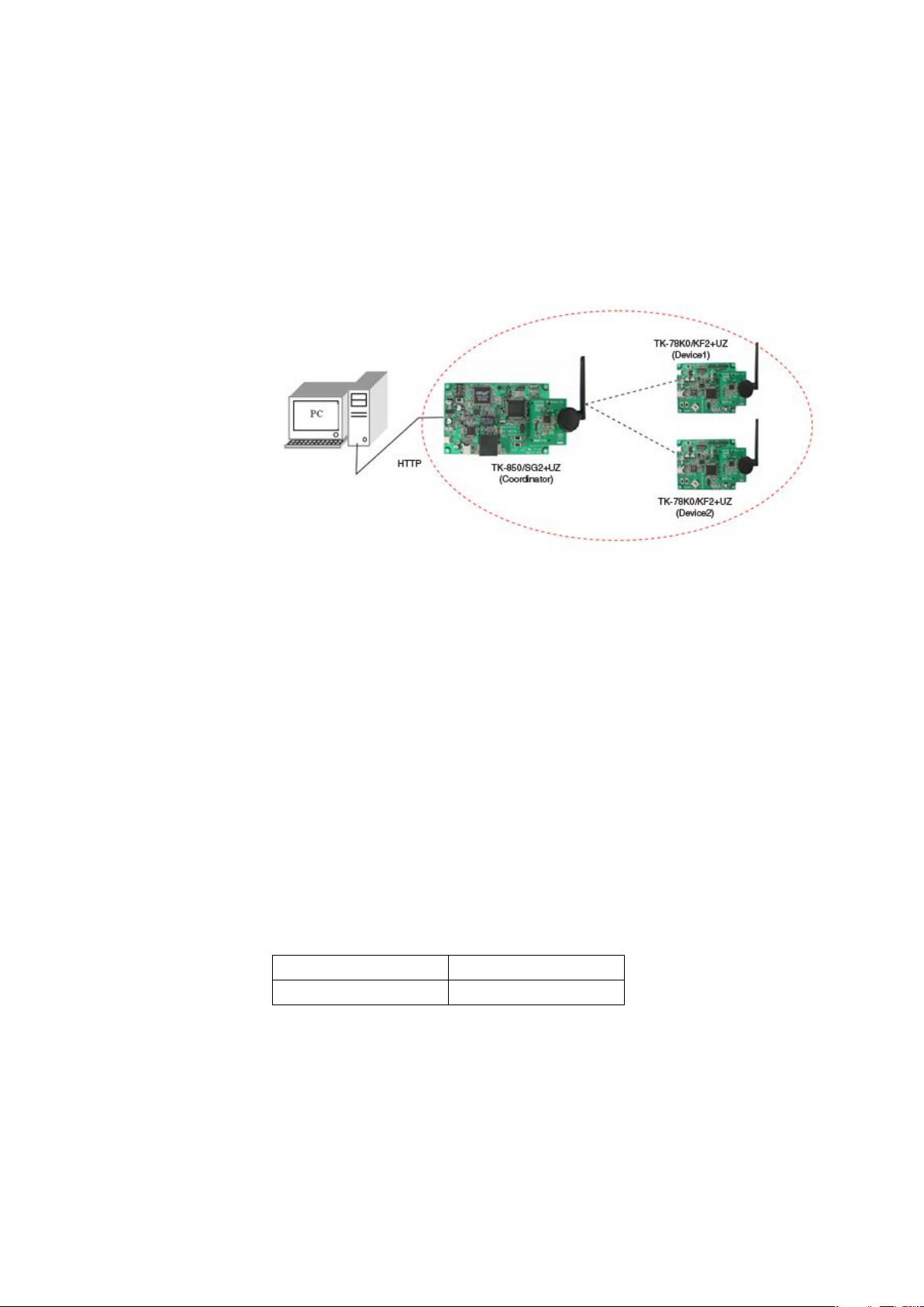
The sample program provided permits the user to set up the following network
where the TK-850/SG2+UZ board occupies the central position. The
TK-850/SG2+UZ is already pre-programmed with the "mac_app.hex" file which
utilises the following network configuration:
Figure 2-1 System Configuration
The sample application utilizes TCP/IP and HTTP communications on the
TK-850/SG2+UZ board, and wireless communications of IEEE 802.15.4, between
one TK-850/SG2+UZ board and up to 4 TK-78K0/KF2+UZ boards (not supplied).
The TK-850/SG2+UZ board is called “Coordinator” and the TK-78K0/KF2+UZ
boards “Devices”.
The following parts present firstly, the operation of the central board alone, and
then the operation with the addition of TK-78K0/KF2+UZ boards.
2.1 Operational Procedure for the TK-850/SG2+UZ
If you intend to execute the sample program without using the debugger, set the
mode switch as shown below, and then, make a hardware reset by pushing the
reset switch.
Table 2-1 Operation mode settings for the TK-850/SG2+UZ
SW1 – 1, 2, 3 and 4 OFF
SW1 – 5, 6, 7 and 8 X
Connect your PC to the TK-850/SG2+UZ board with a LAN cable. The LAN cable
should be a crossover cable if connected directly through to the PC or a straight
cable if utilising normal network connections.
10
Apply the power source to the TK-850/SG2+UZ board (batteries or powered
USB).
User's Manual U19026EE3V0UM00
Page 11
Sample Program Chapter 2
Some changes need to be made to your PC network settings: open [Control Panel]
-> [Network Connections] -> [Local Area Connections] -> [Properties] -> [TCP/IP]
-> [Properties] and set the following IP address and the subnet mask:
- IP address: 192.168.0.x.x can be any value between 1 to 99, or 101
to 25.
- Subnet mask: 255.255.255.0
Close the TCP/IP set up window.
Start you web browser, such as MS Internet Explorer.
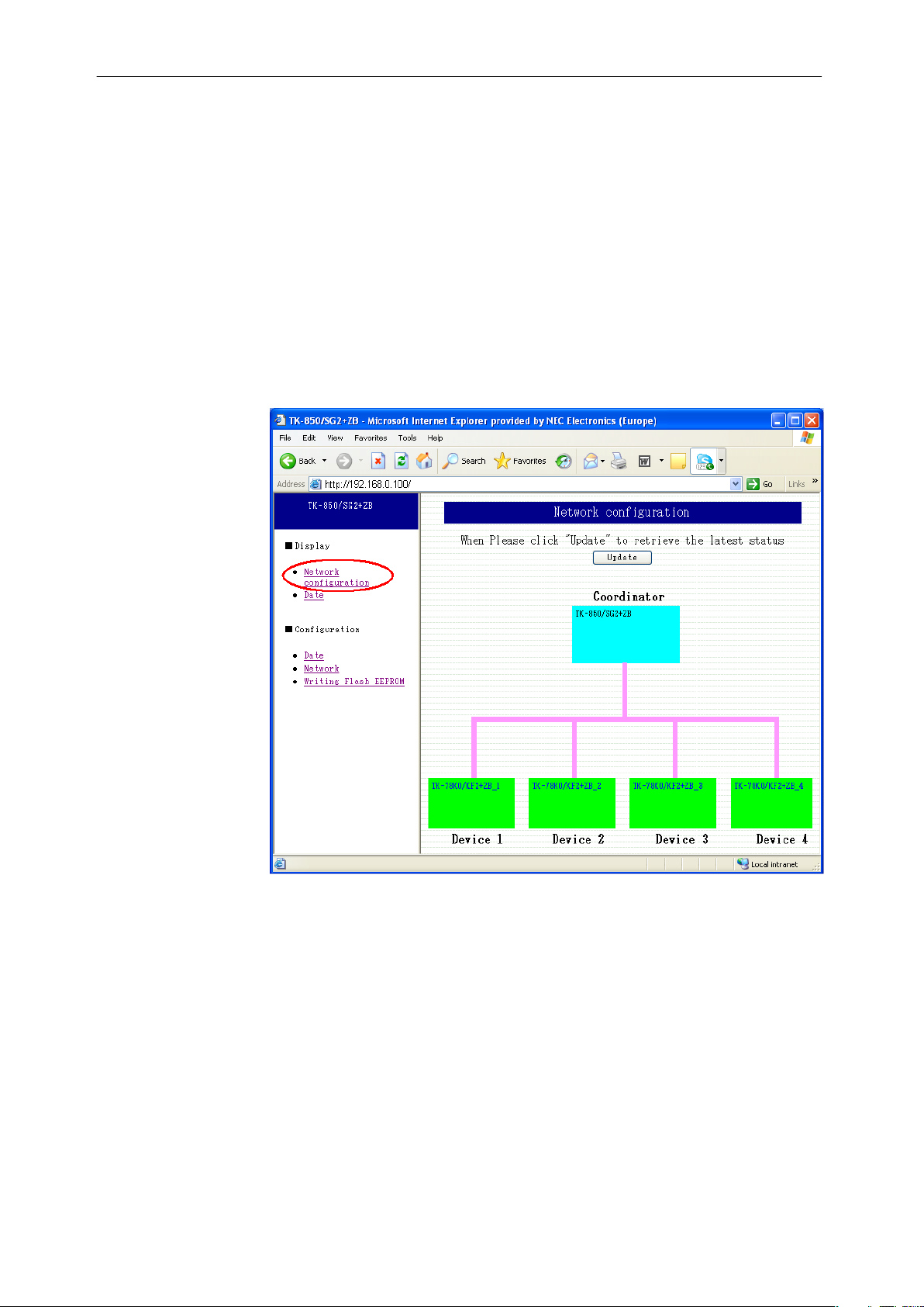
Connect your browser to “http://192.168.0.100”. You can modify the URL later
by going to [Configuration] -> [Network]
You should see the following image in your browser.
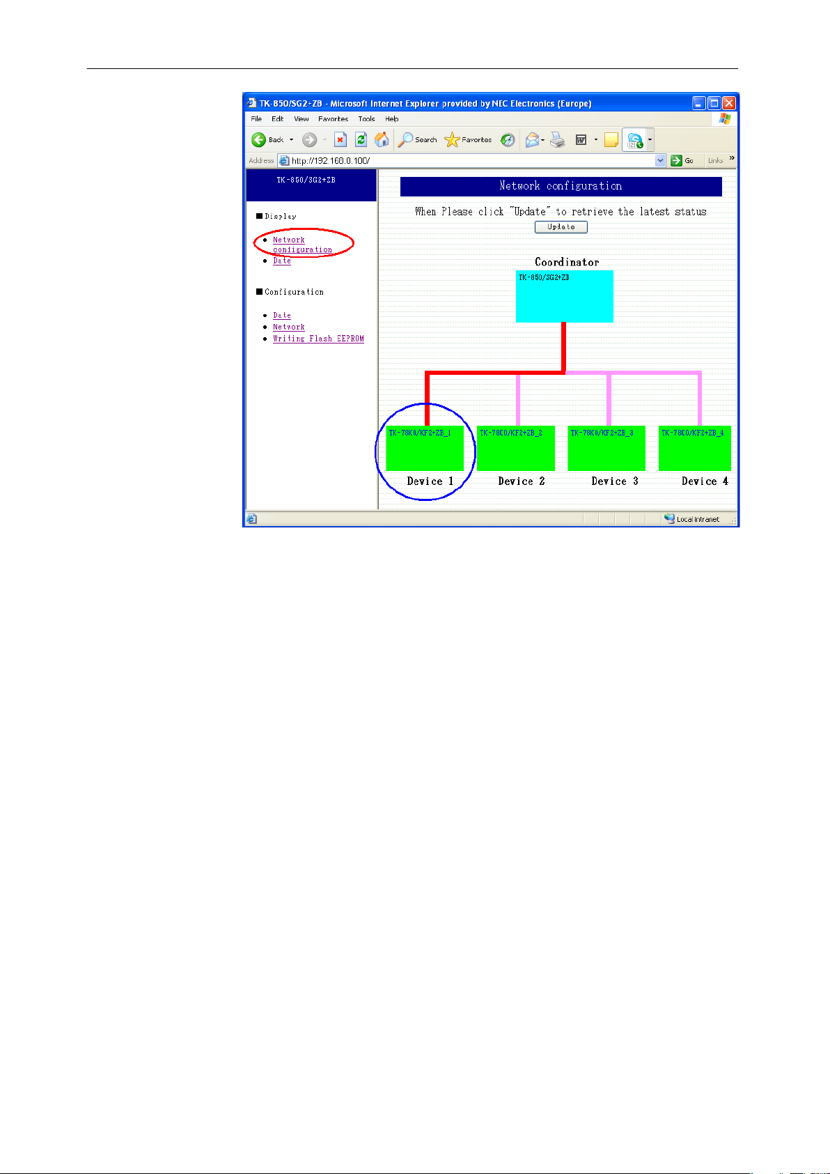
You can come back to this image, anytime if you select [Display] -> [Network
Configuration]. A pink line indicates a device is not connected.
Figure 2-2 Network configuration overview
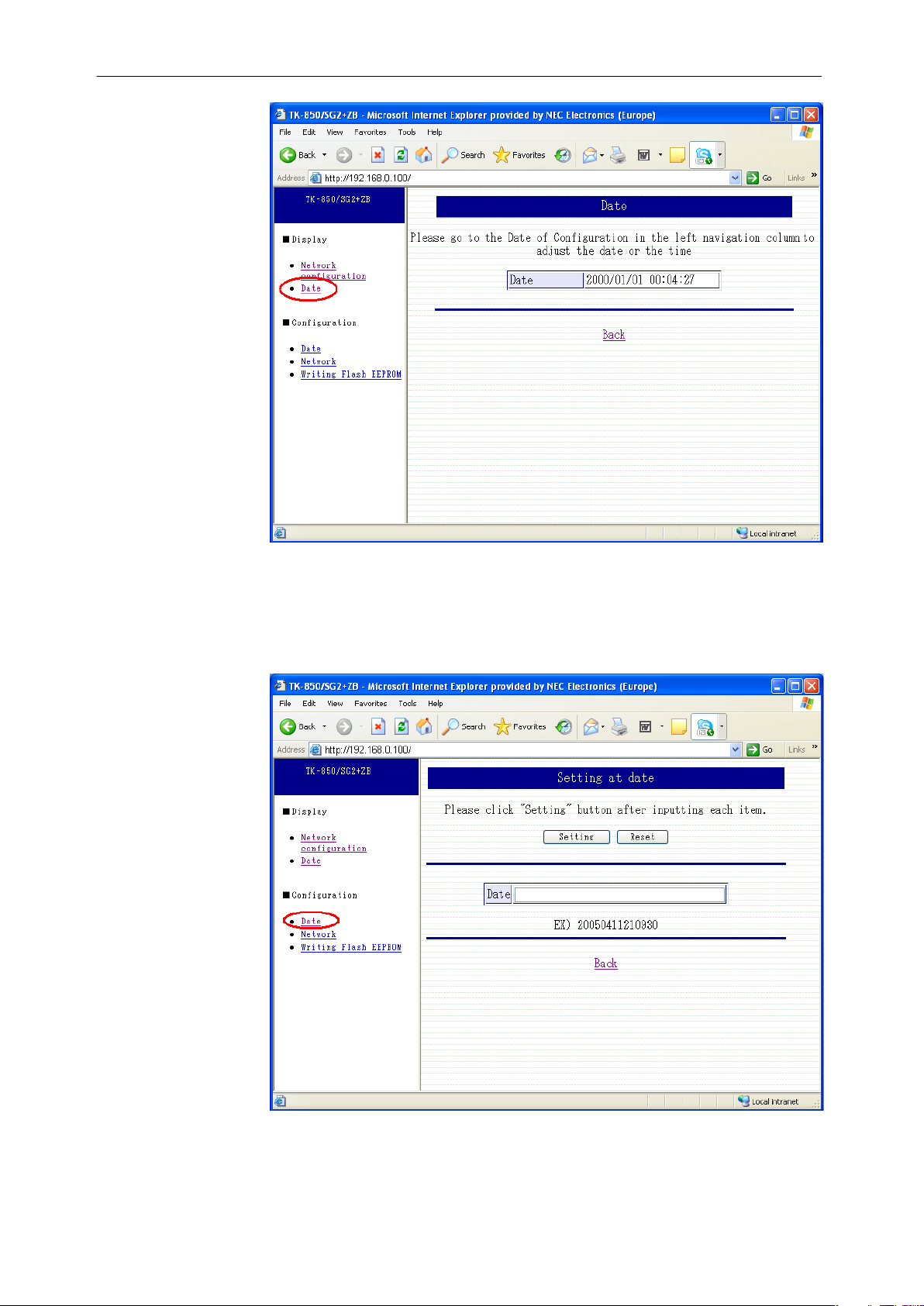
If you select [Display] -> [Date], you can find the time the sample program has.
(The default time is 2000/01/01 00:00:00)
User's Manual U19026EE3V0UM00
11
Page 12
Chapter 2 Sample Program
Figure 2-3 Date configuration screen
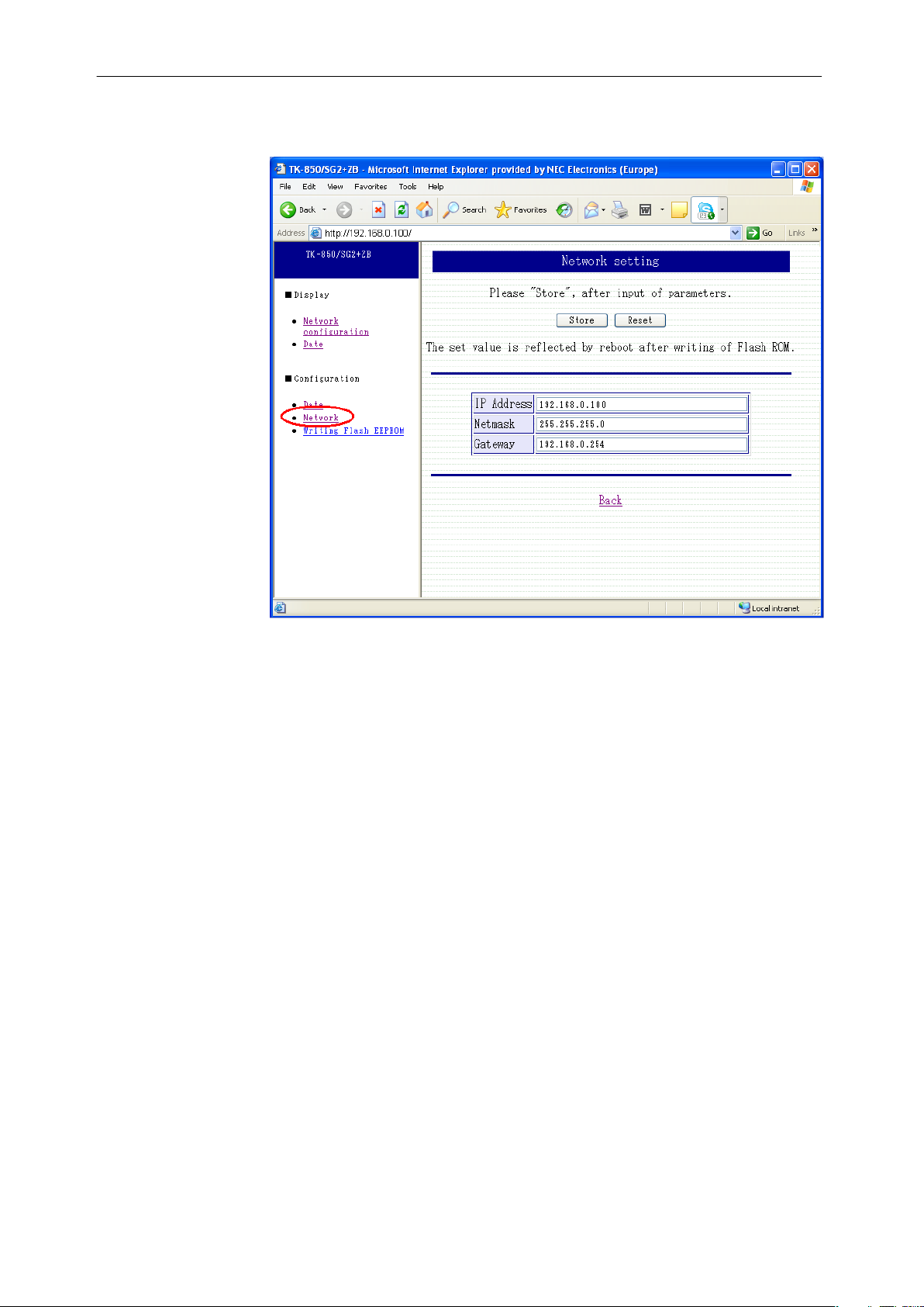
You can set the time by selecting [Configuration] -> [Date].
For example, if you want to set 9 minutes and 30 seconds past 9pm on April 11th
in 2005, please input 20050411210930.
12
Figure 2-4 Configuration of the date
To setup networks, select [Configuration] -> [Network].
User's Manual U19026EE3V0UM00
Page 13
Sample Program Chapter 2
You can modify the network configuration in this window. However it will be
adopted only after the new configuration is downloaded in the Flash EEPROM.
Figure 2-5 Configuration of the network parameters
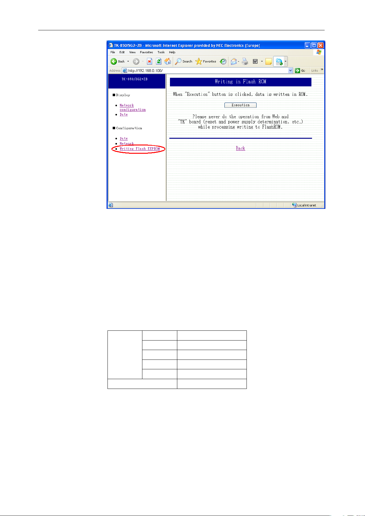
You can open the Flash programming window by selecting [Configuration] ->
[Writing Flash EEPROM].
Click the “Execution” button to store the current settings.
User's Manual U19026EE3V0UM00
13
Page 14
Chapter 2 Sample Program
Figure 2-6 Saving the new parameters by writing in the MCU Flash memory
2.2 Operation Procedure with TK-78K0/KF2+UZ boards
Once the TK-850/SG2+UZ board is ready (section "2.1 Operational procedure for
the TK-850/SG2+UZ" ), the connection of the TK-78K0/KF2+UZ remote node
(called Device) requires some settings.
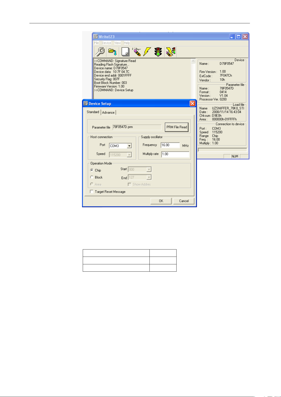
You can write the sample programs to the 78K0/KF2 built-in flash memory by
using the flash programming software WriteEZ3.
Set the switches of TK-78K0/KF2+UZ as shown in the following table:
Table 2-2 Flash programming mode settings for the TK-78K0/KF2+UZ
Bit 1 ON
Bit 2 ON
SW1
SW5 UART side
Bit 3 OFF
Bit 4 OFF
Bit 5 OFF
14
Using the Flash programmer WriteEZ3, load and write the file "mac78k0.hex"
which can be found under the following directory on the CDROM:
<CD>\SamplePrograms\SamplePrograms\Demo_78K0
or can be found in the directory where they have been installed by the automatic
process of the CDROM (see section "6.2.3 Sample Program Installation" ).
For further details, please refer to the documentation of the Flash programmer
WriteEZ3, or to the documentation provided with the TK-78K0/KF2+UZ board.
User's Manual U19026EE3V0UM00
Page 15
Sample Program Chapter 2
Figure 2-7 WriteEZ3 Device Setup
Write the same sample programs to the other TK-78K0/KF2+UZ boards.
Then, set the position of the switches as shown below:
Table 2-3 Operation mode setting for the TK-78K0/KF2+UZ
SW1 – 1, 2, 3, 4, 5, 6 and 7 OFF
SW1 - 8 ON
SW5 UART
When you run the application, you can run it as a stand-alone system by setting
JP1 to 2-3 pin short and using a 6LR61 9V battery connected to CN2. For further
details about the power supply settings, please refer to section "3. Hardware
specification" .
Apply the relevant power supply source to the target boards.
If you select [Display] -> [Network Configuration] and if a Device is connected
wirelessly, you can see the red line.
User's Manual U19026EE3V0UM00
15
Page 16
Chapter 2 Sample Program
Figure 2-8 Network configuration overview (with a Device connected)
Up to 4 devices can be connected in the sample program. To display the latest
status, click the "Update" button. The pink line indicates it is not connected.
The coordinator checks for a device every 30 seconds.
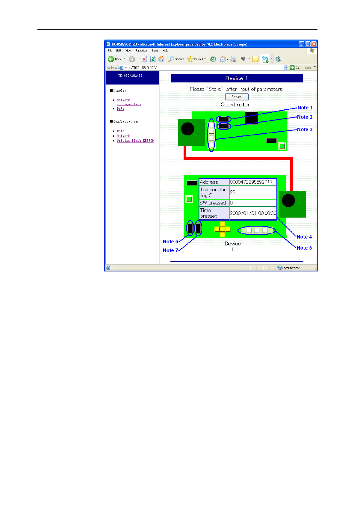
If you click a connected device (double click one of the device green box
connected with a red line), you can find the following window.
16
User's Manual U19026EE3V0UM00
Page 17
Sample Program Chapter 2
Figure 2-9 Details of a Device connection
The actions that can be performed via the WEB Browser interface are shown
below.
Notes
1. If you click the SW3 of the coordinator, LED3 on the physical Device 1 turns
on, and then, off .
2. If you click the SW2 of the coordinator, LED2 on the physical Device 1 turns
on, and then, off.
3. If you click any LEDs (LED1, LED2, LED3 or LED4), the corresponding LED
on the physical board will turn on, and off.
4. View of status information for the Device:
• Address: This is the MAC address of the Device in IEEE
802.15.4.
• Temperature: Measured on the Device
• SW pressed: Indicates which switch was pressed on the
Device.
• Time pressed: Time stamp of the pressed switch.
5. LEDs (LED2, LED3 or LED4) can be on and off.
6. If the SW3 of the Device is clicked, LED1 of the coordinator is on and off.
The information at the Note 4, SW pressed, and Time stamp, will be
updated.
7. If the SW4 of the Device is clicked, LED2 of the coordinator is on and off.
The information at the Note 4, SW pressed, and Time stamp, will be
updated.
User's Manual U19026EE3V0UM00
17
Page 18
Chapter 2 Sample Program
To update to the latest status, click the "Store" button.
Following are the different operations that can be directly done on the board:
• On the TK-850/SG2+UZ board:
- By pressing SW3 on the TK-850/SG2+UZ board, LED3 on the
Device 1 becomes on and off.
- By pressing SW2 on the TK-850/SG2+UZ board, LED2 on the
Device 1 becomes on and off
• On a TK-78K0/KF2+UZ board:
- By pressing SW3 on a TK-78K0/KF2+UZ board, LED1 of the
coordinator becomes on and off.
- By pressing SW4 on a TK-78K0/KF2+UZ board, LED2 of the
coordinator becomes on and off.
Please note LED’s manipulated on the board are not reflected on the Web
browser.
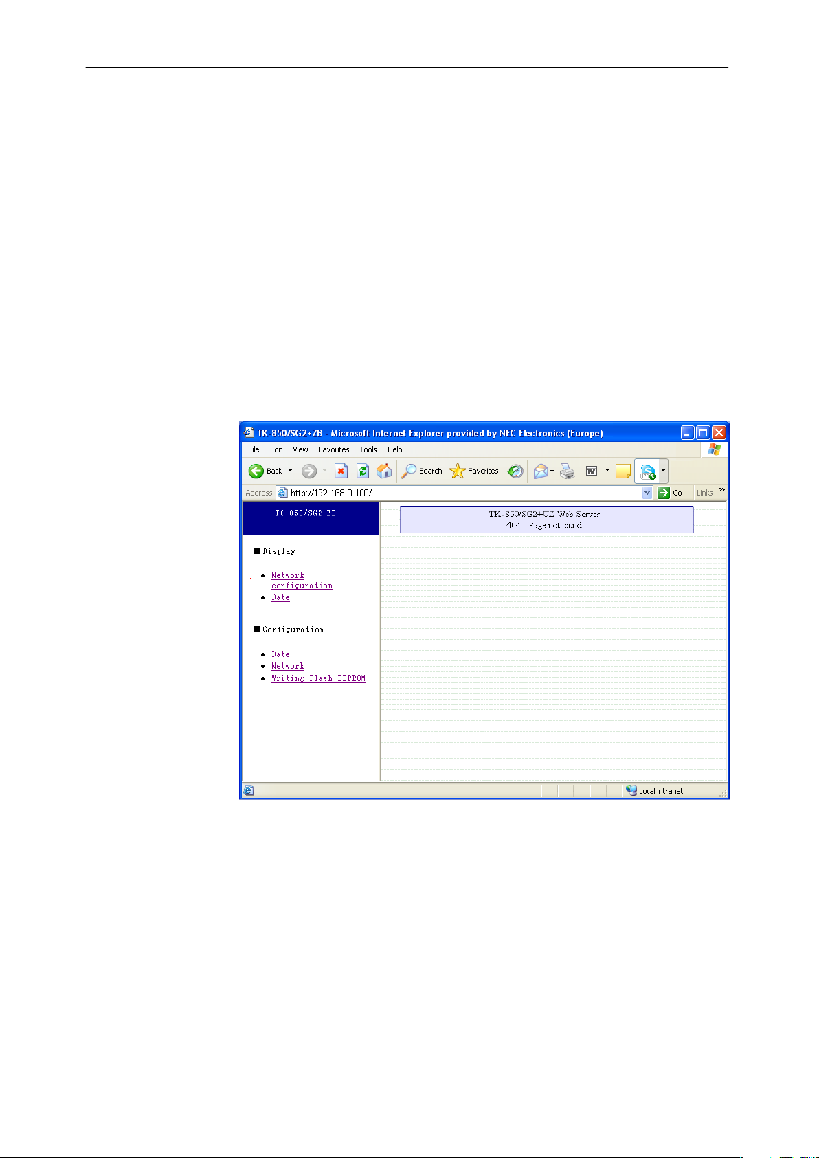
If you click a device, not connected with a red line, you will see the following
window.
18
Figure 2-10 Default screen for a non-connected device
User's Manual U19026EE3V0UM00
Page 19
Chapter 3 Hardware specification
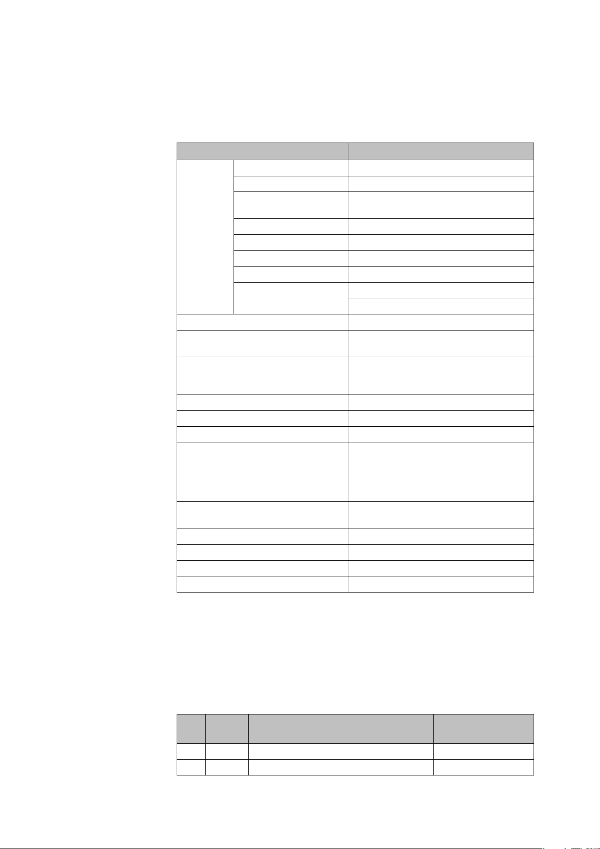
Table 3-1 General hardware features
Item Details
Part number μPD70F3281YGC-8EU
Operation with main clock 20 MHz
Clock
Internal flash memory 384 kB
CPU
USB interface Mini USB x 1 channel
Serial interface
Ethernet interface
CAN T/H pattern for external connection
RF board UZ2400 RF Board
Temperature sensor Temperature sensor x 1
LED
Multipurpose input
Reset Switch Push switch x 1
N-WIRE/MiniCube interface Not mounted
On board Flash memory writing Possible
Power supply 5.0V (USB supply) or 6.0V (battery supply)
Internal RAM 32 kB
Operation voltage 3.3 V
I/O voltage 3.3 V
Special mention
Main = 5 MHz
Subclock = 32.768 kHz
IIC included
CAN included
Equipped with Synchronous/Asynchronous
header pin
RJ-45 (10/100M) 1Port
MAC address setup = External EEPROM
State indication LED = 2
Red x 4 : LED 1 - 4 = Multipurpose
Green x 3 :
- LED 5 = Power
- LED 6 = LAN
- LED 7 = LINK
4-bit Slide switch x 1
Push switch x 2
3.1 Terminal list
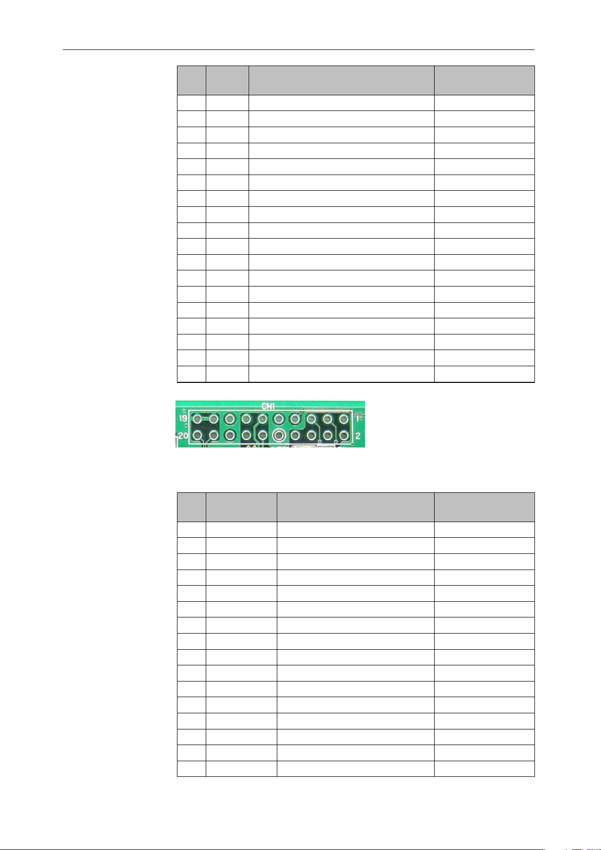
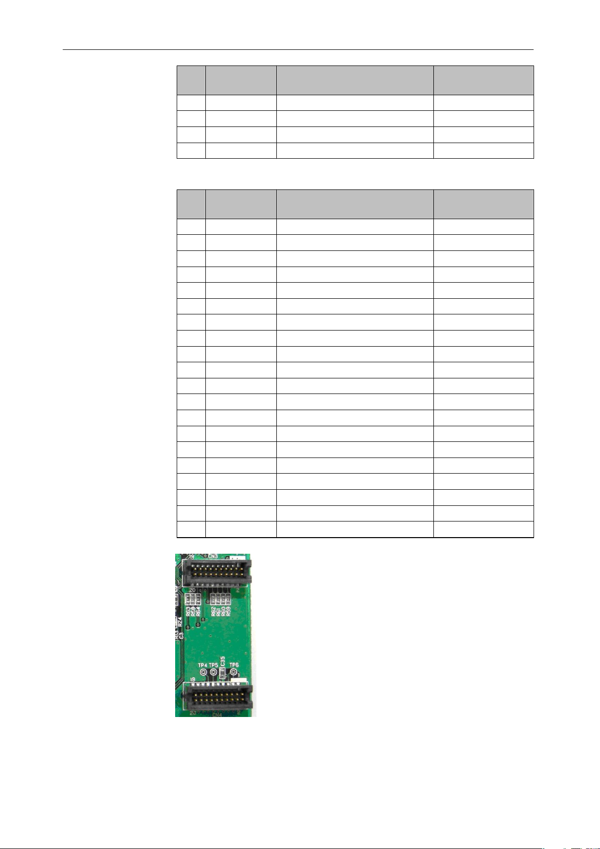
Terminal table of CN1, CN3 and CN4 of the CPU board.
Table 3-2 Connector CN1 terminal list
Signal
CN1
name
1 VDD VDD
2 P36 P36/CTXD0/IETX0
Terminal CPU name at connection
destination
User's Manual U19026EE3V0UM00
Notes
19
Page 20
Chapter 3 Hardware specification
Signal
CN1
name
3 P37 P37/CRXD0/IERX0
4 P38 P38/TXDA2/SDA00
5 P39 P39/RXDA2/SCL00
6 P53 P53/SIB2/KR3/TIQ00/TOQ00/RTP03/DDO Both use with N-Wire
7 P54 P54/SOB2/KR4/RTP04/DCK Both use with N-Wire
8 P55 P55/SCKB2/KR5/RTP05/DMS Both use with N-Wire
9 P70 P70/ANI0
10 P71 P71/ANI1
11 P72 P72/ANI2
12 P73 P73/ANI3
13 PCM1 PCM1/CLKOUT
14 PCM2 PCM2/HLDAK
15 PCM3 PCM3/HLDRQ
16 PCT1 PCT1/WR1
17 GND GND
18 PDH4 PDH4/A20
19 GND GND
20 PDH5 PDH5/A21
Terminal CPU name at connection
destination
Notes
Figure 3-1 Connector CN1 pin configuration
Table 3-3 Connector CN3 terminal list
CN3 Signal name
1 GND GND
2 N.C.
3 VREG_EN P02/NMI Output from CPU
4 N.C.
5 RESn P03/INTP0/ADTRG Output from CPU
6 FIFO P10/ANO0 Input to CPU
7 N.C.
8 FIFOP P06/INTP3 Input to CPU
9 N.C.
10 CCA P11/ANO1 Input to CPU
11 N.C.
12 SFD P33/TIP01/TOP01 Input to CPU
13 N.C.
14 CSn P34/TIP10/TOP10 Output from CPU
15 N.C.
16 SCLK P42/SCKB0 Output from CPU
Terminal CPU name at
connection destination
Notes
20
User's Manual U19026EE3V0UM00
Page 21
Hardware specification Chapter 3
CN3 Signal name
17 N.C.
18 SI P41/SOB0 Output from CPU
19 GND GND
20 SO P40/SIB0 Input to CPU
Terminal CPU name at
connection destination
Table 3-4 Connector CN4 terminal list
CN4 Signal name
1 TP6
2 GND GND
3 TP6
4 GND GND
5 TP6
6 GND GND
7 3.3V
8 GND GND
9 3.3V
10 GND GND
11 TP5
12 GND GND
13 TP4
14 GND GND
15 N.C.
16 GND GND
17 N.C.
18 GND GND
19 N.C.
20 GND GND
Terminal CPU name at
connection destination
Notes
Notes
Figure 3-2 Connector CN3 (top) and CN4 (bottom) pin configuration
User's Manual U19026EE3V0UM00
21
Page 22
Chapter 3 Hardware specification
3.2 Switches and LED
3.2.1 SW1, JP1
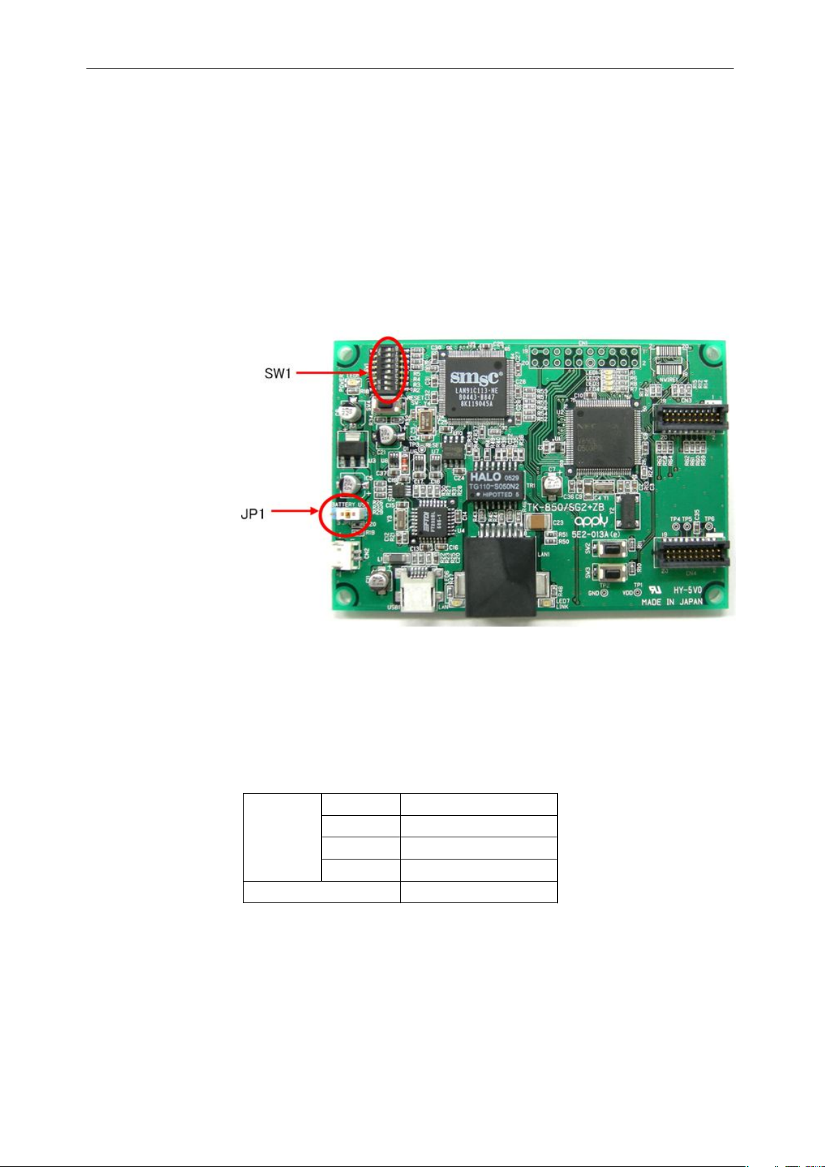
Bit1, 2, 3 and 4 of SW1 are dip switches for Operation Mode setting.
Bit5, 6, 7 and 8 of SW1 are connected to P74, P75, P76 and P77 for multipurpose
input.
JP1 is a jumper to select a power source.
Figure 3-3 SW1 and JP1
3.2.1.1
Table 3-5 Flash programming mode settings for the TK-850/SG2+UZ
3.2.1.2
Flash Programming Mode with WriteEZ1
The Flash memory of the V850ES/SG2 microcontroller (integrated in the TK-850/
SG2+UZ board) can be programmed using the attached software WriteEZ1 in
your PC, if the following switch and jumper settings are made.
Bit 1 ON
SW1
JP1 USB side (1-2-pin short)
Bit 2 OFF
Bit 3 ON
Bit 4 ON
On-chip debug Mode with the IAR TK-interface
The following setting activates the On-chip debug functions for the TK-850/SG2
+UZ board.
22
User's Manual U19026EE3V0UM00
Page 23
Hardware specification Chapter 3
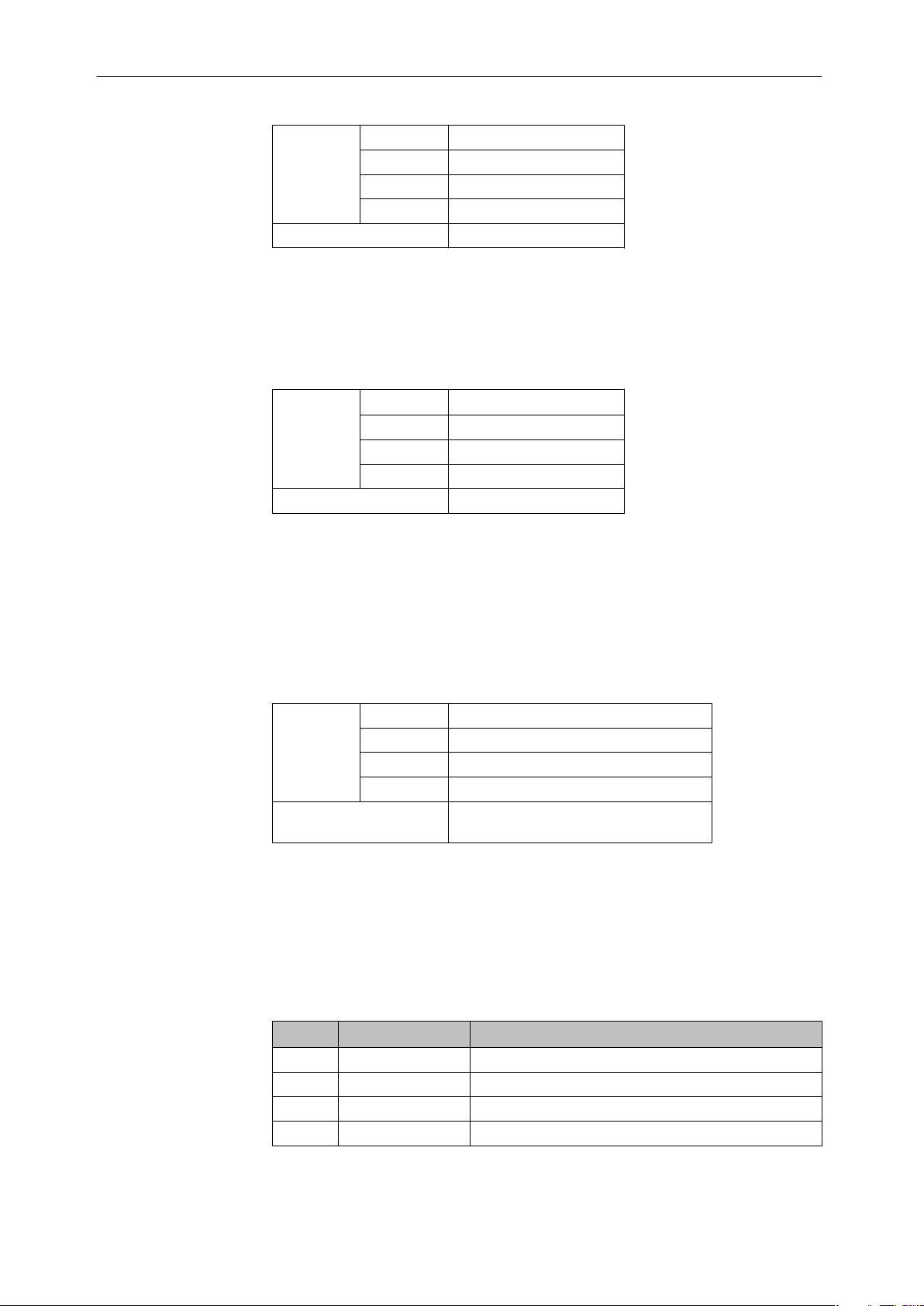
Table 3-6 On-chip debug mode settings for the TK-850/SG2+UZ
Bit 1 ON
SW1
JP1 USB side (1-2-pin short)
Bit 2 ON
Bit 3 ON
Bit 4 OFF
3.2.1.3
N-Wire Connecting Mode
Change to the following settings when you connect to N-Wire emulator to the
TK-850/SG2+UZ board.
Table 3-7 N-wire connecting mode settings for the TK-850/SG2-UZ
Bit 1
SW1
JP1 USB side (1-2-pin short)
Bit 2 OFF
Bit 3 OFF
Bit 4 OFF
ON or OFF
Note
Note: Please set ON, if you make COM communication to host machine using the
P30/TXDA0,P31/RXDA0 pin.
3.2.1.4
Normal Operation Mode
Change to the following settings when you execute the program normally. Select
the power source chosen with the JP1.
Table 3-8 Normal operation mode settings for the TK-850/SG2+UZ
Bit 1 OFF
SW1
JP1
Bit 2 OFF
Bit 3 OFF
Bit 4 OFF
USB powered (1-2-pin short)
Battery powered with CN2 (2-3-pin short)
3.2.1.5
General purpose setting port
Bit 5, 6, 7 and 8 of SW1 are general purpose setting ports.
The port state is “Low” because it is connected to GND when the switch is ON.
The port state is “High” because it is connected to a 10kΩ pull-up resistor, when
the switch is OFF.
Table 3-9 Switch SW1 terminal list
SW1 Signal name Terminal CPU name at connection destination
Bit 5 P74 P74/ANI4
Bit 6 P75 P75/ANI5
Bit 7 P76 P76/ANI6
Bit 8 P77 P77/ANI7
User's Manual U19026EE3V0UM00
23
Page 24
Chapter 3 Hardware specification
3.2.2 SW2, SW3
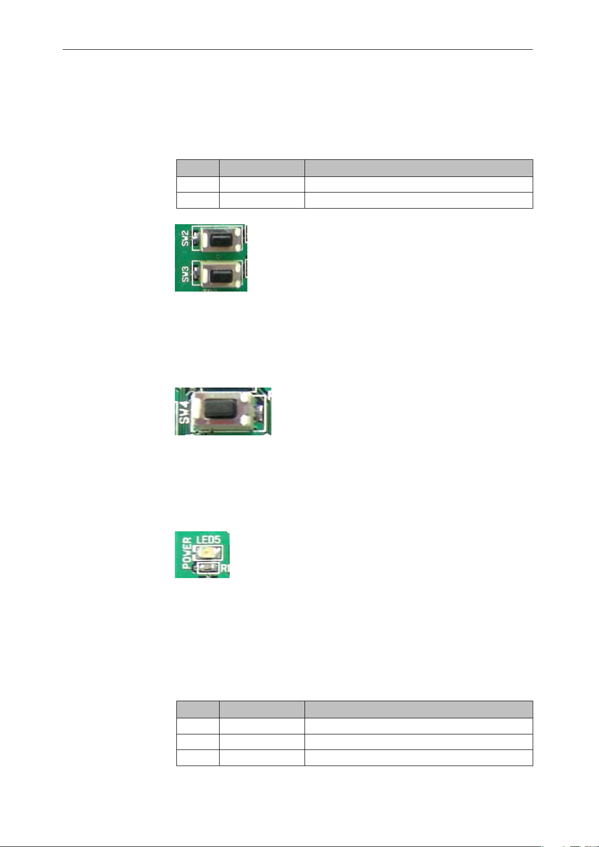
SW2 and SW3 are push switches. They are connected to pull-up resistors, and
their outputs go “Low”, when they are pushed.
Table 3-10 Switch SW2 and SW3 terminal list
Switch Signal name Terminal CPU name at connection destination
SW2 P50 P50/TIQ01/TOQ01/RTP00/KR0
SW3 P51 P51/TIQ02/TOQ02/RTP01/KR1
Figure 3-4 Switches SW2 and SW3
3.2.3 SW4
SW4 is the reset switch. The TK-850/SG2+UZ board is reset when SW4 is pushed.
Figure 3-5 Switch SW4
3.2.4 LED5
The `Power LED’ LED5 is activated when the power supply is turned on.
Figure 3-6 LED5 as Power LED
3.2.5 LED1, LED2, LED3 and LED4
24
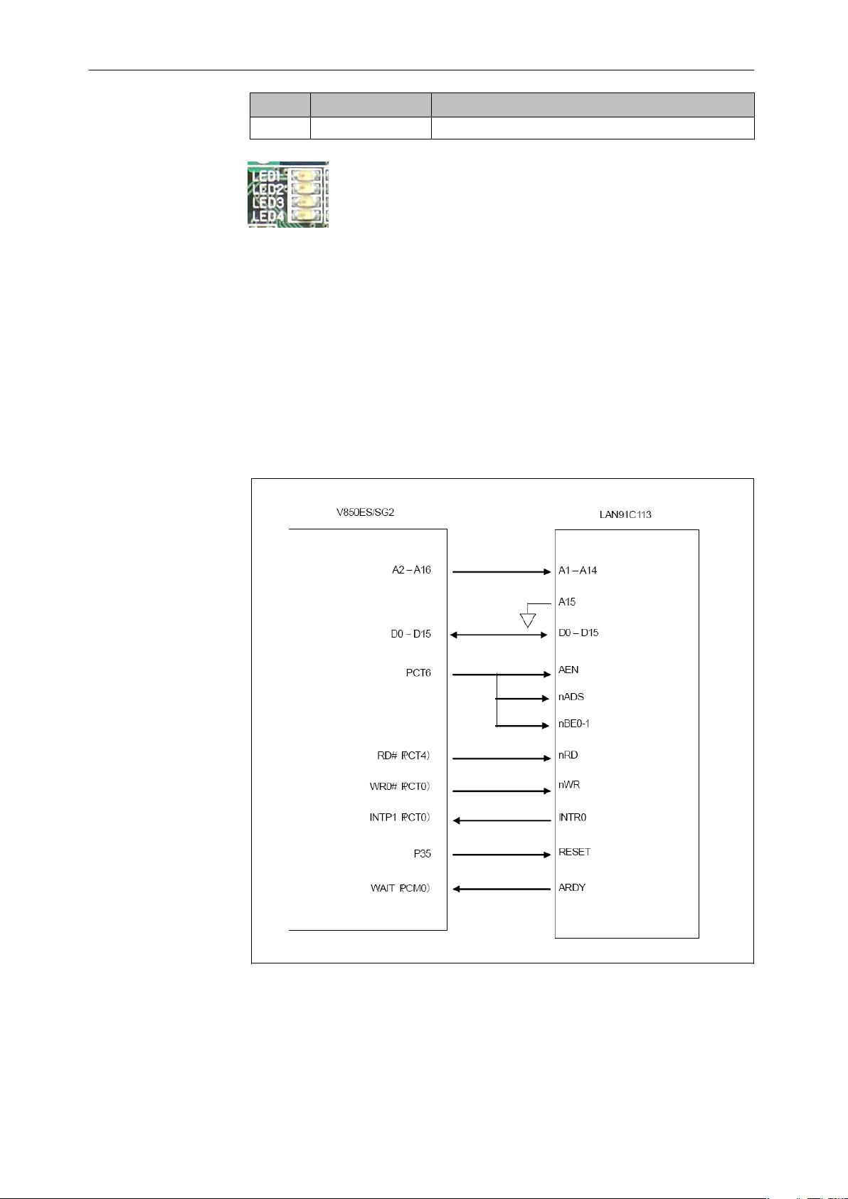
LED1, 2, 3 and 4 are available for applications. To turn on a LED, set the output
port to “Low”.
Table 3-11 LED 1, 2, 3 and 4 terminal list
LED Signal name Terminal CPU name at connection destination
LED1 PDH0 PDH0
LED2 PDH1 PDH1
LED3 PDH3 PDH3
User's Manual U19026EE3V0UM00
Page 25
Hardware specification Chapter 3
LED Signal name Terminal CPU name at connection destination
LED4 PDH2 PDH2
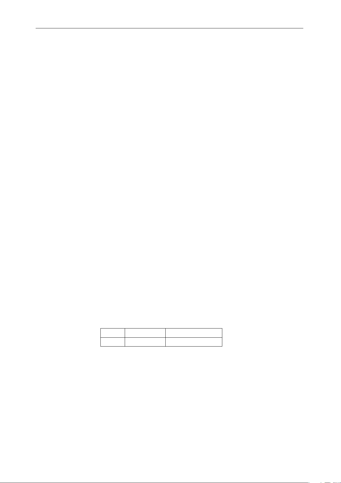
Figure 3-7 LED 1, 2, 3 and 4
3.3 LAN Controller
The TK-850/SG2-UZ board has a LAN controller, LAN91C113 made by SMSC.
3.3.1 Connection
Connection of CPU to LAN controller is below.
Figure 3-8 V850ES/SG2 and LAN controller pin connection
User's Manual U19026EE3V0UM00
25
Page 26
Chapter 3 Hardware specification
3.3.2 Reset of LAN Controller
P35 is used to reset the LAN controller. When P35 is Hi-z after CPU reset, the
LAN controller will be in reset state. Before releasing the reset, please change the
CPU port “Chip Select Signal (AEN,nADS)” and “Read/Write Signal” to be inactive
level. And then drive the P35 to “Low”. And release the reset.
The Ethernet MAC address is initialized by the contents of the serial EEPROM,
after release of the reset.
3.3.3 Access to the LAN Controller
It is necessary to set the microcontroller to external bus mode to access the LAN
controller. The external LAN controller is configured to operate in 16-bit (word)
mode, and therefore, the external bus will need to be set-up for "word wide" read
and write access modes.
3.4 Temperature Sensor
The TK-850/SG2+UZ board has a temperature sensor for measuring the ambient
temperature of the PWB board. It is connected to the analogue input pin P79/
ANI9 of the microcontroller.
• Temperature sensor S-8120C (Made by SII)
• Power supply of sensor : +3.3V
• Linear output voltage : -8.20mV/°C ( from -20°C to 80°C )
Please refer to the datasheet for details.
3.5 Power Supply
There are two choices to supply power to the board, USB or a 6LR614 9V battery
via CN2. Please refer to the following table for the jumper setting.
Table 3-12 JP1 Setting for the power supply source
JP1 USB Power USB (1-2-pin short)
Battery CN2 (2-3-pin short)
26
Please replace the battery with a new one, if the voltage level goes down to 4.75V.
Below the voltage level of 4.75V, functions of the board are not guaranteed.
The battery voltage can be checked at the port as shown below.
User's Manual U19026EE3V0UM00
Page 27

Hardware specification Chapter 3
Table 3-13 9V Battery checking
Signal
name
BT_MONI P78/ANI8
Terminal CPU name at
connection destination
Notes
About 0.265 times of input power supply
For instance
If the battery level 6.0V:
The level of the BT_MONI = 0.265x6.0
= 1.59(V)
If the battery level is 4.75V:
The level of the BT_MONI = 0.265x4.75
= 1.25(V)
User's Manual U19026EE3V0UM00
27
Page 28
Chapter 4 TK-850/SG2+UZ Data
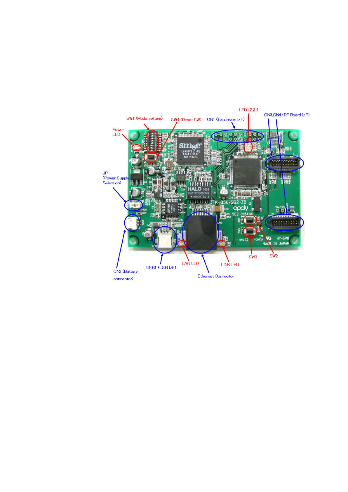
4.1 Parts Layout
Figure 4-1 Hardware overview of theTK-850/SG2+UZ board
28
User's Manual U19026EE3V0UM00
Page 29
TK-850/SG2+UZ Data Chapter 4
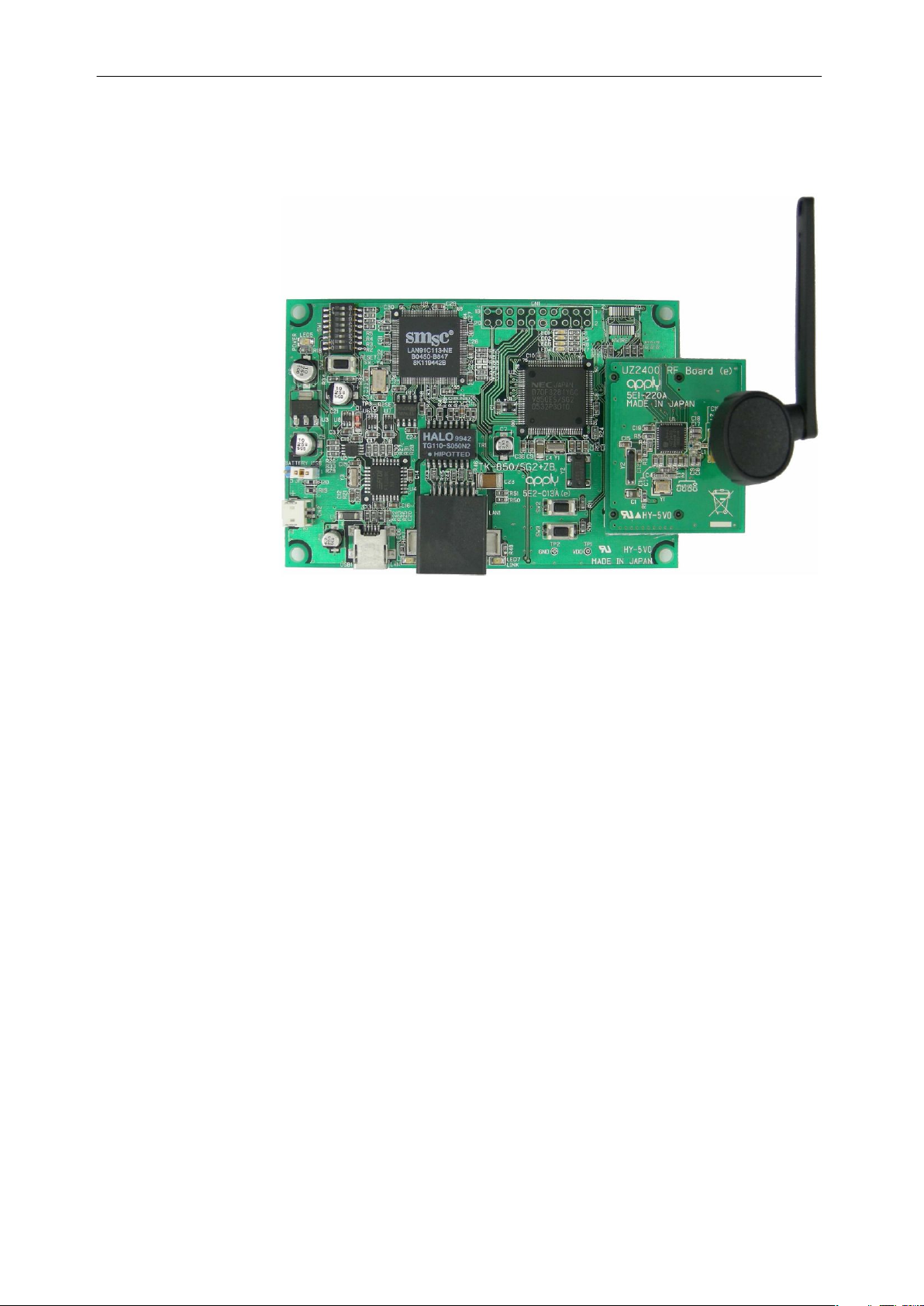
4.2 RF Board connection figure
Figure 4-2 Overview of the connection of the RF board
User's Manual U19026EE3V0UM00
29
Page 30
Chapter 5 Programming the TK-850/SG2+UZ with
WriteEZ1
WriteEZ1is the flash memory programming software which can erase and
program directly the flash memory of the microcontroller of the board via the USB
interface.
For details about the installation of the Flash Programmer WriteEZ1 software or
about the driver required for use, please refer to the section "6. V850 ZigBee
Gateway Development Platform, Installation and Operation"
To use WriteEZ1, please set the mode switch on the TK-850/SG2+UZ board as
follows. Then, please connect the board to your PC with a USB cable.
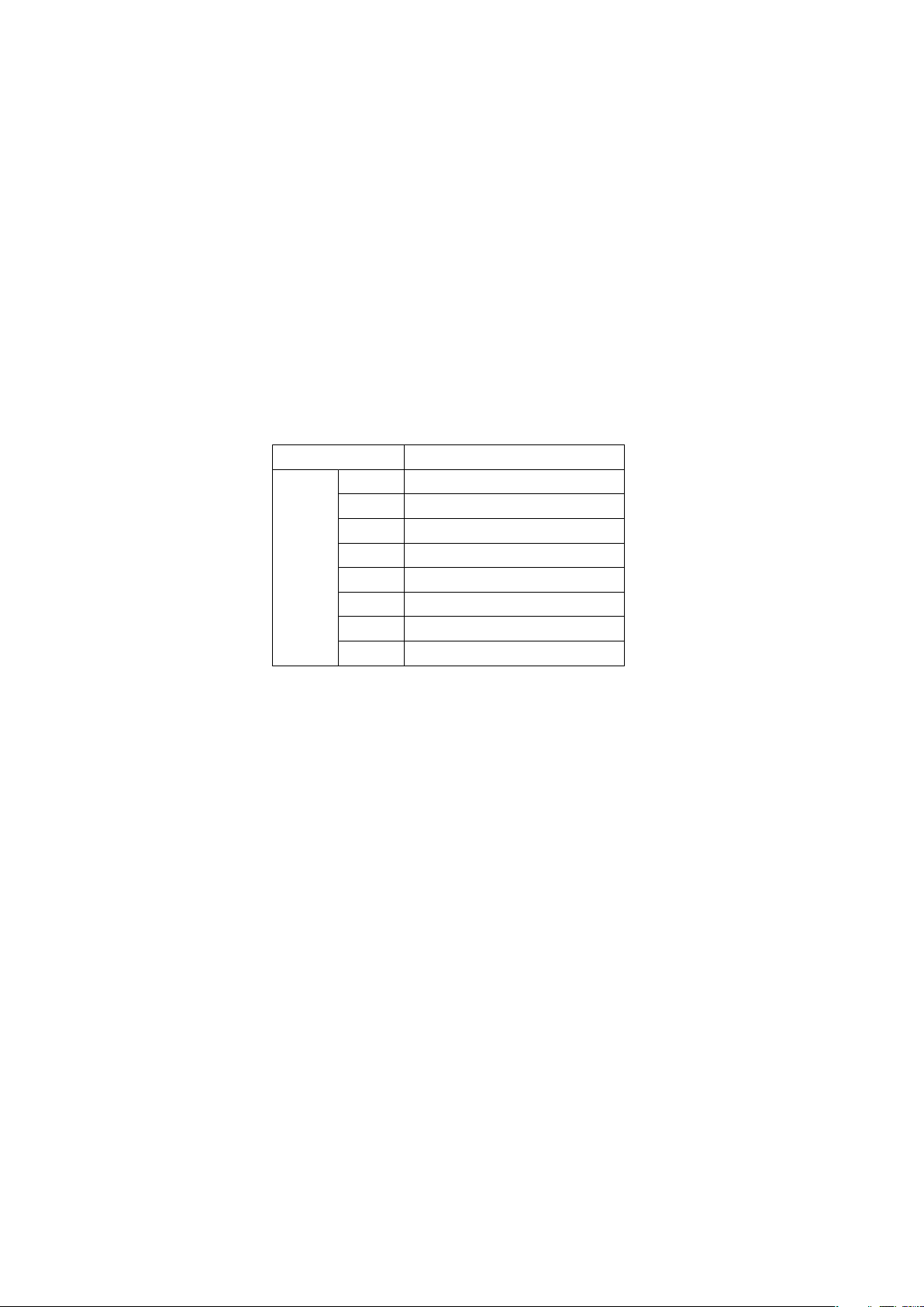
Table 5-1 Flash programming mode settings for the TK-850/SG2+UZ
JP1 1-2-pin short (USB side)
Bit 1 ON
Bit 2 OFF
Bit 3 ON
SW1
Bit 4 ON
Bit 5 OFF
Bit 6 OFF
Bit 7 OFF
Bit 8 OFF
Please start WriteEZ1 by selecting [Programs] -> [NEC Electronics Tools] ->
[WriteEZ1] in your Windows [Start] menu.
30
User's Manual U19026EE3V0UM00
Page 31
Programming the TK-850/SG2+UZ with WriteEZ1 Chapter 5
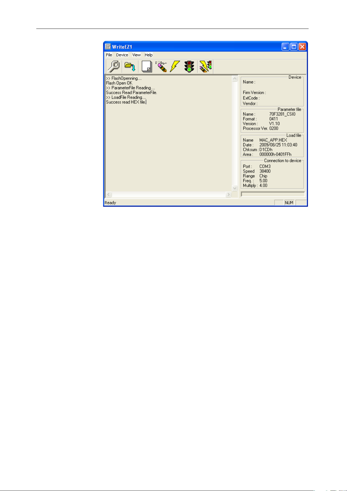
Figure 5-1 GUI interface of the Flash programmer WriteEZ1
Please select the “Setup” button in the menu bar or [Device] -> [Setup].
Then select the”PRM File Read” button.
User's Manual U19026EE3V0UM00
31
Page 32
Chapter 5 Programming the TK-850/SG2+UZ with WriteEZ1
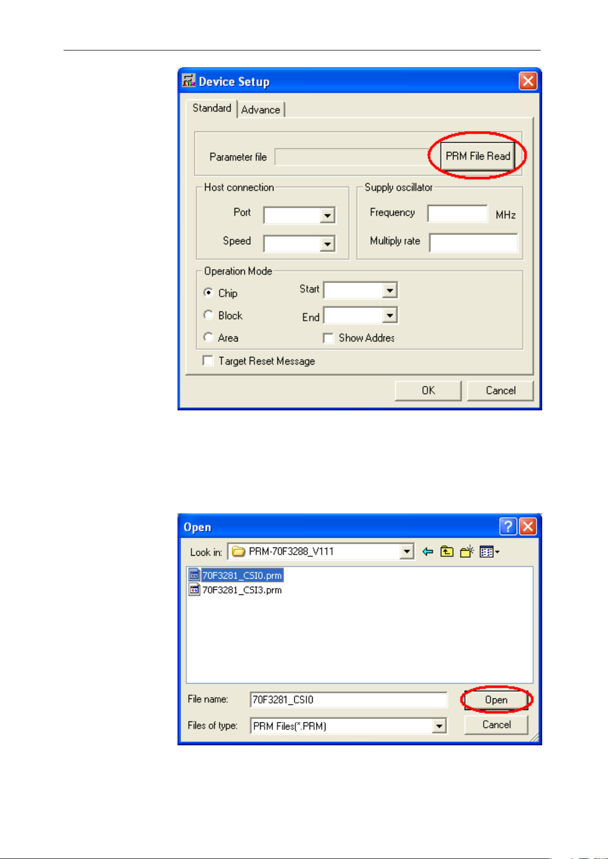
Figure 5-2 Device setup screen
The PRM file contains the device-specific parameter required for programming.
You will also find the PRM files in the CDROM in the following directory:
<CD>\NEC Tools 32\PRM-70F3288_V111
Please select the following PRM file:
<CD>\NEC Tools 32\PRM-70F3288_V111\70F3281_CSI0.prm
32
Figure 5-3 Choice of the parameter file PRM for the V850ES/SG2 microcontroller
User's Manual U19026EE3V0UM00
Page 33
Programming the TK-850/SG2+UZ with WriteEZ1 Chapter 5
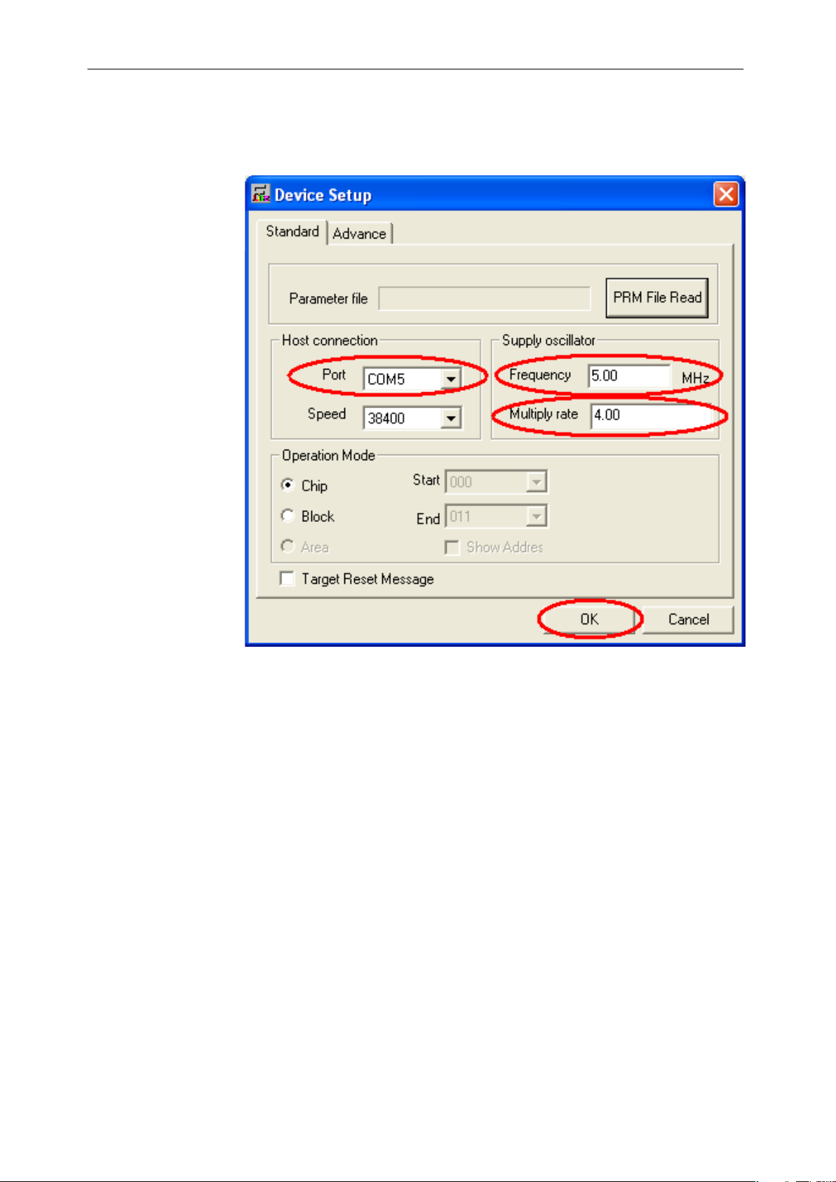
Select the COM port number you connected your PC with the TK board. All of
COM port numbers available on your PC will be displayed.
Set ”Speed” to 38400, ”Frequency” to 5.00, “Multiply rate” to 4.00.
Then, press “OK”.
Figure 5-4 Setting the parameters for the flash programming session
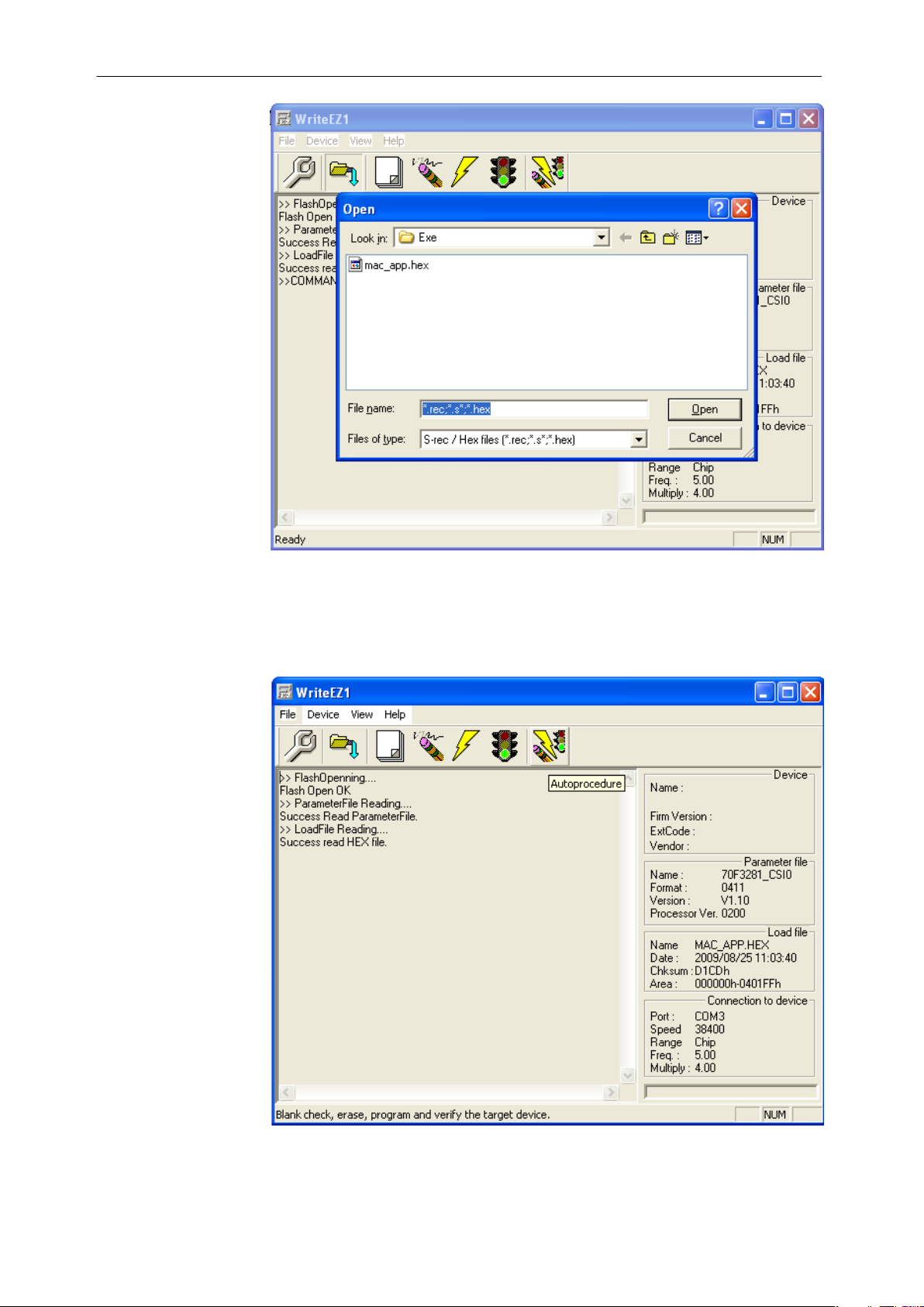
Next, load the HEX file that you want to program to WriteEZ1. Click “Load” to
open the file “mac_app.hex”, which you created in the section "7.4 Generating a
Hex file for flash programming" .
When successfully loaded, “Success read HEX file.” is displayed.
User's Manual U19026EE3V0UM00
33
Page 34
Chapter 5 Programming the TK-850/SG2+UZ with WriteEZ1
Figure 5-5 Loading the executable file .HEX
Next, write the programs by clicking “Auto procedure”.
When “Auto procedure” is clicked, it processes the “Erase” and “Program”
commands.
34
Figure 5-6 Starting the «Auto Procedure» to erase and program the Flash memory
User's Manual U19026EE3V0UM00
Page 35

Programming the TK-850/SG2+UZ with WriteEZ1 Chapter 5
When “Flash internal Verify OK!”, is displayed it means the flash memory writing
has successfully completed.
The programs are successfully written to the Flash memory of the V850/SG2
integrated in the board TK-850/SG2+UZ.
Disconnect the USB cable from TK-850/SG2+UZ board.
User's Manual U19026EE3V0UM00
35
Page 36

Chapter 6 V850 ZigBee Gateway Development
Platform, Installation and Operation
The IAR Embedded Workbench including the C-SPY debugger allows the user to
build and download application programs to the V850 ZigBeeTM Gateway
Development Platform. As the communication interface between the PC host
system and the V850 ZigBeeTM Gateway Development Platform board is USB, a
USB interface line is needed. Before you can download and run a program,
relevant software and hardware must be installed properly.
CDROM contents:
• IAR Embedded Workbench for V850 Kickstart version
• GUI Software for flash programming
• IEEE 802.15.4 MAC library
• Sample Programs
• Documentation
6.1 Hardware Installation
After unpacking V850 ZigBeeTM Gateway Development Platform, connect the
board to your host computer using the provided USB interface cable. When V850
ZigBeeTM Gateway Development Platform is connected, the USB driver needs to
be installed on the host machine. Please refer to the specific section "6.3 USB
Driver Installation" .
6.2 Software Installation
The V850 ZigBeeTM Gateway Development Platform package comes with the
following software demo packages:
• IAR Systems Embedded Workbench for V850 including C compiler,
assembler, linker, librarian and IAR C-SPYdebugger / simulator
• GUI software for flash programming
• Sample programs
6.2.1 IAR Systems Embedded Workbench installation
The IAR Systems Embedded Workbench must be installed on your PC. For
detailed installation hints, refer to the corresponding documentation of the IAR
Embedded Workbench: “IAR Systems Embedded Workbench for V850
installation”.
36
To install the IAR Systems Embedded Workbench for V850 including C-SPY
debugger / simulator, select the AUTORUN program in the directory <CD>\IAR
of the CDROM. The setup dialogues will guide you through the installation
process.
User's Manual U19026EE3V0UM00
Page 37

V850 ZigBee Gateway Development Platform, Installation
and Operation
6.2.2 GUI software WriteEZ1 for Flash Programming
The GUI software WriteEZ1 for flash programming is required to program the
Nodes with the Sample Programs. To install the WriteEZ1, select the “setup.exe”
program that can be found in the following directory in the CDROM provided:
<CD>\NEC Tools 32\WriteEZ1. The setup dialogues will guide you through the
installation process.
You will also need to install the USB driver required to emulate the UART
communication (which is the only one supported for the flash programming
interface) by the USB communication. Details about the installation procedure can
be found in the section "6.3 USB Driver Installation" .
6.2.3 Sample Program Installation
To install the sample/demonstration program for the V850 ZigBeeTM Gateway
Development Platform board, select the SETUP program in the directory <CD>
\SamplePrograms\ of the CDROM. The setup dialogue will guide you through the
installation process.
Chapter 6
6.3 USB Driver Installation
In order to use the V850 ZigBeeTM Gateway Development Platform board for OnChip debugging or FLASH programming, the USB driver needs to be installed on
the host machine. Two different drivers need to be installed:
- the USB serial converter
- the USB serial port
Install the drivers according to the following procedure:
• Installation on Windows 2000
• Installation on Windows XP
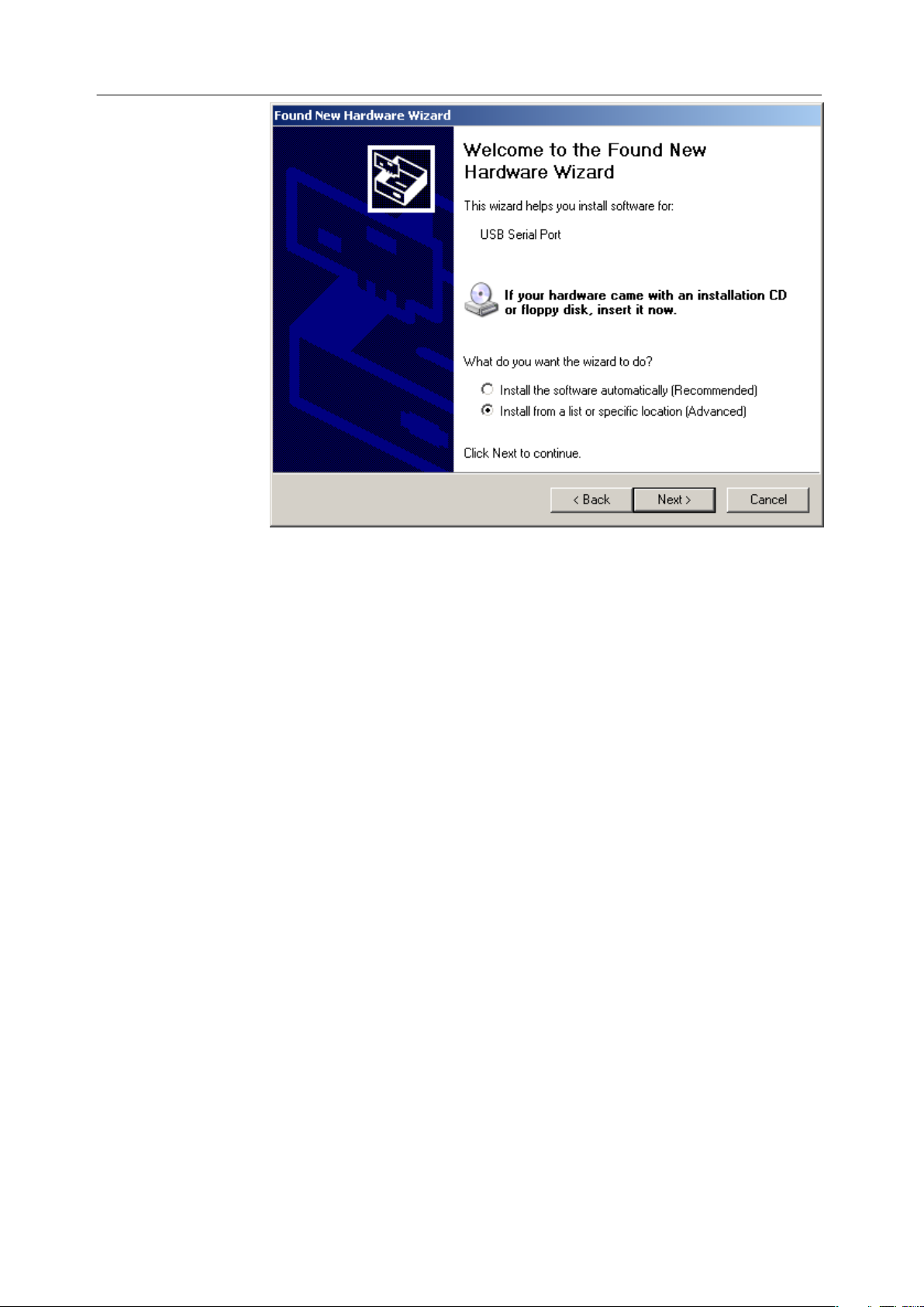
6.3.1 Installation on Windows XP
When the V850 ZigBee™ PRO Gateway Development Platform board is
connected with the host machine, the board is recognized by Plug and Play, and
the wizard for finding new hardware is started. Check that "Install from a list or
specific ..." is selected, then click Next >.
User's Manual U19026EE3V0UM00
37
Page 38
Chapter 6 V850 ZigBee Gateway Development Platform, Installation
and Operation
Figure 6-1 Found New Hardware Wizard 2 (Windows XP)
Check "Include this location in the search:" check box and browse to the
NEC Tools 32\drivers_virtual_uart\FTDI folder.
Click “Continue Anyway” when prompted to the Windows XP certification
compatibility.
Confirmation of USB Driver Installation
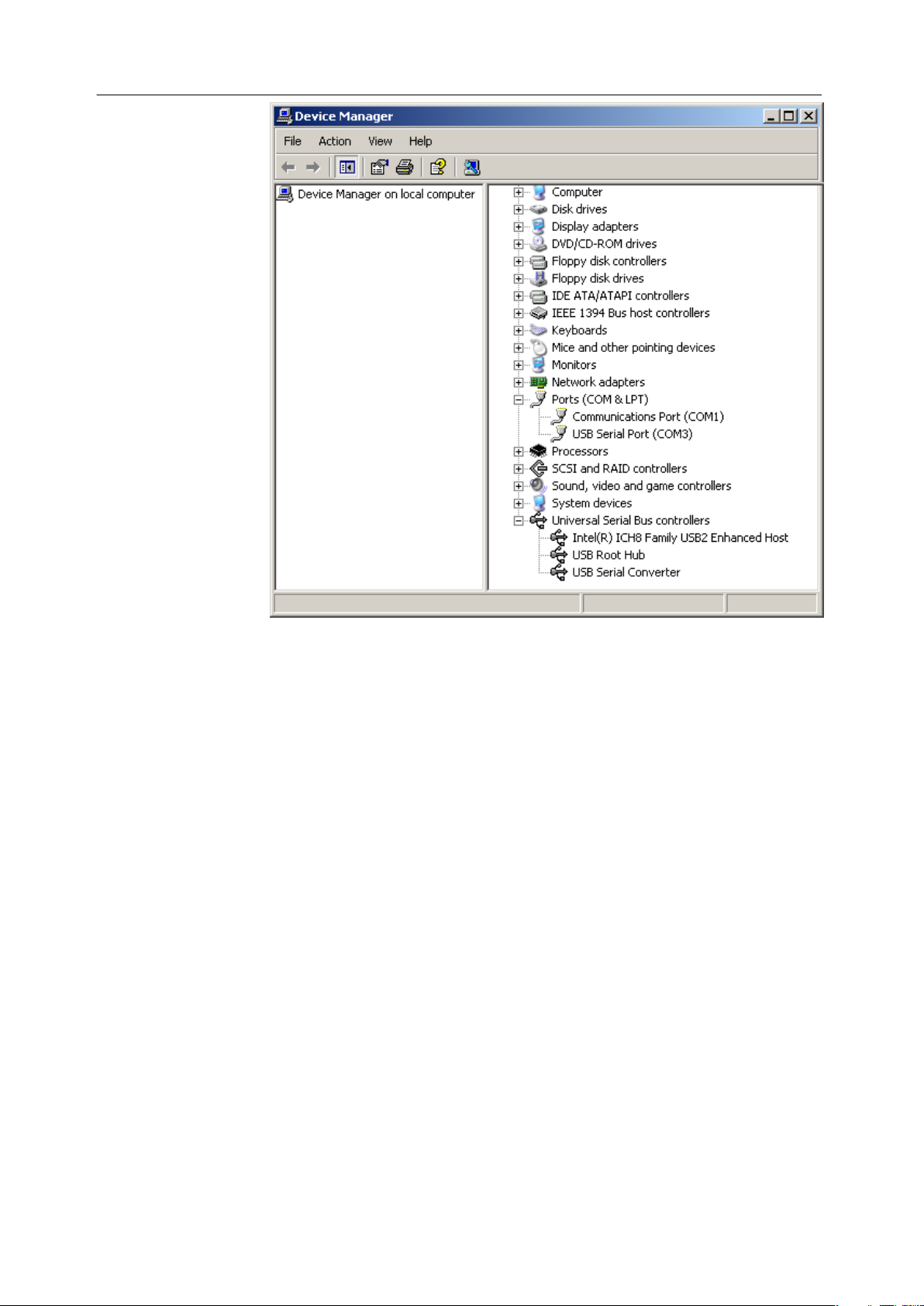
After installing the two types of drivers, check that the drivers have been installed
normally, according to the procedure below. When using the board in combination
with WriteEZ GUI, the information to be checked here is needed.
By clicking the "Device Manager" tab, check that the drivers are installed normally.
38
User's Manual U19026EE3V0UM00
Page 39
V850 ZigBee Gateway Development Platform, Installation
and Operation
Chapter 6
Figure 6-2 Device Manager
For Windows 2000/XP
Caution
Do not perform "Hardware Modification Scan" when communicating with the
target device.
Remark
In the flash programming WriteEZ GUI port list box, the same communication port
as COMxx of the USB Serial Port (in this case COM3 as shown in above
screenshot) needs to be selected.
User's Manual U19026EE3V0UM00
39
Page 40
Chapter 7 IAR Sample Session
7.1 Sample Structure
The V850 ZigBeeTM Gateway sample projects for IAR Systems Embedded
Workbench can be found directly in the CDROM in the folder:
<CD>\SamplePrograms\SamplePrograms, or can be found in the directory where
they have been installed by the automatic process of the CDROM (see section
"6.2.3 Sample Program Installation" ).
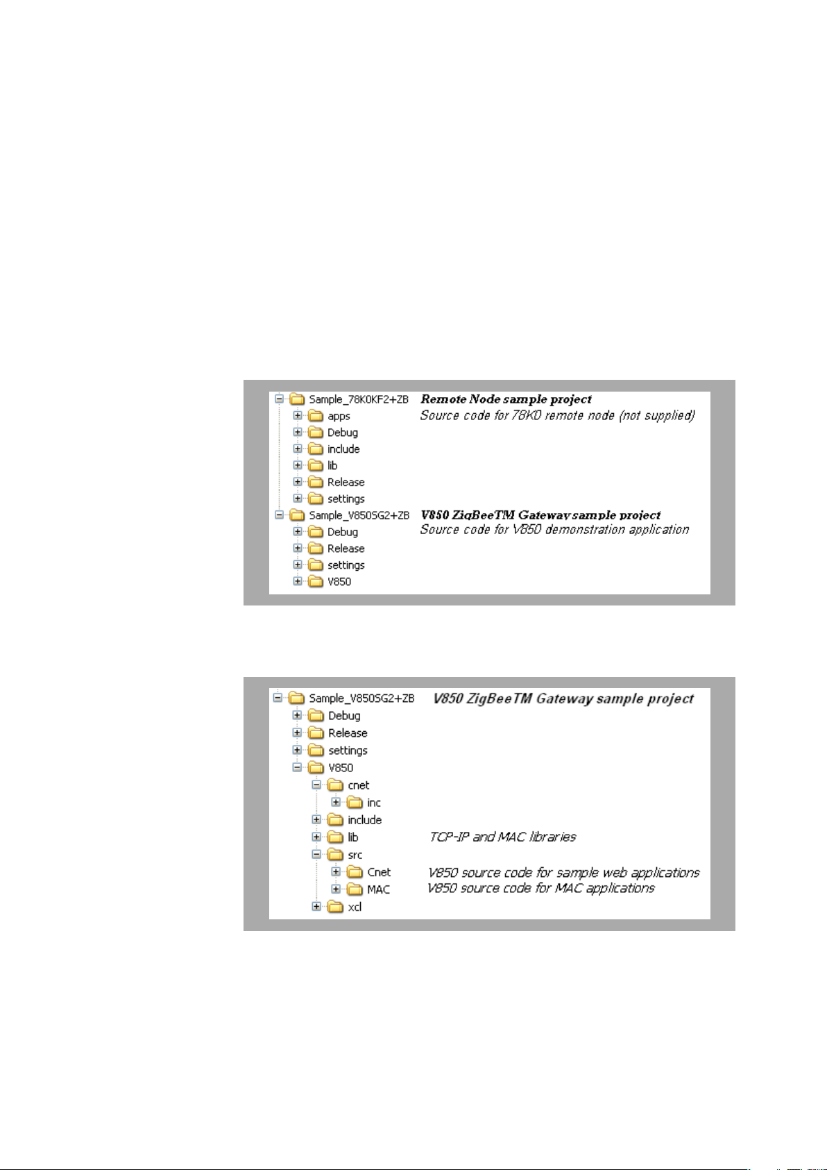
The sample projects are using the following folder structure:
Figure 7-1 Sample Programs project structure
Below is the detailed structure of the V850 ZigBeeTM Gateway Sample Project
Figure 7-2 Sample project structure
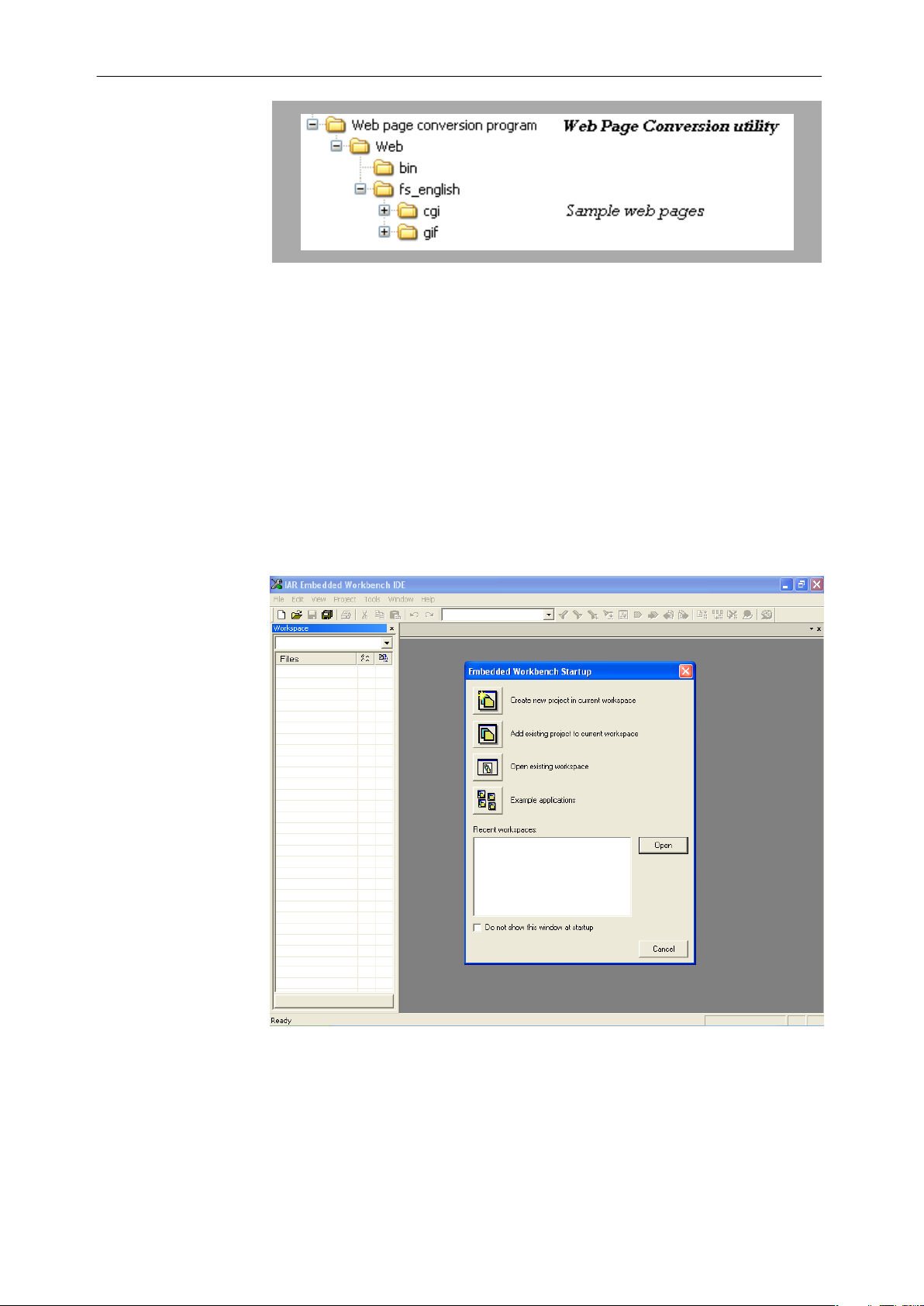
Below is the detailed structure of the Web page file that can be found in the
directory <CD>\Web page conversion program.
40
User's Manual U19026EE3V0UM00
Page 41
IAR Sample Session Chapter 7
Figure 7-3 Web page file structure
To create your own application using the MAC & TCPIP-stack, please make a
copy of the sample and use it as a template. All output files generated by the
development tools are located in a subfolder using the name of the corresponding
target. You can delete this folder before copying the sample application.
7.2 Project Loading
When everything is set up correctly the IAR Embedded Workbench can be started.
To do so, start the Embedded Workbench from Windows [Start] menu ->
[Programs] -> folder [IAR Systems] -> [IAR Embedded Workbench Kickstart for
V850]. The following screen appears:
Figure 7-4 IAR Embedded Workbench startup screen
Now select the option [Open exiting workspace] from the [File] menu and locate
the V850 ZigBeeTM Gateway sample program in the folder “Sample_V850SG2
+ZB”. You will find the IAR Workspace (*.eww) called “V850_UZ_SG2.eww”
containing ready to use sample project.
User's Manual U19026EE3V0UM00
41
Page 42
Chapter 7 IAR Sample Session
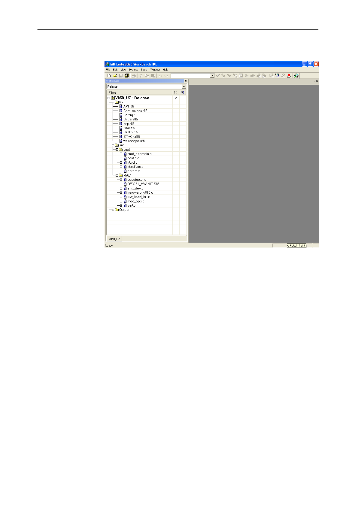
Please load the sample workspace located in the “Sample_V850SG2+ZB”
directory.
Figure 7-5 Opening the V850_UZ Sample Project
The above screen shows the sample project layout including the main system
libraries (LIB group) and source files (SRC group). The CNET group contains the
relevant application source files associated with the TCPIP libraries and the MAC
group contains all the source files associated with the IEEE 802.15.4 library.
7.3 Sample Debug session using the TK interface
Before commencing a TK interface debugging session ensure that the USB driver
has been correctly installed. The V850 ZigBeeTM Gateway Development
Platform uses a monitor program for debugging purposes. The communications
between the starter kit and the IAR C-Spy debugger running on the PC is done
via a standard UART / USB connection. The monitor program is automatically
downloaded to the starter kit during connection therefore the user does not need
to take core of the monitor program itself.
Monitor Resources
The following resources are utilised by the monitor program and cannot be used
by the user program when debugging by the TK interface.
42
User's Manual U19026EE3V0UM00
Page 43
IAR Sample Session Chapter 7
Table 7-1 Resources used by the debugging monitor
Device
V850ES/SG2
(μPD70F3281Y)
UART for
debugging
UARTD0
Additionally, please note the following points:
- Do not change the control registers of UARTD0.
- Do not change or disable the interrupt control / mask flags of
UARTD0.
- Do not change the port mode or port mode control registers for port
bits P30 and P31.
- Debugging functions like forcible break (debugger stop command)
do not operate normally in the following states where the clock
supply to UARTD0 is disabled:
• IDLE mode
• STOP mode
• Main oscillation (fx) is stopped.
Monitor Interrupt Vectors
The following interrupt vectors are used by the monitor program and cannot be
used by the user program.
Table 7-2 Monitor interupt vectors
Interrupt control
flags
UD0RMK
UD0SMK
Terminals used
P30/TxDD0
P31/RxDD0
Device
V850ES/SG2
(μPD70F3281Y)
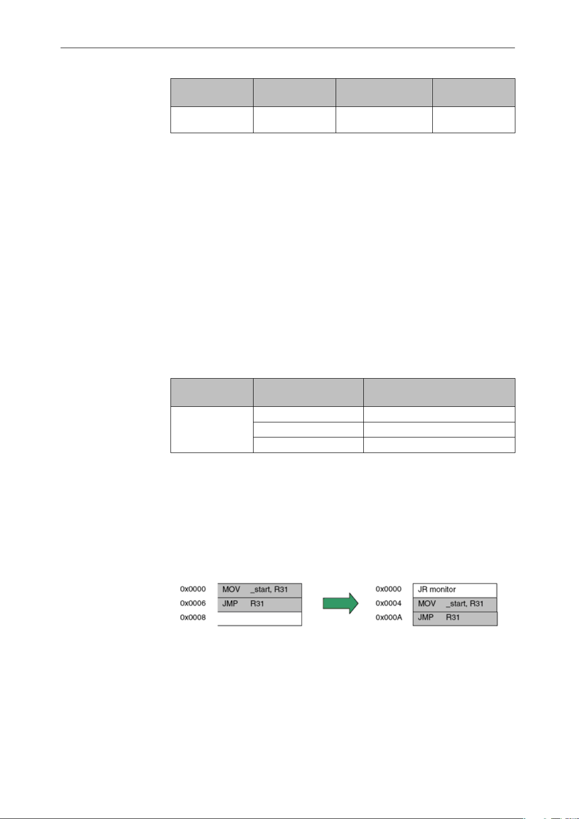
Monitor Reset Vector
When a user program is downloaded by using the IAR C-SPY debugger, the reset
vector (address 0x0000) of the user program is replaced by the one of monitor
program. The debugger moves the reset vector of the user program automatically
to address 0x0004. The correction of the relative jump address is also done
automatically by the debugger.
Example:
Figure 7-6 Monitor Reset
Memory Area reserved for monitor
Interrupt Vector
Adress
0x0060-0x0063 DBTRAP debug interrupt vector
0x02C0-0x02C3 UARTD0 receive interrupt vector
0x02B0-0x02B3 UARTD0 status interrupt vector
Function
The monitor program is located in the highest FLASH block of the V850ES/SG2
device. Only 2 kB of memory are allocated by the monitor program.
User's Manual U19026EE3V0UM00
43
Page 44

Chapter 7 IAR Sample Session
Table 7-3 Memory area reserved for monitor
Device Address range Function
V850ES/SG2
(μPD70F3281Y)
ROM: 0x5F800 - 0x5FFFF
RAM: 0xFFFF EFF0 - 0xFFFF EFFF
Reserved for monitor
program
Moreover, the monitor reserves 10 bytes of the global stack area by halting the
user program, caused by a forcible break (debugger stop command) or a software
breakpoint.
Clock operation
After releasing a reset, the monitor program sets the operation clock of the CPU
to the maximum speed of 20 MHz. The monitor program switches also to the
maximum CPU speed of 20 MHz when releasing a forcible break (debugger stop
command) or when the user program execution is stopped caused by a software
breakpoint. After the user program execution is restarted (debugger go
command), the monitor restores the previous CPU operation clock setting.
Note
Do not change the frequency of the external oscillator connected to the X1 and
X2 pins.
The baud rate calculation for UARTD0 is based on a 4 MHz input frequency,
otherwise no communication to the V850 ZigBeeTM Gateway Development
Platform board can be established.
Other limitations
The watchdog timer can not be used. Please be sure to set the option bytes of
the V850ES/SG2 device accordingly to allow the watchdog timer disable.
The forcible break (debugger stop command) can not be used when the global
interrupts were disabled by the user program (DI instruction).
Debug sessions
The debug session is done directly by connecting the V850 ZigBeeTM Gateway
Development Platform board to the host PC via the USB cable. The TK interface
of IAR manages the debug session by using the serial interface that is connected
to the USB connecter of the TK-850/SG2+UZ. When using the TK interface serial
communications via UARTD0 is disabled to prevent a clash with the monitor
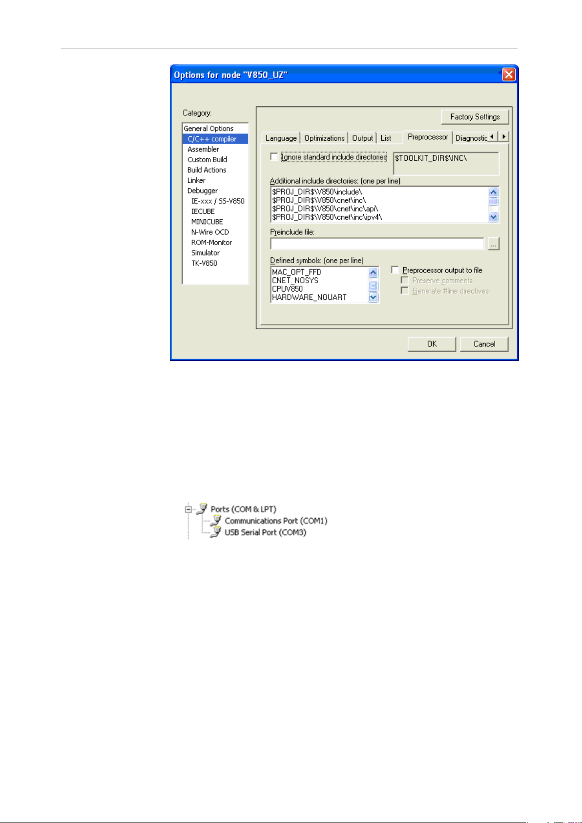
program. A pre-processor directive has been employed to ensure that the relevant
application code is disabled during a debug session. Please ensure that the
HARDWARE_NOUART pre-processor option is set in [Project] -> [Options] -> [C
\C++ Compiler] -> [Pre-processor] is set and, if necessary, rebuild the application
prior to starting the debug session.
44
User's Manual U19026EE3V0UM00
Page 45
IAR Sample Session Chapter 7
Figure 7-7 Settings of the «Pre-processor» options of the «C/C++ compiler»
Before starting a debug session, please check that the target board configuration
is set according to the settings written in the Table 3-6 "On-chip debug mode
settings for the TK-850/SG2+UZ"
If the setting is correct, then connect the TK-850/SG2+UZ board to a USB port
of your PC. Then you have to check the used communication port of the TK-V850
interface is set to the correct communications port setting. All debug targets use
port COM3, but this may be different on other PC’s. To check the actual used
communication port, please open the Windows Device Manager:
Figure 7-8 Checking the port used in the «Device manager» of Windows
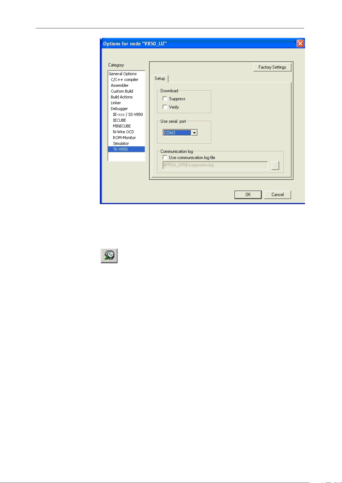
If necessary please select the correct communication port in the Embedded
Workbench menu [Project] -> [Options] -> [Debugger] -> [TK-V850]:
User's Manual U19026EE3V0UM00
45
Page 46
Chapter 7 IAR Sample Session
Figure 7-9 Configuration of the TK-V850 interface for on-chip debug mode
If all settings are correct then you can rebuild the project by selecting [Project] > [Rebuild All] and start a debug session by selecting [Project] -> [Debug], or
pressing the debugger-button in the menu bar:
Now the debugger is started and the demo project is downloaded to the TK-850/
SG2+UZ board. The progress of downloading is indicated by blue dots in the TKV850 Emulator window.
Please note that the download of larger executables can take some time.
46
User's Manual U19026EE3V0UM00
Page 47
IAR Sample Session Chapter 7
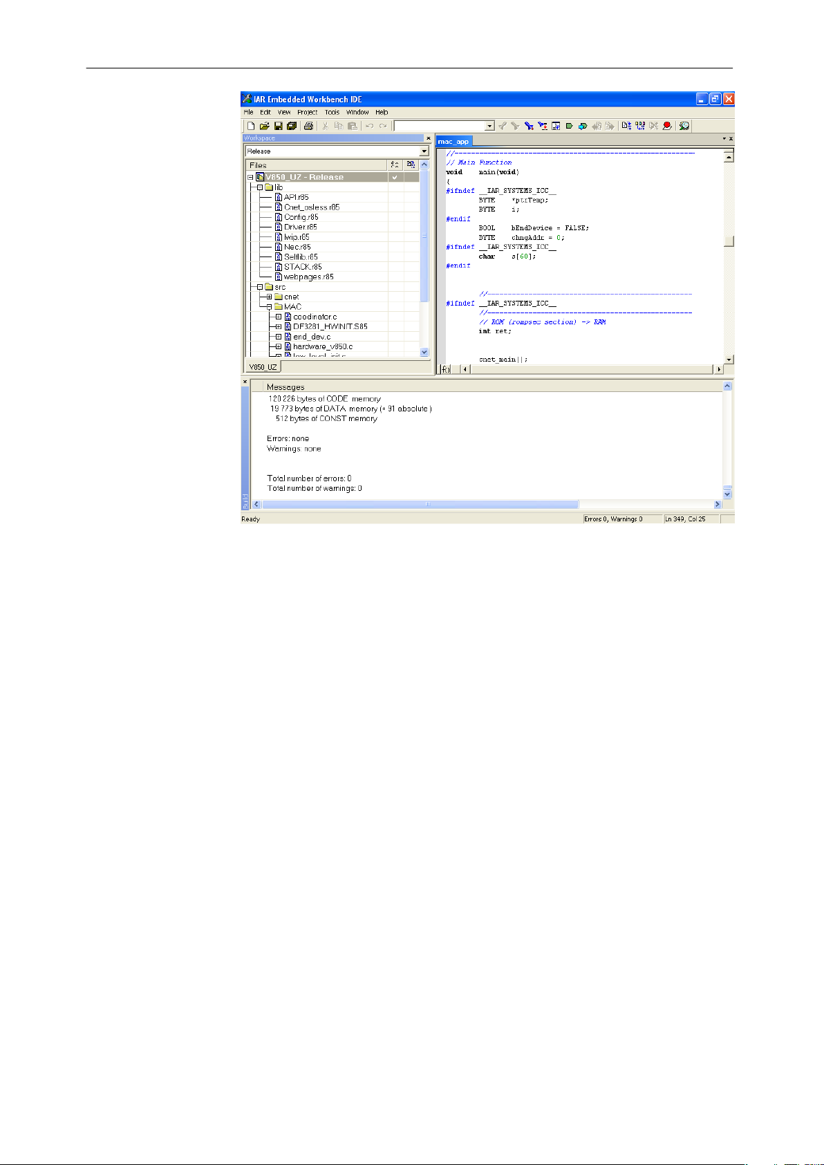
Figure 7-11 Downloading the sample application in the target device
After the download is completed, all debug features of IAR C-SPY debugger are
available, i.e. Single Stepping, Step Over/-In/-Out, Go-Execution, Breakpoints,
Register / Memory view etc.
User's Manual U19026EE3V0UM00
47
Page 48
Chapter 7 IAR Sample Session
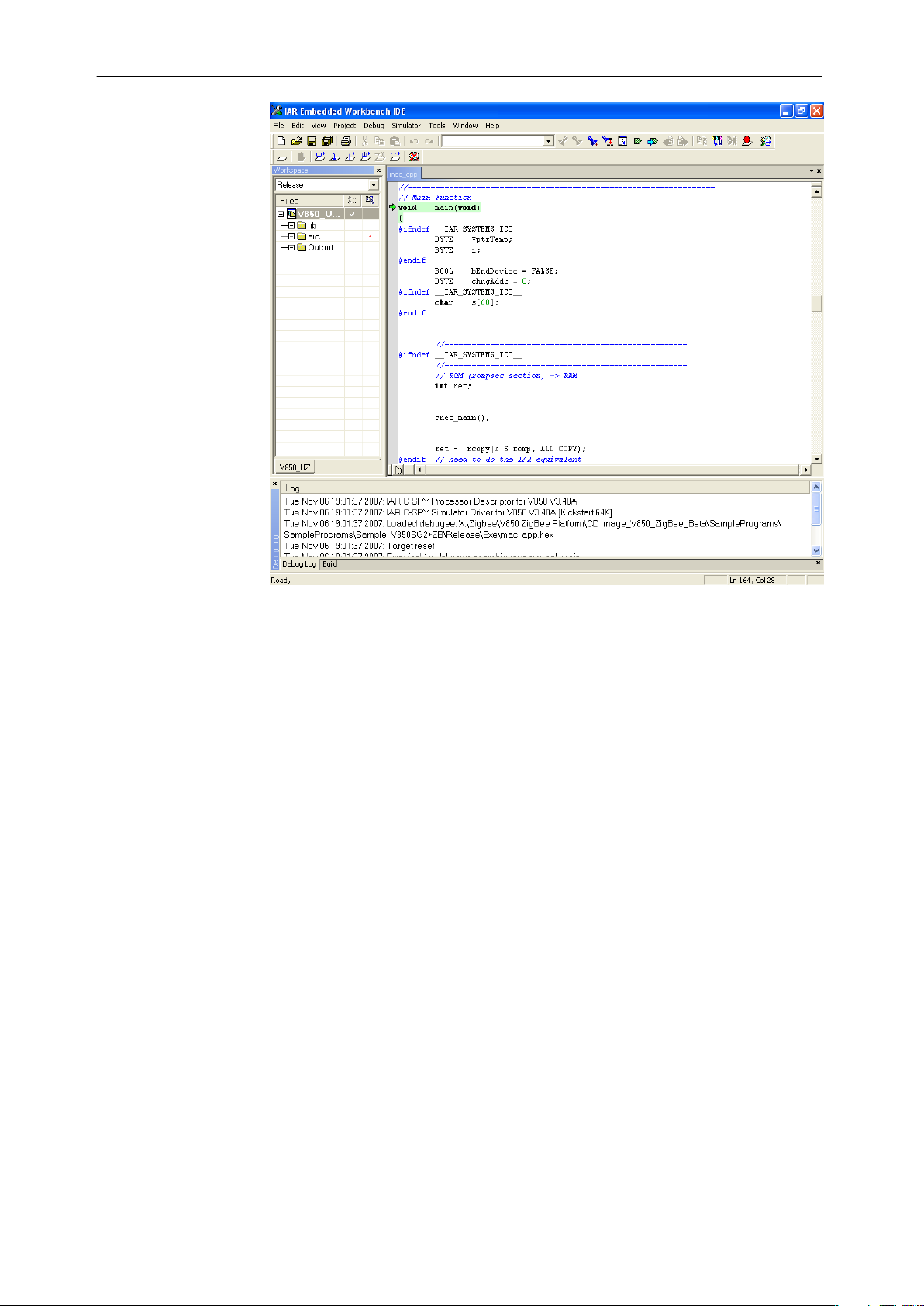
Figure 7-12 Debugging session with the Embedded Workbench C-Spy Debugger
To get more details on the debugger configuration and capabilities, please refer
to the “V850 IAR Embedded Workbench IDE User Guide” and the “V850 IAR C-
SPY® Hardware Debugger Systems User Guide”. Both manuals can be opened
directly from the Embedded Workbench help menu:
You can find the PDF-files of the manuals in the subfolder V850\doc\ of your
Embedded Workbench installation directory (e.g. C:\Program Files\IAR Systems
\Embedded Workbench 4.0\V850\doc):
• EWV850_UserGuide.ENU.pdf
• EWV850_HWDebugUserGuide.ENU.pdf
7.4 Generating a Hex file for Flash programming
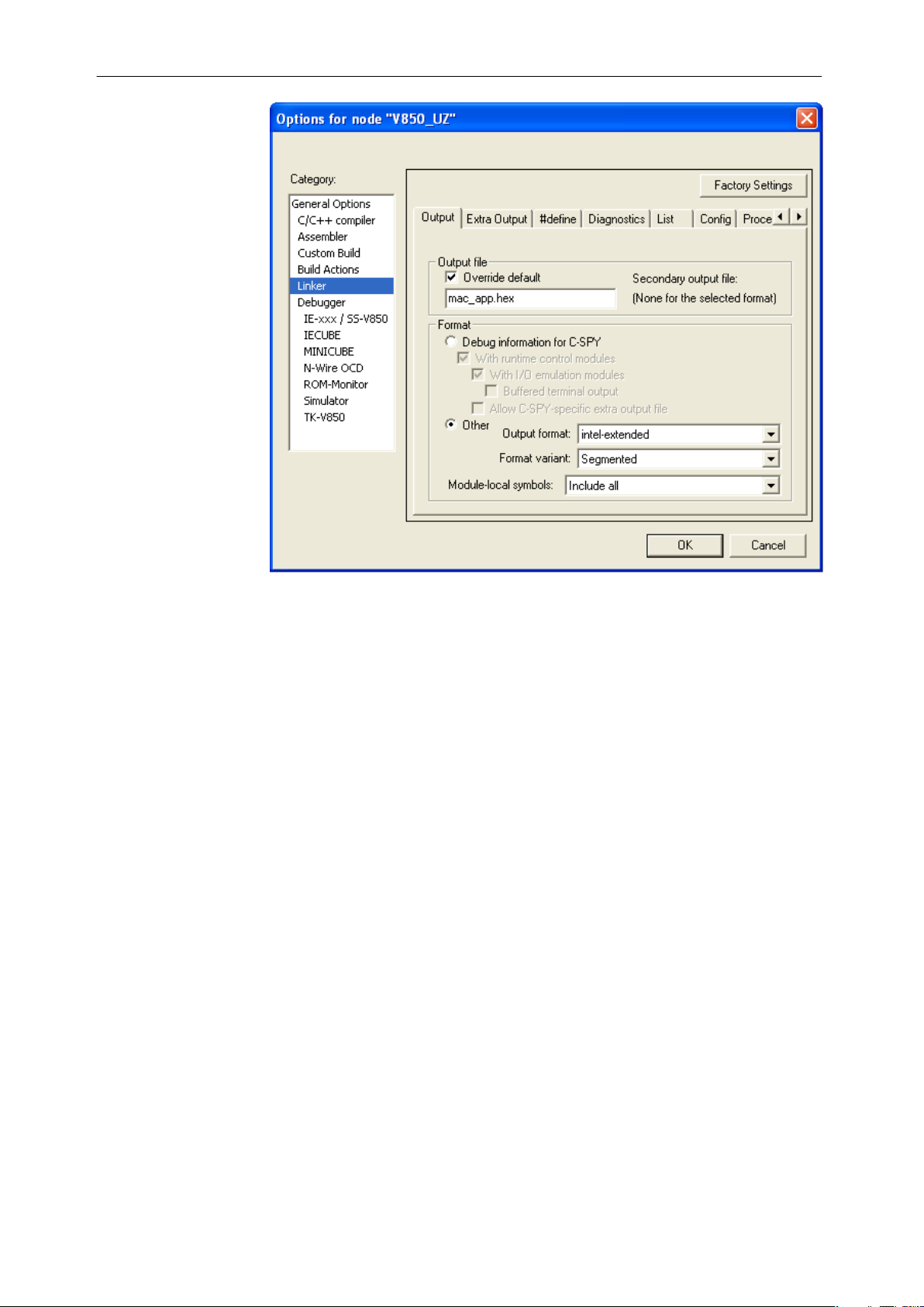
To generate a Hex-File for the FLASH–programmer please select the Target
“Release” and rebuild the project. The generated Hex-File is located in the
directory for “Executables/Libraries”. All output-file-directories are defined in the
Embedded Workbench menu [Project] -> [Options] -> [General Options] ->
[Output]:
48
User's Manual U19026EE3V0UM00
Page 49
IAR Sample Session Chapter 7
Figure 7-13 Settings to generate an HEX file output
User's Manual U19026EE3V0UM00
49
Page 50
Chapter 8 Sample Program
The V850 ZigBeeTM Gateway sample utilizes several complex libraries in order to
provide a wireless-to-Ethernet gateway solution for application development. In
this section, we will identify the key user configurable files that will allow the
solution to be tailored to the user’s application. However, it is recommended that
the users familiarize themselves with the MAC and CNET library documentation.
8.1 User configurable network Parameters
Various network parameters will always be user specific and must be tailored to
the user application; these user configurable parameters can be found in the
“config.h” header file.
8.2 Libraries
The following provides a brief overview libraries supplied with the V850
ZigBeeTM Gateway Development Platform.
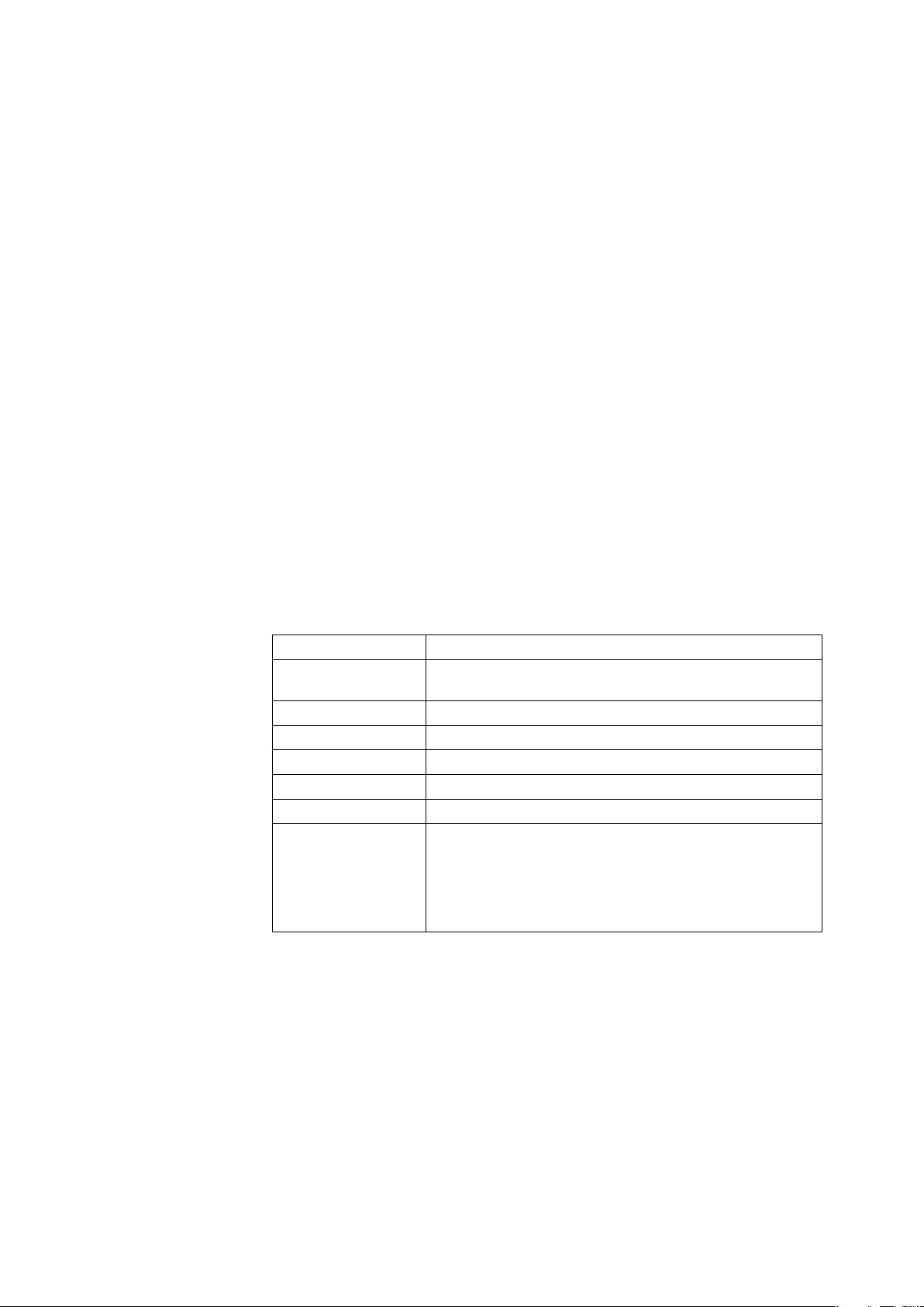
Table 8-1 Different libraries used
API.R85 API interface for the CNETTCPIP stack.
Cnet_osless.R85
Config.R85 Various system configuration utilities.
Driver.R85 Library for the Ethernet device driver.
NEC.R85 NEC Utilities and applications library.
Sellib.R85 Flash Self programming library.
Stack.R85 IEEE.802.15.4 MAC stack library.
Webpages.R85
Required to ensure correct operation of the TCPIP stack when
No RTOS is employed.
Library containing the web pages, the web pages are also
supplied as source code so that the user can modify the web
pages. Care must be taken to use the same names for the web
pages so that at link time the web page library is not called. Web
pages can generate large code sizes so care must be in the
design to ensure that the 64KB code size limit is not exceeded.
8.3 Embedded functions in Web Pages
All of the embedded functions that are called from the web interface can be found
in the file “httpdfunc.c”; should the user wish to change the functionality of the
web calls please modify the code appropriately.
50
A utility program is provided to convert web pages (see accompanying CNET user
manual) to a large data array; this data is placed in a file called “fsdata.c”. After
conversion this file needs to be modified with the following to ensure the web
pages are located in the correct segment of memory.
User's Manual U19026EE3V0UM00
Page 51

Sample Program Chapter 8
#include «lwip/def.h»
#include «api/fsdata.h»
#pragma constseg=WEBPAGES // New line at the top of the fsdata.c file
#pragma constseg=default // New line at end of the fsdata.c file
User's Manual U19026EE3V0UM00
51
Page 52
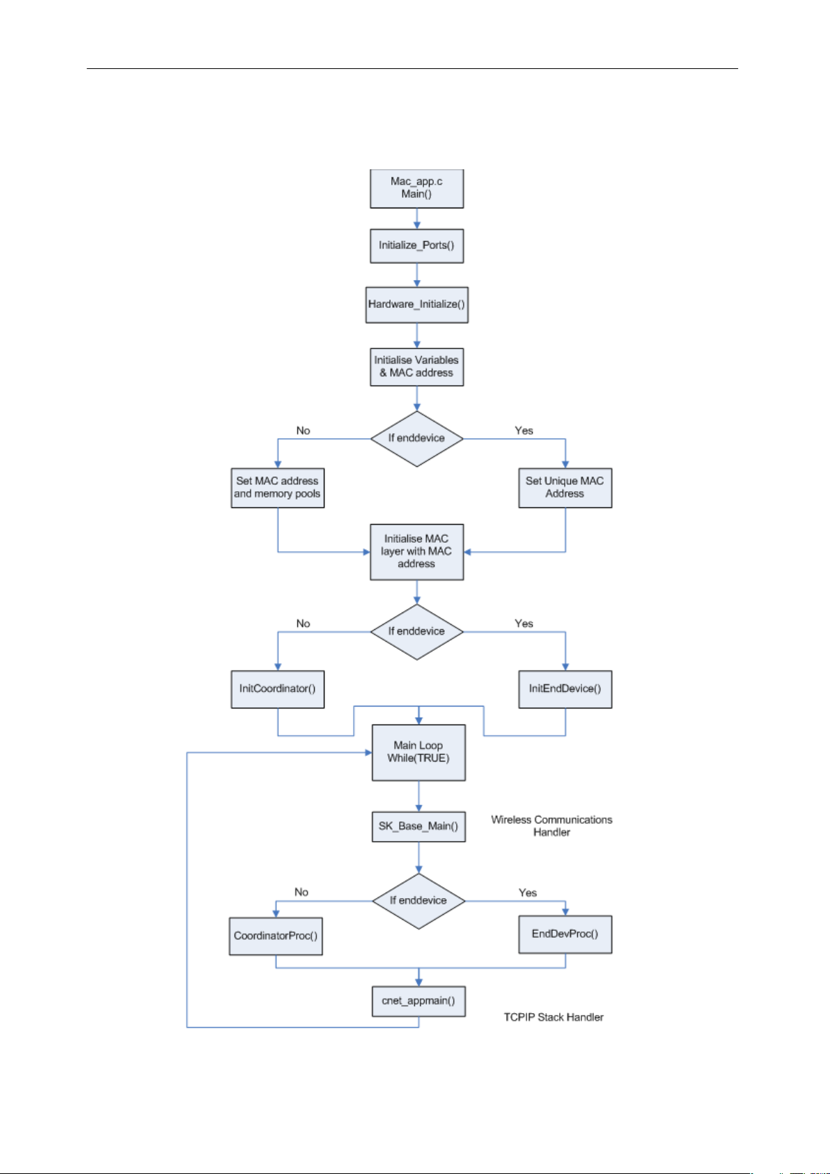
Chapter 8 Sample Program
8.4 System Initialization
52
User's Manual U19026EE3V0UM00
Page 53
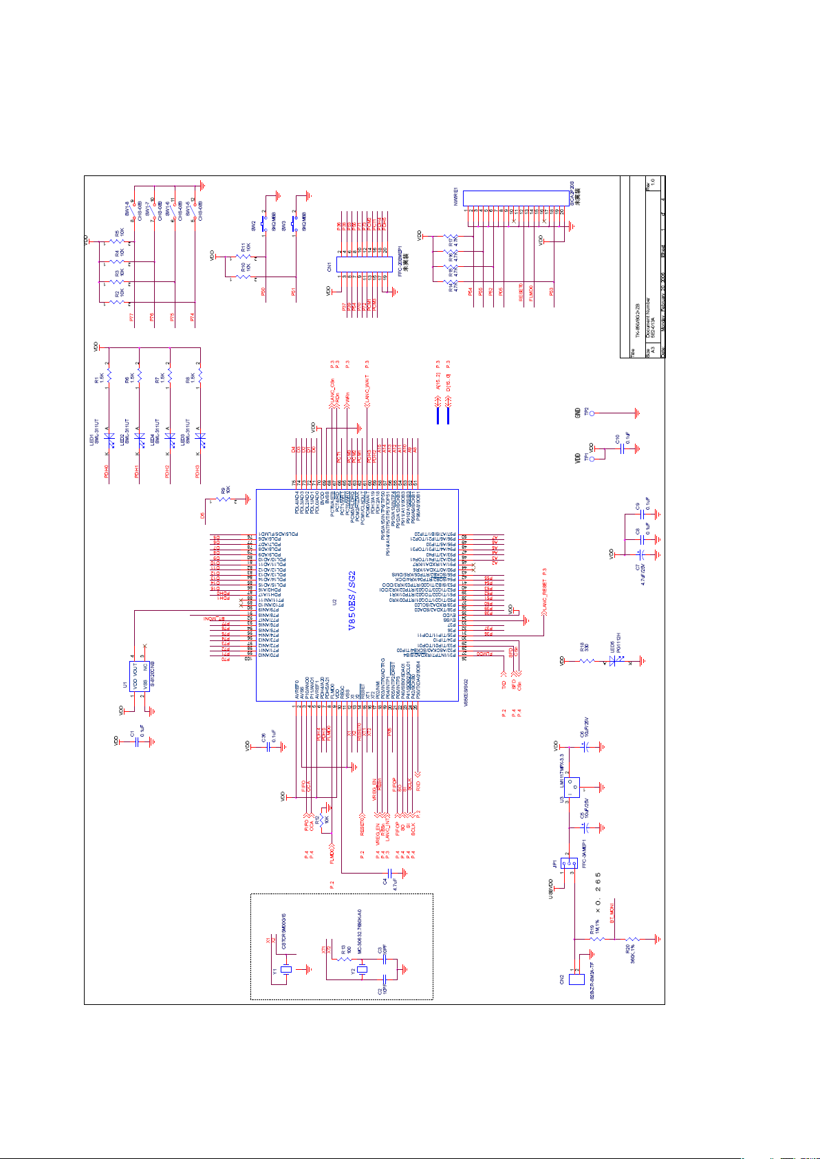
Chapter 9 Schematic Diagram TK-850/SG2+UZ
Figure 9-1 V850 ZigBee™ Gateway board schematics (1/4)
User's Manual U19026EE3V0UM00
53
Page 54
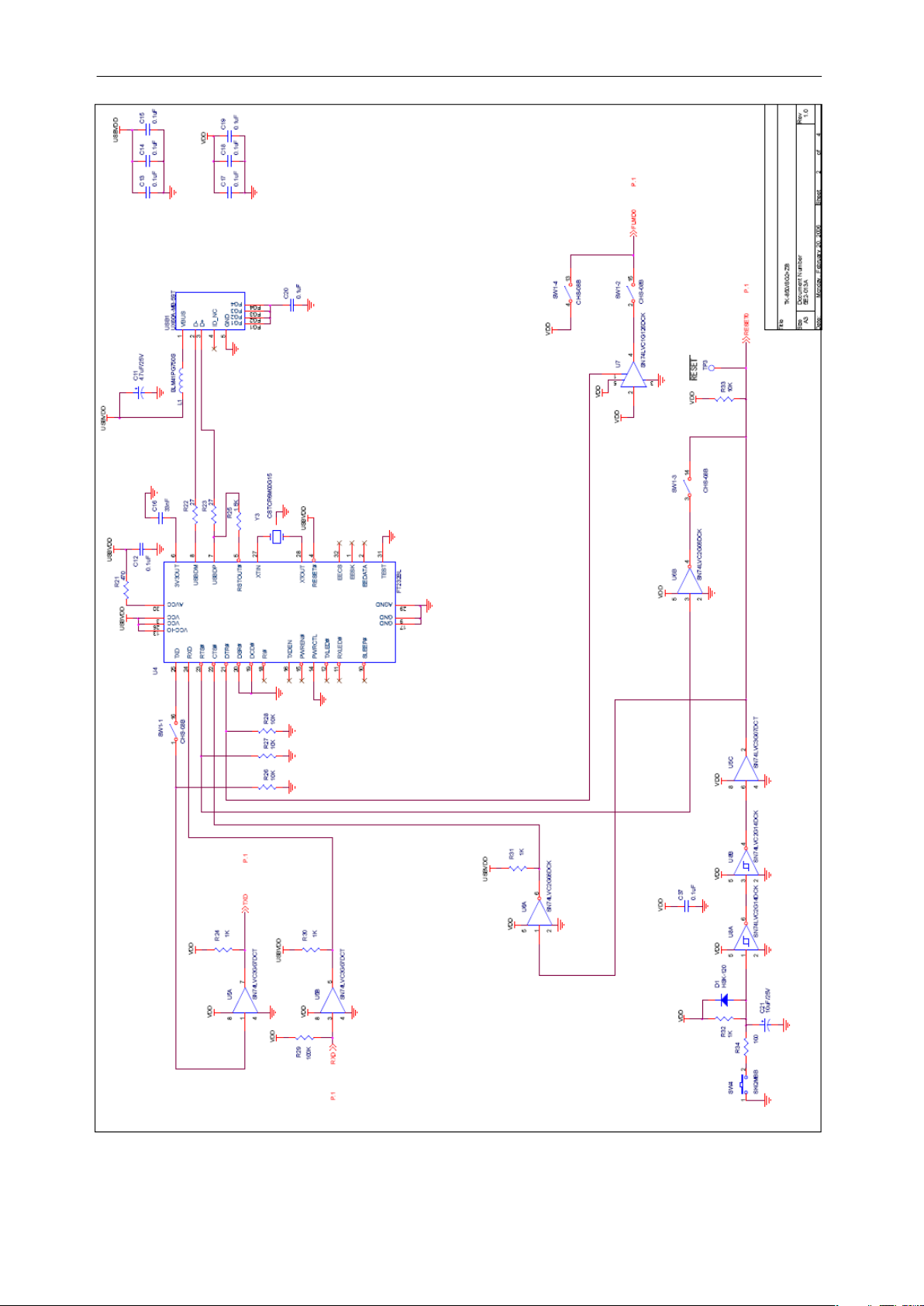
Chapter 9 Schematic Diagram TK-850/SG2+UZ
54
Figure 9-2 V850 ZigBee™ Gateway board schematics (2/4)
User's Manual U19026EE3V0UM00
Page 55
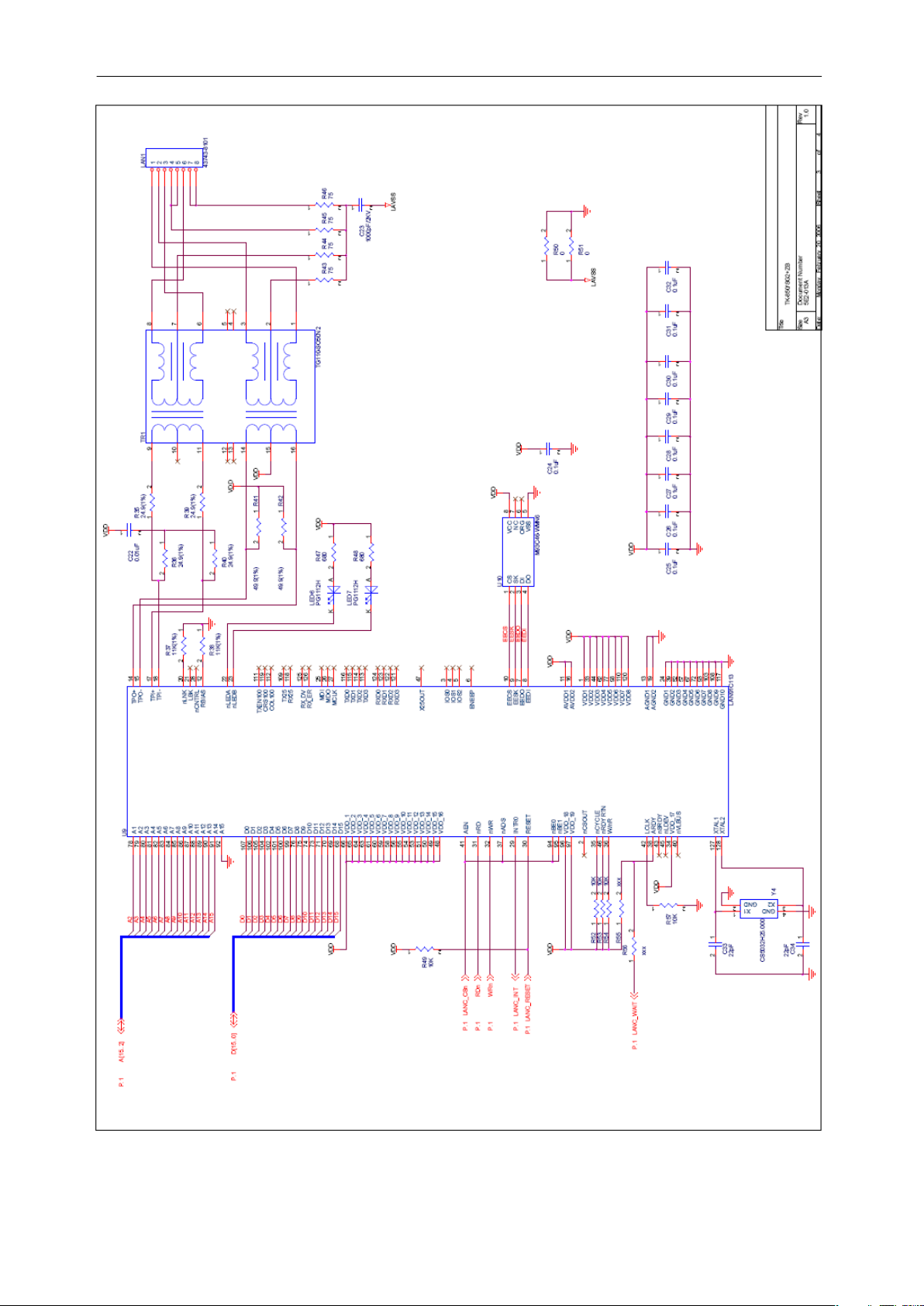
Schematic Diagram TK-850/SG2+UZ Chapter 9
Figure 9-3 V850 ZigBee™ Gateway board schematics (3/4)
User's Manual U19026EE3V0UM00
55
Page 56
Chapter 9 Schematic Diagram TK-850/SG2+UZ
56
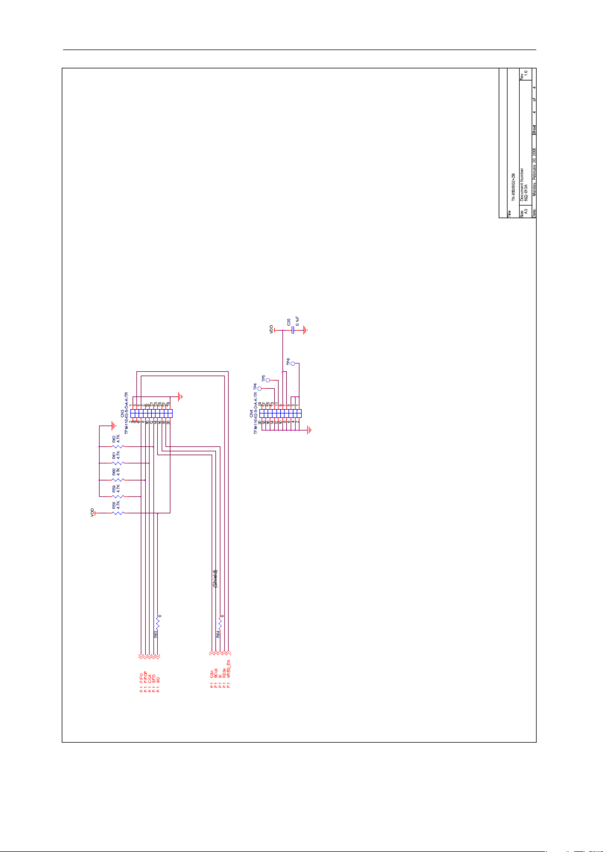
Figure 9-4 V850 ZigBee™ Gateway board schematics (4/4)
User's Manual U19026EE3V0UM00
Page 57
Chapter 10 Circuit Diagram of UZ2400 RF Board
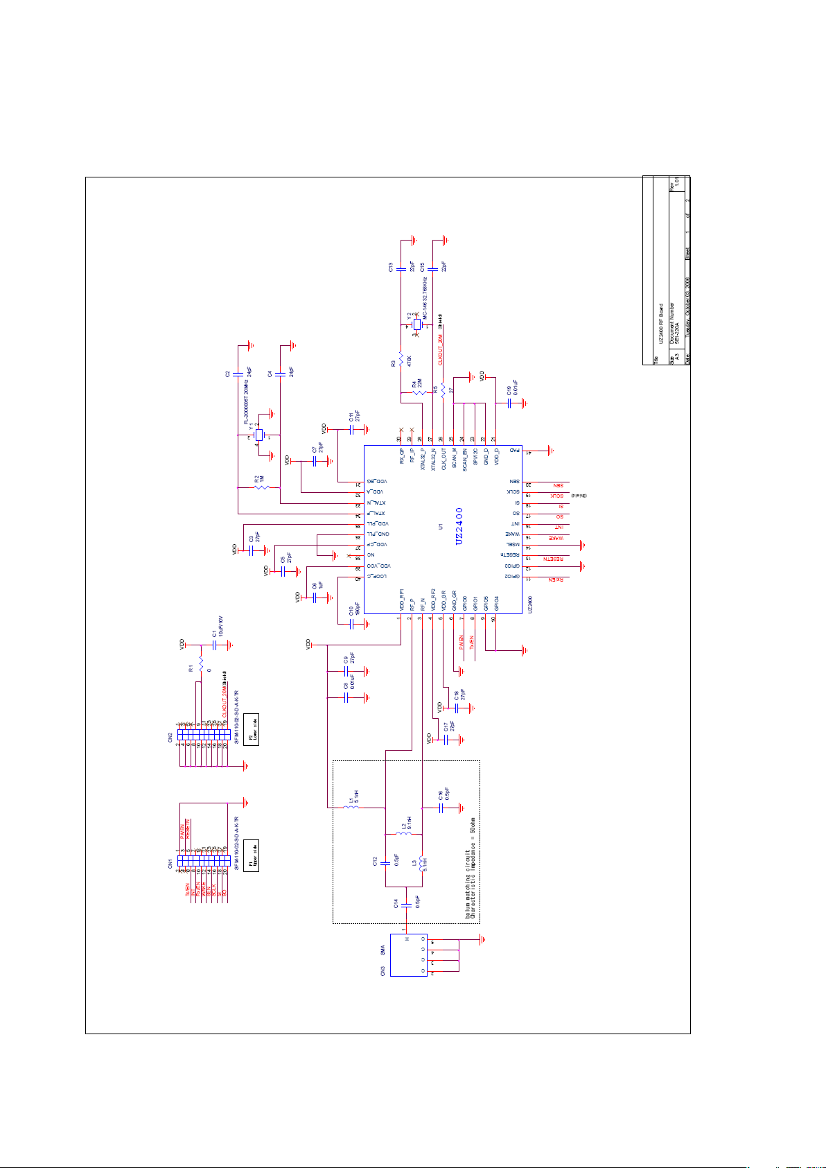
Figure 10-1 UZ2400 RF board schematics
User's Manual U19026EE3V0UM00
57
Page 58

Chapter 10 Circuit Diagram of UZ2400 RF Board
58
User's Manual U19026EE3V0UM00
Page 59

 Loading...