

Page 1

User’s Manual
IE-703040-MC-EM1
In-circuit Emulator Option Board
Target device
V850/SV1™
Document No. U14337EJ1V0UM00 (1st edition)
Date Published August 1999 N CP(K)
Printed in Japan
1999
1991©
Page 2

[MEMO]
2
User’s Manual U14337EJ1V0UM00
Page 3

V850 Family and V850/SV1 are trademarks of NEC Corporation.
Windows is either a trademark or a registered trademark of Microsoft Corporation in the United States
and/or other countries.
PC/AT is a trademark of International Business Machines Corporation.
Ethernet is a trademark of Xerox Corporation.
UNIX is a registered trademark in the United States and other countries, licensed exclusively through
X/Open Company Limited.
• The information in this document is subject to change without notice. Before using this document,
please confirm that this is the latest version.
• No part of this document may be copied or reproduced in any form or by any means without the prior written
consent of NEC Corporation. NEC Corporation assumes no responsibility for any errors which may appear in
this document.
• NEC Corporation does not assume any liability for infringement of patents, copyrights or other intellectual
property rights of third parties by or arising from use of a device described herein or any other liability arising
from use of such device. No license, either express, implied or otherwise, is granted under any patents,
copyrights or other intellectual property rights of NEC Corporation or of others.
• Descriptions of circuits, software, and other related information in this document are provided for illustrative
purposes in semiconductor product operation and application examples. The incorporation of these circuits,
software, and information in the design of the customer's equipment shall be done under the full responsibility
of the customer. NEC Corporation assumes no responsibility for any losses incurred by the customer or third
parties arising from the use of these circuits, software, and information.
M7A 98. 8
User’s Manual U14337EJ1V0UM00
3
Page 4

Regional Information
Some information contained in this document may vary from country to country. Before using any NEC
product in your application, pIease contact the NEC office in your country to obtain a list of authorized
representatives and distributors. They will verify:
•
Device availability
•
Ordering information
•
Product release schedule
•
Availability of related technical literature
•
Development environment specifications (for example, specifications for third-party tools and
components, host computers, power plugs, AC supply voltages, and so forth)
•
Network requirements
In addition, trademarks, registered trademarks, export restrictions, and other legal issues may also vary
from country to country.
NEC Electronics Inc. (U.S.)
Santa Clara, California
Tel: 408-588-6000
800-366-9782
Fax: 408-588-6130
800-729-9288
NEC Electronics (Germany) GmbH
Duesseldorf, Germany
Tel: 0211-65 03 02
Fax: 0211-65 03 490
NEC Electronics (UK) Ltd.
Milton Keynes, UK
Tel: 01908-691-133
Fax: 01908-670-290
NEC Electronics Italiana s.r.l.
Milano, Italy
Tel: 02-66 75 41
Fax: 02-66 75 42 99
NEC Electronics (Germany) GmbH
Benelux Office
Eindhoven, The Netherlands
Tel: 040-2445845
Fax: 040-2444580
NEC Electronics (France) S.A.
Velizy-Villacoublay, France
Tel: 01-30-67 58 00
Fax: 01-30-67 58 99
NEC Electronics (France) S.A.
Spain Office
Madrid, Spain
Tel: 91-504-2787
Fax: 91-504-2860
NEC Electronics (Germany) GmbH
Scandinavia Office
Taeby, Sweden
Tel: 08-63 80 820
Fax: 08-63 80 388
NEC Electronics Hong Kong Ltd.
Hong Kong
Tel: 2886-9318
Fax: 2886-9022/9044
NEC Electronics Hong Kong Ltd.
Seoul Branch
Seoul, Korea
Tel: 02-528-0303
Fax: 02-528-4411
NEC Electronics Singapore Pte. Ltd.
United Square, Singapore 1130
Tel: 65-253-8311
Fax: 65-250-3583
NEC Electronics Taiwan Ltd.
Taipei, Taiwan
Tel: 02-2719-2377
Fax: 02-2719-5951
NEC do Brasil S.A.
Electron Devices Division
Rodovia Presidente Dutra, Km 214
07210-902-Guarulhos-SP Brasil
Tel: 55-11-6465-6810
Fax: 55-11-6465-6829
J99.1
4
User’s Manual U14337EJ1V0UM00
Page 5

INTRODUCTION
Target Readers
Purpose
Organization
How to Read This Manual
This manual is intended for users who design and develop application systems using
the V850/SV1™.
The purpose of this manual is to describe the proper operation of the IE-703040-MCEM1 and its basic specifications.
This manual is divided into the following parts.
• Overview
• Names and functions of components
• Cautions
It is assumed that the reader of this manual has general knowledge in the fields of
electrical engineering, logic circuits, and microcontrollers.
The IE-703040-MC-EM1 is used connected to the IE-703002-MC in-circuit emulator.
This manual explains the basic setup procedure and switch settings of the IE703002-MC when it is connected to the IE-703040-MC-EM1. For the names and
functions of parts, and the connection of elements, refer to the
Manual (U11595E)
.
IE-703002-MC User’s
To learn about the basic specifications and operation methods
Read this manual in the order of the
→
CONTENTS
.
Conventions
Terminology
To learn the operation methods and command functions, etc., of the IE-703002-MC
and IE-703040-MC-EM1
Read the user’s manual of the debugger (sold separately) that is used.
→
Note: Footnote for item marked with
Note
in the text
Caution: Information requiring particular attention
Remark: Supplementary information
Numeral representation: Binary … xxxx or xxxxB
Decimal … xxxx
Hexadecimal … xxxxH
Prefix indicating the power of 2 (address space, memory capacity):
10
K (kilo): 2
M (mega): 220 = 1024
= 1024
2
The meanings of terms used in this manual are listed below.
Target device The device that is targeted for emulation.
Target system The system (user-built system) that is targeted for debugging. This
includes the target program and user-configured hardware.
User’s Manual U14337EJ1V0UM00
5
Page 6

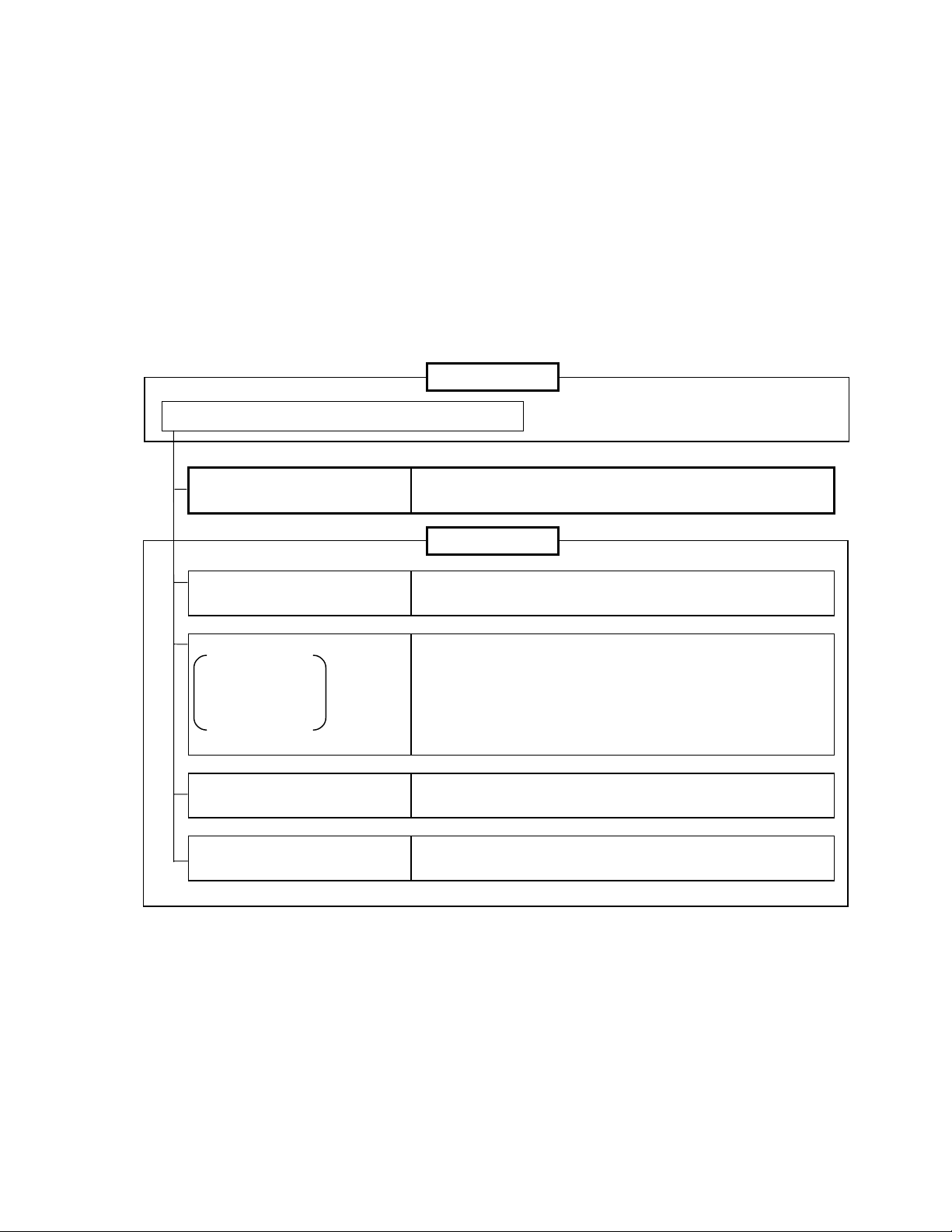
Related Documents
When using this manual, refer to the following manuals.
The related documents indicated in this publication may include preliminary versions.
However, preliminary versions are not marked as such.
{
Documents related to development tools (user’s manuals)
Document Name Document
Number
IE-703002-MC U11595E
IE-703040-MC-EM1 This manual
CA830, CA850 (C Compiler package)
CA850 (C Compiler package) Assembly Language U13828E
ID850 (Ver.1.31) (Integrated debugger) Operation Windows-based U13716E
ID850 (Ver.2.00 or more)
(Integrated debugger)
SM850 (Ver.2.00 or more)
(System simulator)
RD850 (Task debugger)
RD850 (Ver.3.0) (Task debugger) Windows-based U13737E
RD850 Pro (Ver.3.0) (Task debugger) Windows-based U13916E
AZ850 (System performance analyzer) U11181E
Note
Operation Windows-based U13998E
C language U13997E
Project manager U13996E
Operation Windows-based U14217E
Operation Windows-based U13759E
Basics U13430ERX850 (Real-time OS)
Installation U13410E
Fundamental U13773ERX850 Pro (Real-time OS)
Installation U13774E
Windows-based U11158E
For ID850 (Ver. 1.31 only)
Note
6
User’s Manual U14337EJ1V0UM00
Page 7

CONTENTS
CHAPTER 1 OVERVIEW.........................................................................................................................11
1.1 Hardware Configuration............................................................................................................................... 11
1.2 Features (When Connected to IE-703002-MC)...........................................................................................12
1.3 Function Specifications (When Connected to IE-703002-MC).................................................................. 12
1.4 System Configuration ..................................................................................................................................13
1.5 Contents in Carton.......................................................................................................................................14
1.6 Connection between IE-703002-MC and IE-703040-MC-EM1................................................................ 16
CHAPTER 2 NAMES AND FUNCTIONS OF COMPONENTS................................................................19
2.1 Component Names and Functions of IE-703040-MC-EM1........................................................................ 19
2.2 Clock Settings............................................................................................................................................... 21
2.2.1 Main system clock setting ................................................................................................................ 21
2.2.2 Subsystem clock setting................................................................................................................... 22
2.3 Illegal Access Detection ROM Setting........................................................................................................ 23
2.4 CPU Operation Voltage Range Switching Setting..................................................................................... 23
CHAPTER 3 FACTORY SETTINGS........................................................................................................25
CHAPTER 4 CAUTIONS..........................................................................................................................27
4.1 VDD and BVDD of Target System................................................................................................................... 27
4.2 NMI Signal.....................................................................................................................................................28
4.3 VPP Signal......................................................................................................................................................28
4.4 NMI Signal Mask Function........................................................................................................................... 29
4.5 Bus Interface Pin..........................................................................................................................................29
APPENDIX PACKAGE DRAWINGS.........................................................................................................31
User’s Manual U14337EJ1V0UM00
7
Page 8

LIST OF FIGURES
Figure No. Title Page
1-1 System Configuration............................................................................................................................................13
1-2 Contents in Carton.................................................................................................................................................14
1-3 Accessories........................................................................................................................................................... 15
1-4 Connection between IE-703002-MC and IE-703040-MC-EM1..............................................................................17
2-1 IE-703040-MC-EM1...............................................................................................................................................19
4-1 Schematic Diagram of Power Supply Acquisition..................................................................................................27
4-2 NMI Signal Flow Path............................................................................................................................................28
4-3 VPP Signal Flow Path.............................................................................................................................................28
8
User’s Manual U14337EJ1V0UM00
Page 9

LIST OF TABLES
Table No. Title Page
2-1 Main System Clock Setting ...................................................................................................................................21
2-2 Subsystem Clock Setting ......................................................................................................................................22
2-3 JP1 Setting in IE-703002-MC................................................................................................................................23
2-4 JP3 and JP4 Setting in IE-703002-MC.................................................................................................................. 23
4-1 Bus Interface Pin Operation List............................................................................................................................29
User’s Manual U14337EJ1V0UM00
9
Page 10

[MEMO]
10
User’s Manual U14337EJ1V0UM00
Page 11
CHAPTER 1 OVERVIEW
The IE-703040-MC-EM1 is an option board for the IE-703002-MC in-circuit emulator. By connecting the IE703040-MC-EM1 and IE-703002-MC, hardware and software can be debugged efficiently in system development
using the V850/SV1.
In this manual, the basic setup procedure and switch settings of the IE-703002-MC when using the IE-703040-MCEM1 are described. For the names and functions of the parts of the IE-703002-MC, and for the connection of
elements, refer to the
IE-703002-MC User’s Manual (U11595E)
.
1.1 Hardware Configuration
Optional hardware
Optional hardware
In-circuit emulator (I E-703002-MC)
Notes 1.
Option board
(IE-703040-MC-EM1)
Extension probe (SC-176SD
PC interface board
IE-70000-xx-IF-B
IE-70000-xx-IF-C
IE-70000-PCI-IF
IE-70000-CD-IF-A
Network module
(IE-70000-MC-SV3)
Power adapter
(IE-70000-MC-PS-B)
Note 1
)
By adding this board, the I E -703002-M C can be used as in-circuit
emulator for V850/SV1.
Optional hardware
General-purpose extension probe made by TOKYO ELETECH
CORPORATION
This board is used to connect the IE-703002-MC to a personal computer.
This board is inserted in the ex pansion slot of the personal c om puter.
xx: 98 (for PC-9800 series C bus)
PC (for IBM PC/AT™ or compatibles ISA bus)
IE-70000-PCI-IF: for PCI bus
IE-70000-CD-IF-A: for PCM CIA socket
This module is used when a workstation controls the IE -703002-M C v i a
Ethernet™.
AC adapter for in-circuit em ul at or m ade by NEC Corporation.
For further information, contact Daimaru Kogyo Co., Ltd
Tokyo Electronics Department (TEL +81-3-3820-7112)
Osaka Electronics Department (TEL +81-6-6244-6672)
Cannot be used for PC98-NX series
2.
Note 2
Note 2
.
User’s Manual U14337EJ1V0UM00
11
Page 12

CHAPTER 1 OVERVIEW
1.2 Features (When Connected to IE-703002-MC)
Maximum operating frequency: 20 MHz (at 3.3 to 5.0-V operation)
{
Extremely lightweight and compact
{
Higher equivalence with target device can be achieved by omitting buffer between signal cables.
{
The following pins can be masked.
{
RESET, NMI, WAIT, HLDRQ
Two methods of connection to target system:
{
• Pod tip direct connection (For information on the pod, refer to the
• Attach an extension probe (sold separately) to the pod tip for connection
The dimensions of the IE-703040-MC-EM1 are as follows.
{
Parameter Value
Power consumption (Max. value at 3.3-V supply vol t age)
External dimensions
(Refer to
DRAWINGS
Weight 160 g
APPENDIX PACKAGE
)
Height 15 mm
Length 194 mm
Width 96 mm
0.35 W (at 20-MHz operation frequency )
IE-703002-MC User’s Manual (U11595E)
)
Note
10.35 W when IE-703002-MC connected to IE-703040-MC-EM1
Note
1.3 Function Specifications (When Connected to IE-703002-MC)
Parameter Specification
Emulation memory capac i ty
Coverage memory capacity for
execution/pass detection
Coverage memory capacity for
memory access detection
Coverage memory capacity for
branching entry number counting
Caution Some of the functions may not be supported, depending on the debugger used.
Internal ROM 256 Kbytes
External
memory
Internal ROM 256 Kbytes
External
memory
External memory 1 Mbyte
Internal ROM 256 Kbytes
External
memory
In ROM-less mode 2 Mbytes
When using iROM 1 Mbyte
In ROM-less mode 2 Mbytes
When using iROM 1 Mbyte
In ROM-less mode 2 Mbytes
When using iROM 1 Mbyte
12
User’s Manual U14337EJ1V0UM00
Page 13

CHAPTER 1 OVERVIEW
1.4 System Configuration
The system configuration when connecting the IE-703002-MC to the IE-703040-MC-EM1 and a personal computer
(PC-9800 series or PC/ATTM (or compatibles)) is shown below.
Figure 1-1. System Configuration
<13>
<2>
<1>
<14>
For PC-9800 series
<12>
<4>
<3>
For PC/AT or
compatibles
<5>
<6>
[Magnified drawing: example of use of
connector for target connection]
<8>
<9>
<10>
<11>
Remark
<1> Personal computer (PC-9800 series or PC/AT or compatibles)
<2> Debugger (sold separately)
<3> PC interface board
(IE-70000-98-IF-B/IE-70000-98-IF-C, IE-70000-PC-IF-B/IE-70000-PC-IF-C: sold separately)
<4> PC interface cable (included with IE-703002-MC)
<5> In-circuit emulator (IE-703002-MC: sold separately)
<6> In-circuit emulator option board (IE-703040-MC-EM1)
<7> External logic probe (included with IE-703002-MC)
<8> Socket for target connection (YQSOCKET176SDN: sold separately)
<9> Extension probe (SC-100SD: sold separately)
<10> Connector for emulator connection (YQPACK176SD: included)
<11> Connector for target connection (NQPACK176SD: included)
<12> Power adapter (IE-70000-MC-PS-B : sold separately)
<13> AC100-V power cable (sold separately: included with IE-70000-MC-PS-B)
<14> AC220-V power cable (sold separately: included with IE-70000-MC-PS-B)
<10>
<11>
<7>
Target
system
Target system
User’s Manual U14337EJ1V0UM00
13
Page 14

CHAPTER 1 OVERVIEW
1.5 Contents in Carton
The carton of the IE-703040-MC-EM1 contains a main unit, guarantee card, packing list, and accessory bag.
Make sure that the accessory bag contains this manual and the connector accessories. If there are missing or
damaged items, please contact an NEC sales representative or an NEC distributor.
Figure 1-2. Contents in Carton
<1> IE-703040-MC-EM1
<4> Packing list
<3> Guarantee card
<2> Accessory bag
14
<1> IE-703040-MC-EM1 × 1
<2> Accessory bag × 1
<3> Guarantee card × 1
<4> Packing list × 1
User’s Manual U14337EJ1V0UM00
Page 15

CHAPTER 1 OVERVIEW
Check that the accessory bag contains this manual, an accessory list (× 1), and the following accessories.
(a) Connector for target connection (NQPACK176SD) × 1
(including NQGUIDE × 3, driver × 1)
(b) Connector for emulator connection (YQPACK176SD) × 1
(including YQGUIDE × 4)
(c) Crystal oscillator (20-MHz, 8-pin type)
(d) Plastic screws × 4
(including nuts and washer × 4)
(e) Jumper contact × 1
Figure 1-3. Accessories
(a) Connector for target connection (b) Connector for emulator connection
NQPACK176SD
(Side view)
NQGUIDE Driver
YQPACK176SD
(Side view)
YQGUIDE
(c) Crystal oscillator (d) Plastic screws
(e) Jumper contact
Caution NQPACK176SD is intended for laboratory use such as program development and evaluation.
User’s Manual U14337EJ1V0UM00
15
Page 16

CHAPTER 1 OVERVIEW
1.6 Connection between IE-703002-MC and IE-703040-MC-EM1
The procedure for connecting the IE-703002-MC and IE-703040-MC-EM1 is described below.
Caution Connect carefully so as not to break or bend connector pins.
<1> Remove the pod cover (upper and lower) of the IE-703002-MC.
<2> Replace the crystal oscillator mounted in the pod of the IE-703002-MC with the crystal oscillator supplied (20
MHz) or an arbitrary oscillator (user’s frequency).
<3> Set the PGA socket lever of the IE-703040-MC-EM1 to the OPEN position as shown in Figure 1-4 (b).
<4> Connect the IE-703040-MC-EM1 to the PGA socket at the back of the IE-703002-MC pod (refer to Figure 1-4
(c)). When connecting, position the IE-703002-MC and IE-703040-MC-EM1 so that they are horizontal.
<5> Set the PGA socket lever of the IE-703040-MC-EM1 to the CLOSE position as shown in Figure 1-4 (b).
<6> Set the IE-703002-MC pod jumpers (JP1 to JP4).
Open JP1 and JP3 (Remove the jumper contact and attach the removed jumper contact to one of the jumper
pins to avoid losing it.)
Retain the factory settings of JP2 (pins 1 and 2 shorted, and pins 5 and 6 shorted).
Short pins 2 and 3 of JP4.
<7> Fix the IE-703040-MC-EM1 between the IE-703002-MC pod covers (upper and lower) with the plastic screws
(supplied with the IE-703002-MC).
<8> Fix the IE-703002-MC pod cover (upper) end with nylon rivets.
Remark
For the JP1 setting, refer to
to
2.4 CPU Operation Voltage Range Switch Setting
2.3 Illegal Access Detection ROM Setting
. For JP3 and JP4, refer
.
16
User’s Manual U14337EJ1V0UM00
Page 17

CHAPTER 1 OVERVIEW
Figure 1-4. Connection between IE-703002-MC and IE-703040-MC-EM1 (1/2)
(a) Overview
Nylon rivets
IE-703002-MC
(b) PGA Socket Lever of IE-703040-MC-EM1
Upper cover
Nut
Washer
IE-703040-MC-EM1
Lower cover
Plastic screw
CLOSE
OPEN
User’s Manual U14337EJ1V0UM00
17
Page 18

CHAPTER 1 OVERVIEW
Figure 1-4. Connection between IE-703002-MC and IE-703040-MC-EM1 (2/2)
(c) Connecting part (IE-703040-MC-EM1)
Pin A1 position
18
: Insertion guide
: IE-703002-MC insertion area
User’s Manual U14337EJ1V0UM00
Page 19

CHAPTER 2 NAMES AND FUNCTIONS OF COMPONENTS
This chapter describes the names, functions, and switch settings of components in the IE-703040-MC-EM1. For
the details of the pod, jumper, and switch positions, etc., refer to the
2.1 Component Names and Functions of IE-703040-MC-EM1
Figure 2-1. IE-703040-MC-EM1
(a) Top view (b) Bottom view
Direction of pin 1 of connector
for target connection
V
1
9
TP12
2
JP6
10
CPLD
PP
LED
1
1
JP5
JP3
JP1
3
717
1
JP4
3
1
JP2
3
V850/SV1
I/O chip
TP5
IE-703002-MC User’s Manual (U11595E)
Direction of pin 1 of connector
for target connection
Connector for target connection
.
TP11
PROM
IE-703002-MC connection
Connector for
User’s Manual U14337EJ1V0UM00
19
Page 20

CHAPTER 2 NAMES AND FUNCTIONS OF COMPONENTS
(1) TEST pins (TP5, TP11, TP12)
These are pins used for testing the analog signals of the standalone emulator.
TP 5: GND
•
TP 11: GND
•
TP 12: GND
•
(2) JP1
This is a pin board for product check. Mount nothing on JP1.
(3) JP2, JP4
These are pin boards for product check. Use and retain the factory settings (pins 2 and 3 shorted) (For details,
refer to
2.2 Clock Settings
)
(4) JP3
This is a pin board for supplying the subsystem clock. (For details, refer to
2.2 Clock Settings
)
(5) JP5
This is a jumper for switching the main system clock supply source.
(6) JP6
This is a pin board for product check. Use and retain the factory settings (pins 1 and 2 shorted).
(7) LED
LED for V
ON: Voltage is applied to V
OFF: Voltage is not applied to V
PP
PP
PP
(8) Connector for IE-703002-MC connection
This is a connector for connecting with the IE-703002-MC.
(9) Connector for target connection
This is a connector for connecting with the target system or the extension probe.
20
User’s Manual U14337EJ1V0UM00
Page 21

CHAPTER 2 NAMES AND FUNCTIONS OF COMPONENTS
2.2 Clock Settings
This section describes the clock settings.
For the position of the JP1 and JP2 in the IE-703040-MC-EM1, refer to Figure 2-1.
For the jumper switch position in the IE-703002-MC, refer to the
IE-703002-MC User’s Manual (U11595E)
2.2.1 Main system clock setting
Table 2-1. Main System Clock Setting
.
Environment
When using
emulator as
standalone unit
When using
emulator with
target system
Note
The target clock supports only an oscillator (X2 cannot be used because it is not connected in the
emulator).
Clock input by resonator is not supported.
Clock Supply Method
Internal clock
Internal clock
Target clock
Note
IE-703040-MC-EM1 Setting IE-703002-MC S et tingEmulator Use
JP1 SW1 SW2 JP2
12
12
12
3
3
3
ON
ON
7
8
1
2
User’s Manual U14337EJ1V0UM00
21
Page 22

CHAPTER 2 NAMES AND FUNCTIONS OF COMPONENTS
2.2.2 Subsystem clock setting
Table 2-2. Subsystem Clock Setting
Environment
When using emulator as
standalone unit
When using emulator with
target system
Notes 1.
The internal clock does not support the clock input by an oscillator.
The target clock supports only an oscillator (XT2 cannot be used because it is not connected in the
2.
emulator).
Clock input by oscillator is not supported.
To use a subsystem clock frequency other than 32.768 kHz, remove the clock module on JP3 and
3.
mount any oscillator.
The specifications of JP3 are as follows.
Target
XT1
Clock Supply Method
Internal clock
Internal clock
Target clock
Note 1
Note 1
Note 2
XT1
V850/SV1
I/O chip
IE-703040-MC-EM1 SettingEmulator Use
JP3
Oscillator mounted (a 32.768-kHz osc illat or is mounted when
shipped)
Oscillator mounted (a 32.768-kHz osc illat or is mounted when
shipped)
Pins 3 and 4 of JP3 are shorted
Note 3
Note 3
Note 4
12345
JP3
67
XT2
22
Prepare the short pin.
4.
1
GND GNDC1 C2XT1 XT2TG
User’s Manual U14337EJ1V0UM00
7
Page 23

CHAPTER 2 NAMES AND FUNCTIONS OF COMPONENTS
2.3 Illegal Access Detection ROM Setting
If using the IE-703002-MC for an in-circuit emulator for the V850/SV1 by connecting the IE-703040-MC-EM1, set
JP1 of the IE-703002-MC as follows.
Table 2-3. JP1 Setting in IE-703002-MC
JP1 Description
Note
Open
Illegal access detection ROM (mounted on IE-703040-MC-EM 1) f or V850/SV1 is
used.
Note
When JP1 is set open, keep the removed jumper contact attached to one pin
JP1
as shown in the drawing on the right.
Jumper
contact
2.4 CPU Operation Voltage Range Switching Setting
If using the IE-703002-MC for an in-circuit emulator for the V850/SV1 by connecting the IE-703040-MC-EM1, set
JP3 and JP4 of the IE-703002-MC as follows.
Table 2-4. JP3 and JP4 Setting in IE-703002-MC
JP3, JP4 Description
JP3
(Open)
JP4
The operation voltage range of the IE-703002-MC is to 2 to 3.6 V
1
2
The operation voltage range of the target system is 2 to 4.5 V.
1
(Use this setting s i nce the operation voltage range of the V 850/ SV1 is 2 to 3.6 V.)
2
3
Caution By settings of JP3, JP4 above, when the power supply of the target system is on, the IE-703002-
MC operates at the same voltage as the target system.
The IE-703002-MC always operates at 3.3 V when the power supply of the target system is off and
using emulator as standalone unit.
User’s Manual U14337EJ1V0UM00
23
Page 24

[MEMO]
24
User’s Manual U14337EJ1V0UM00
Page 25

CHAPTER 3 FACTORY SETTINGS
Item Description Remark
JP1
JP2
Oscillator not mounted
12
3
Pin board for product check
Jumper switch for product check
JP3 Oscillator mounted 32.768-kHz clock supplied for subsystem clock
JP4
JP5
JP6
12
12
2
1
3
3
Jumper switch for product check
Internal clock used for main system clock
Jumper switch for product check
10
9
User’s Manual U14337EJ1V0UM00
25
Page 26

[MEMO]
26
User’s Manual U14337EJ1V0UM00
Page 27

CHAPTER 4 CAUTIONS
4.1 V
DD
and BVDD of Target System
(1) BVDD in the target system is not connected to BVDD in the evaluation chip in the IE-703002-MC.
The IE-703002-MC uses BVDD of the target system for the following purposes:
Power ON/OFF detection of target system
•
BVDD emulation of target system
•
(2) When the voltage of the target system is 1 V or higher, the evaluation chip in the emulator operates using the
supply of VDD from the target system. The power consumption is equivalent to that of the V850/SV1.
(3) When the voltage of the target system is lower than 1 V, the emulator recognizes the target system power is off
and operates at 3.3 V.
Figure 4-1. Schematic Diagram of Power Supply Acquisition
Target system
BV
IE-703040-MC-EM1
DD
V850/SV1
I/O chip
IE-703002-MC
Target voltage
emulation
BV
DD
BV
DD
V
DD
Relay
≥
1 V
BV
DD
< 1 V
Evaluation chip
User’s Manual U14337EJ1V0UM00
27
Page 28

CHAPTER 4 CAUTIONS
4.2 NMI Signal
The input signal (NMI signal) from the target system is delayed (tpD = 0.25 ns (TYP.)) because it passes through
QS3125 (Q switch) before it is input to the I/O chip of the emulator.
In addition, the DC characteristics change. The input voltage becomes VIH = 2.0 V (MIN.), VIL = 0.8 V (MAX.), and
the input current becomes IIN = ±0.5 µA (MAX.).
Figure 4-2. NMI Signal Flow Path
IE-703040-MC-EM1
Target system
NMI signal
NMI pin
QS3125
I/O chip
4.3 VPP Signal
The VPP signal from the target system is connected to LED via a 330-Ω resistor in the emulator. It is not
connected to the evaluation chip in the emulator.
PP
Signal Flow Path
IE-703040-MC-EM1
330 Ω
LED
Evaluation
chip
Target system
Figure 4-3. V
V
PP
signal
28
User’s Manual U14337EJ1V0UM00
Page 29

CHAPTER 4 CAUTIONS
4.4 NMI Signal Mask Function
When using the P00/NMI pin in the port mode, do not mask the NMI signal.
4.5 Bus Interface Pin
The operation of the pin for the bus interface differs between the emulator and the target device as follows.
Table 4-1. Bus Interface Pin Operation List (1/2)
(a) During break
Pin Name
Memory Used by
Emulator
FRWRRWRWRWRW
A16 to A21 Hold the last accessed address Active Active
AD0 to AD15 Hi-Z Active Active
ASTB H Active Active
R/W H Active Active
DSTB H HActive
LBEN H Active Active
UBEN H Active Active
WAIT Invalid Maskable Maskable
HLDRQ Maskable Maskable Maskable
HLDAK H or L H or L H or L
WRL H HH
WRH H HH
RD H H
Internal Memory External Memory
Internal
ROM
Internal RAM Internal
Peripheral I/O
Emulation RAM Target System
Note
Note
Note
H
Active
Note
Remarks 1.
F: Fetch
R: Read
W: Write
H: High-level output
2.
L: Low-level output
Hi-Z: High-impedance
User’s Manual U14337EJ1V0UM00
29
Page 30

CHAPTER 4 CAUTIONS
Table 4-1. Bus Interface Pin Operation List (2/2)
(b) During run
Pin
Name
A16 to
A21
AD0 to
AD15
ASTB H Active Active
R/W H Active Active
DSTB H H Active
LBEN H Active Active
UBEN H Active Active
WAIT Invalid Maskable Maskable
HLDRQ Maskable Maskable Maskable
HLDAK H or L H or L H or L
WRL H H H
WRH H H H
RD H H
Internal ROM Internal RAM Internal
FRFRWRWFRWFRW
Hold the last access ed address Active Ac tive
Hi-Z Active Active
Internal Memory External Memory
Emulation RAM Target S ystem
Peripheral I/O
Note
Note
Note
H
Active
Note
Remarks 1.
F: Fetch
R: Read
W: Write
H: High-level output
2.
L: Low-level output
Hi-Z: High-impedance
30
User’s Manual U14337EJ1V0UM00
Page 31

APPENDIX PACKAGE DRAWINGS
IE-703002-MC + IE-703040-MC-EM1 (Unit: mm)
481
103166
212
9027
IE-703002-MC
58.8
IE-703040-MC-EM1
194
Top view
Pin 1 direction
Side view
52
Bottom view
14.5
96
User’s Manual U14337EJ1V0UM00
33.0
37.5
Top view
33.0
31
Page 32

[MEMO]
32
User’s Manual U14337EJ1V0UM00
Page 33

[MEMO]
User’s Manual U14337EJ1V0UM00
33
Page 34

[MEMO]
34
User’s Manual U14337EJ1V0UM00
Page 35

Facsimile Message
From:
Name
Company
Tel. FAX
Address
Although NEC has taken all possible steps
to ensure that the documentation supplied
to our customers is complete, bug free
and up-to-date, we readily accept that
errors may occur. Despite all the care and
precautions we've taken, you may
encounter problems in the documentation.
Please complete this form whenever
you'd like to report errors or suggest
improvements to us.
Thank you for your kind support.
North America
NEC Electronics Inc.
Corporate Communications Dept.
Fax: 1-800-729-9288
1-408-588-6130
Europe
NEC Electronics (Europe) GmbH
Technical Documentation Dept.
Fax: +49-211-6503-274
South America
NEC do Brasil S.A.
Fax: +55-11-6465-6829
Hong Kong, Philippines, Oceania
NEC Electronics Hong Kong Ltd.
Fax: +852-2886-9022/9044
Korea
NEC Electronics Hong Kong Ltd.
Seoul Branch
Fax: 02-528-4411
Taiwan
NEC Electronics Taiwan Ltd.
Fax: 02-2719-5951
Asian Nations except Philippines
NEC Electronics Singapore Pte. Ltd.
Fax: +65-250-3583
Japan
NEC Semiconductor Technical Hotline
Fax: 044-548-7900
I would like to report the following error/make the following suggestion:
Document title:
Document number: Page number:
If possible, please fax the referenced page or drawing.
Excellent Good Acceptable PoorDocument Rating
Clarity
Technical Accuracy
Organization
CS 99.1
 Loading...