NEC UPD78362ACW-XXX, UPD78361ACW-XXX Datasheet

DATA SHEET
MOS INTEGRATED CIRCUIT
µ
PD78361A, 78362A
16/8-BIT SINGLE-CHIP MICROCONTROLLER
DESCRIPTION
µ
PD78362A is provided with a high-speed, high-performance CPU and powerful operation functions. Unlike the
existing µPD78328, µPD78362A is also provided with a high-resolution PWM signal output function which
substantially contributes to improving the performance of the inverter control.
µ
A PROM model,
Detailed functions, etc. are described in the following user's manual. Be sure to read the manual to design
systems.
PD78P364A, is also available.
µ
PD78362A User's Manual Hardware : U10745E
µ
PD78356 User’s Manual Instruction : U12117E
FEATURES
• Internal 16-bit architecture, external 8-bit data bus
• High-speed processing by pipeline control method and high- speed operating clock
⋅ Minimum instruction execution time: 125 ns (internal clock: at 16 MHz, external clock: 8MHz)
• Real-time pulse unit for inverter control
• 10-bit resolution A/D converter: 8 channels
• 8-/9-/10-/12-bit resolution variable PWM signal output function: 2 channels
• Powerful serial interface: 2 channels
µ
• Internal memory : ROM 32K bytes (
24K bytes (µPD78362A)
RAM 2K bytes (µPD78361A)
768 bytes (
APPLICATION EXAMPLES
• Inverter air conditioner
• Factory automation fields, such as industrial robots and machine tools.
ORDERING INFORMATION
Part Number Package Internal ROM
µ
PD78361ACW-××× 64-pin plastic shrink DIP (750 mil) Mask ROM
µ
PD78362ACW-××× 64-pin plastic shrink DIP (750 mil) Mask ROM
PD78361A)
µ
PD78362A)
Remark ××× indicates a ROM code suffix.
Unless otherwise specified, the
Document No. U10098EJ2V0DS00 (2nd edition)
Date Published August 1997 N
Printed in Japan
µ
PD78362A is treated as the representative model throughout this document.
The information in this document is subject to change without notice.
The mark shows major revised points.
©
1996
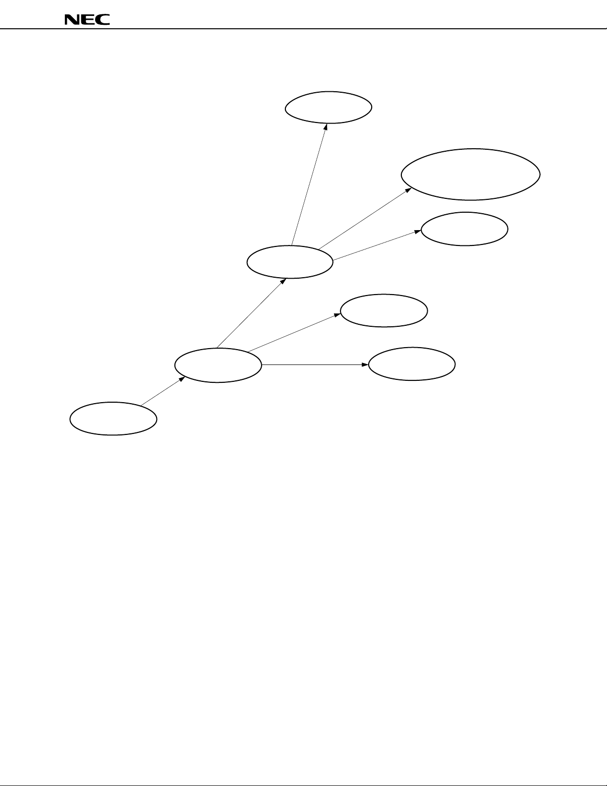
78K/III Series Product Development
PD78372 subseries
µ
µ
PD78361A, 78362A
High-performance CPU,
sum-of-products instruction added
High-speed, multi-function,
reinforced interrupt,
10-bit A/D
Reinforced timer,
A/D added
µ
PD78352A subseries
Reinforced timer and
A/D, expanded ROM
and RAM
Pulse output function
µ
PD78322 subseries
(for control application in OA and FA fields)
for inverter control
(for control unit of automotive appliances)
Pulse output function
for inverter control,
expanded ROM, RAM
A/D, D/A relative instruction
added, expanded ROM, RAM
(for HDD)
µ
PD78334 subseries
(for control application in OA and FA fields)
µ
PD78328 subseries
PD78366A subseries
µ
PD78361A
µ
µ
PD78362A
µ
PD78P364A
µ
PD78356 subseries
(for inverter)
µ
PD78363A
PD78365A
µ
µ
PD78366A
µ
PD78368A
µ
PD78P368A
(for inverter)
(for camera, HDD)
PD78312A subseries
µ
(for control application in OA and FA fields)
2
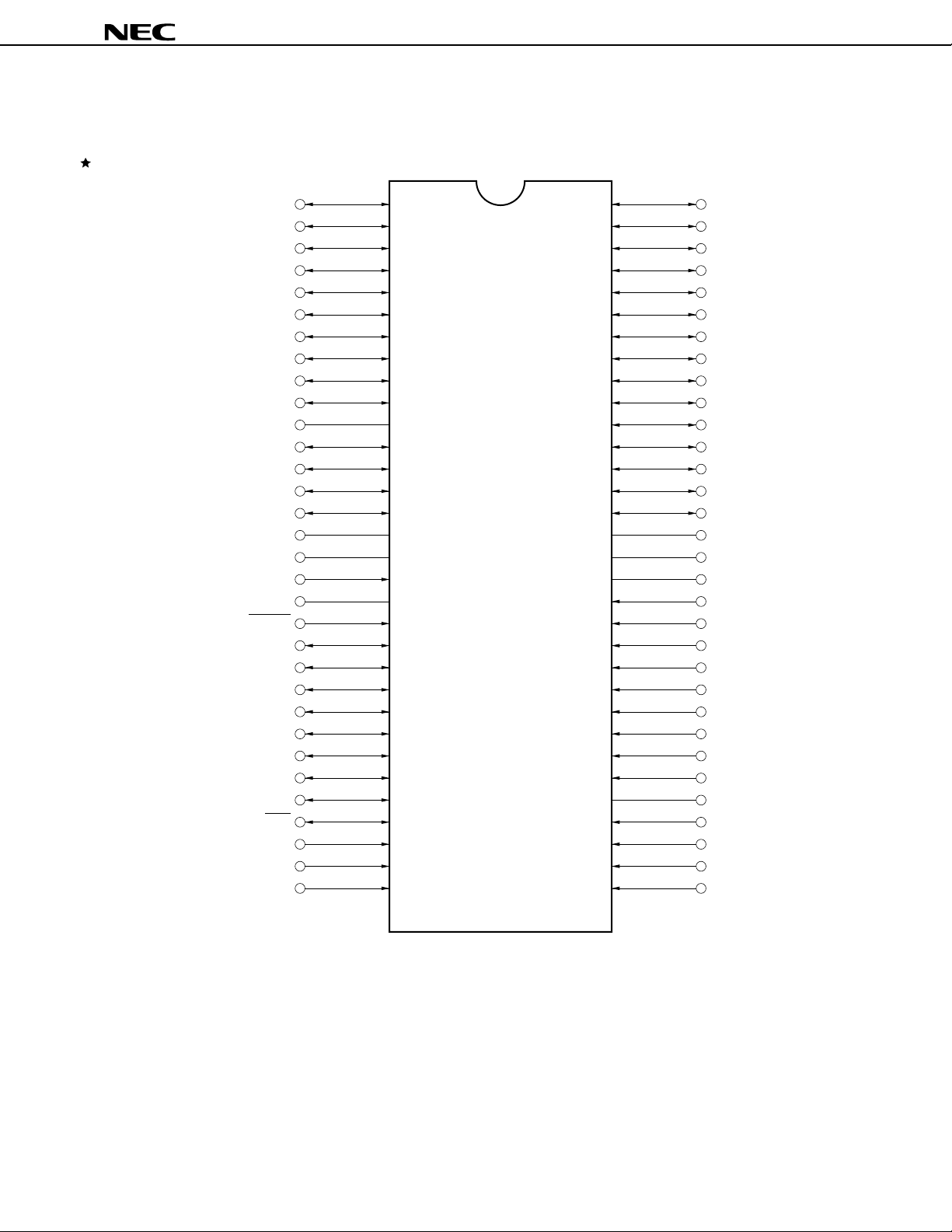
PIN CONFIGURATION (TOP VIEW)
• 64-pin plastic shrink DIP (750 mil)
µ
PD78361ACW-×××, 78362ACW-×××
µ
PD78361A, 78362A
P57
P90
P91
P92
P80/TO00
P81/TO01
P82/TO02
P83/TO03
P84/TO04
P85/TO05
VSS
P00/RTP0
P01/RTP1
P02/RTP2
P03/RTP3
VDD
VSS
X1
X2
RESET
P04/PWM0
P05/PWM1/TCUD
P06/TO40/TIUD
P07/TCLRUD
P30/TxD
P31/RxD
P32/SO/SB0
P33/SI/SB1
P34/SCK
MODE
P20/NMI
P21/INTP0
1
2
3
4
5
6
7
8
9
10
11
12
13
14
15
16
17
18
19
20
21
22
23
24
25
26
27
28
29
30
31
32
64
63
62
61
60
59
58
57
56
55
54
53
52
51
50
49
48
47
46
45
44
43
42
41
40
39
38
37
36
35
34
33
P56
P55
P54
P53
P52
P51
P50
P47
P46
P45
P44
P43
P42
P41
P40
VSS
VDD
AVDD
AVREF
P77/ANI7
P76/ANI6
P75/ANI5
P74/ANI4
P73/ANI3
P72/ANI2
P71/ANI1
P70/ANI0
AVSS
P25/INTP4
P24/INTP3/TI
P23/INTP2
P22/INTP1
Remark ××× indicates a ROM code suffix.
3

µ
PD78361A, 78362A
P00-P07 : Port0
P20-P25 : Port2
P30-P34 : Port3
P40-P47 : Port4
P50-P57 : Port5
P70-P77 : Port7
P80-P85 : Port8
P90-P92 : Port9
RTP0-RTP3 : Real-time Port
NMI : Nonmaskable Interrupt
INTP0-INTP4 : Interrupt From Peripherals
TO00-TO05, TO40 : Timer Output
TI : Timer Input
TIUD : Timer Input Up Down Counter
TCUD : Timer Control Up Down Counter
TCLRUD : Timer Clear Up Down Counter
ANI0-ANI7 : Analog Input
XD : Transmit Data
T
XD : Receive Data
R
SI : Serial Input
SO : Serial Output
SB0, SB1 : Serial Bus
SCK : Serial Clock
PWM0, PWM1 : Pulse Width Modulation Output
MODE : Mode
RESET : Reset
X1, X2 : Crystal
DD : Analog VDD
AV
AVSS : Analog VSS
AVREF : Analog Reference Voltage
DD : Power Supply
V
VSS : Ground
4
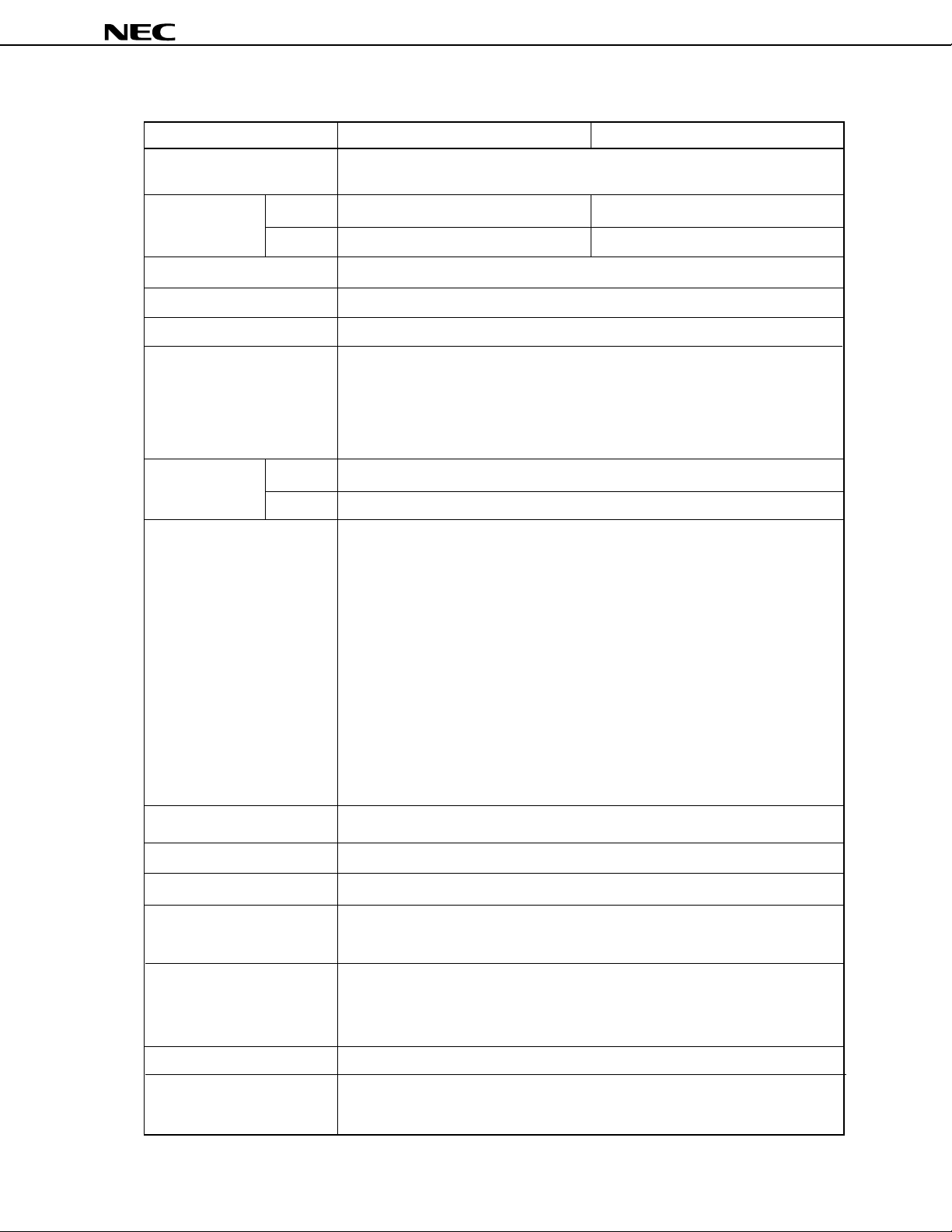
FUNCTIONAL OUTLINE
µ
PD78361A, 78362A
Item
Minimum instruction execution
time
Internal memory ROM
RAM
Memory space
General-purpose registers
Number of basic instructions
Instruction set
I/O lines Input
I/O
Real-time pulse unit
µ
PD78361A
125 ns (internal clock: 16 MHz, external clock: 8 MHz)
32K bytes 24K bytes
2K bytes 768 bytes
64K bytes
8 bits × 16 × 8 banks
115
• 16-bit transfer/operation
• Multiplication/division (16 bits × 16 bits, 32 bits ÷ 16 bits)
• Bit manipulation
• String
• Sum-of-products operation (16 bits × 16 bits + 32 bits)
• Relative operation
14 (of which 8 are shared with analog input)
38
• 16-bit timer × 1
10-bit dead time timer × 3
16-bit compare register × 4
2 kinds of output mode can be selected
Mode 0, set-reset output: 6 channels
Mode 1, buffer output: 6 channels
• 16-bit timer × 1
16-bit compare register × 1
• 16-bit timer × 1
16-bit capture register × 1
16-bit capture/compare register × 1
• 16-bit timer × 1
16-bit capture register × 2
16-bit capture/compare register × 1
• 16-bit timer × 1
16-bit compare register × 2
16-bit resolution PWM output: 1 channel
µ
PD78362A
Real-time output port
PWM unit
A/D converter
Serial interface
Interrupt function
Package
Others
Pulse outputs associated with real-time pulse unit: 4 lines
8-/9-/10-/12-bit resolution variable PWM output: 2 channels
10-bit resolution, 8 channels
Dedicated baud rate generator
UART: 1 channel
Clocked serial interface/SBI: 1 channel
• External: 6, internal: 14 (of which 2 are multiplexed with external)
• 4 priority levels can be specified through software
• 3 types of interrupt service modes selectable
(vectored interrupt, macro service, and context switching)
64-pin plastic shrink DIP (750 mil)
• Watchdog timer
• Standby function (HALT and STOP modes)
• PLL control circuit
5

DIFFERENCES BETWEEN µPD78362A AND µPD78366A
µ
PD78361A, 78362A
Item
Internal ROM
I/O lines
Serial Interface
External expansion function
ROM-less mode
MODE setting
Package
Product name
ROM
RAM
Input
I/O
µ
PD78362A
24K bytes 32K bytes
786 bytes 2K bytes
14 (of which 8 are multiplexed with analog input)
38
Dedicated baud rate generator
UART: 1 channel
Clocked serial interface/SBI: 1 channel
None
None
Always set as follows:
MODE = L
64-pin plastic shrink DIP (750 mil)
49
Dedicated baud rate generator
UART (with pin selection function):
1 channel
Clocked serial interface/SBI:
1 channel
Provided
Provided
• In ordinary operation mode:
MODE0, 1 = LL
• In ROM-less mode:
MODE0, 1 = HH
80-pin plastic QFP (14 × 20 mm)
µ
PD78366A
6
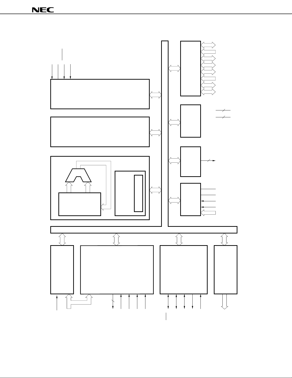
BLOCK DIAGRAM
X1
X2
RESET
MODE
SYSTEM
CONTROL
&
&
BUS
CONTROL
CONTROL
PREFETCH
µ
PD78361A, 78362A
8
P0
6
P2
5
P3
8
P4
8
PORT
P5
8
P6
6
P7
3
P8
2
3
DD
V
V
SS
ROM/RAM BCU
EXU
GENERAL
Main RAM
ROM
24K × 8
32K × 8
ALU
&
DATA
128 × 8
REGISTERS
&
128 × 8
MEMORY
RAM
512 × 8
Peripheral
1792 × 8
MICRO
SEQUENCE
CONTROL
MICRO ROM
WATCHDOG
TIMER
2
RWM
A/D
CONVERTER
8
PWM
DD
AV
AV
SS
AV
REF
INTP2
ANI
INTERRUPT
CONTROLLER
PROGRAMMABLE
5
5
NMI
INTP
UNIT
(REAL-TIME
PULSE UNIT)
TIMER/COUNTER
4
7
TI
TO
TIUD
TCUD
TCLRUD
SCK
(SBI)
SERIAL
INTERFACE
SI/B1
SO/SB0
(UART)
TxD
RxD
REAL-TIME
OUTPUT PORT
4
RTP
Remark Internal ROM and RAM capacities differ depending on the product.
7

µ
PD78361A, 78362A
TABLE OF CONTENTS
1. PIN FUNCTIONS ...................................................................................................................... 10
1.1 PORT PINS ..................................................................................................................................... 10
1.2 PINS OTHER THAN PORT PINS .................................................................................................. 11
1.3 PIN I/O CIRCUITS AND PROCESSING OF UNUSED PINS....................................................... 12
2. CPU ARCHITECTURE ............................................................................................................. 14
2.1 MEMORY SPACE........................................................................................................................... 14
2.2 DATA MEMORY ADDRESSING .................................................................................................... 16
2.3 PROCESSOR REGISTERS ........................................................................................................... 18
2.3.1 Control Registers................................................................................................................. 18
2.3.2 General-Purpose Registers..................................................................................................19
2.3.3 Special Function Registers (SFR) ........................................................................................20
3. FUNCTIONAL BLOCKS........................................................................................................... 26
3.1 EXECUTION UNIT (EXU)............................................................................................................... 2 6
3.2 BUS CONTROL UNIT (BCU)......................................................................................................... 2 6
3.3 ROM/RAM ....................................................................................................................................... 26
3.4 PORT FUNCTIONS ........................................................................................................................ 2 6
3.5 CLOCK GENERATOR CIRCUIT ................................................................................................... 28
3.6 REAL-TIME PULSE UNIT (RPU) .................................................................................................. 30
3.7 REAL-TIME OUTPUT PORT (RTP) .............................................................................................. 37
3.8 A/D CONVERTER .......................................................................................................................... 38
3.9 SERIAL INTERFACE ..................................................................................................................... 39
3.10 PWM UNIT ...................................................................................................................................... 41
3.11 WATCHDOG TIMER (WDT) .......................................................................................................... 42
4. INTERRUPT FUNCTIONS ....................................................................................................... 43
4.1 OUTLINE ......................................................................................................................................... 43
4.2 MACRO SERVICE.......................................................................................................................... 44
4.3 CONTEXT SWITCHING ................................................................................................................. 47
4.3.1 Context Switching Function by Interrupt Request ................................................................47
4.3.2 Context Switching Function by BRKCS Instruction ..............................................................48
4.3.3 Restoration from Context Switching .....................................................................................48
5. STANDBY FUNCTIONS ...................................................................................................................... 4 9
6. RESET FUNCTION ................................................................................................................... 50
7. INSTRUCTION SET .................................................................................................................. 51
8. EXAMPLE OF SYSTEM CONFIGURATION ........................................................................... 65
9. ELECTRICAL SPECIFICATIONS ............................................................................................ 66
10. PACKAGE DRAWING.............................................................................................................. 75
8

µ
PD78361A, 78362A
11. RECOMMENDED SOLDERING CONDITIONS ...................................................................... 76
APPENDIX A. DIFFERENCES BETWEEN µPD78362A AND µPD78328.................................. 77
APPENDIX B. TOOLS.................................................................................................................... 78
B.1 DEVELOPMENT TOOLS ............................................................................................................... 78
B.2 EMBEDDED SOFTWARE.............................................................................................................. 83
9

µ
PD78361A, 78362A
1. PIN FUNCTIONS
1.1 PORT PINS
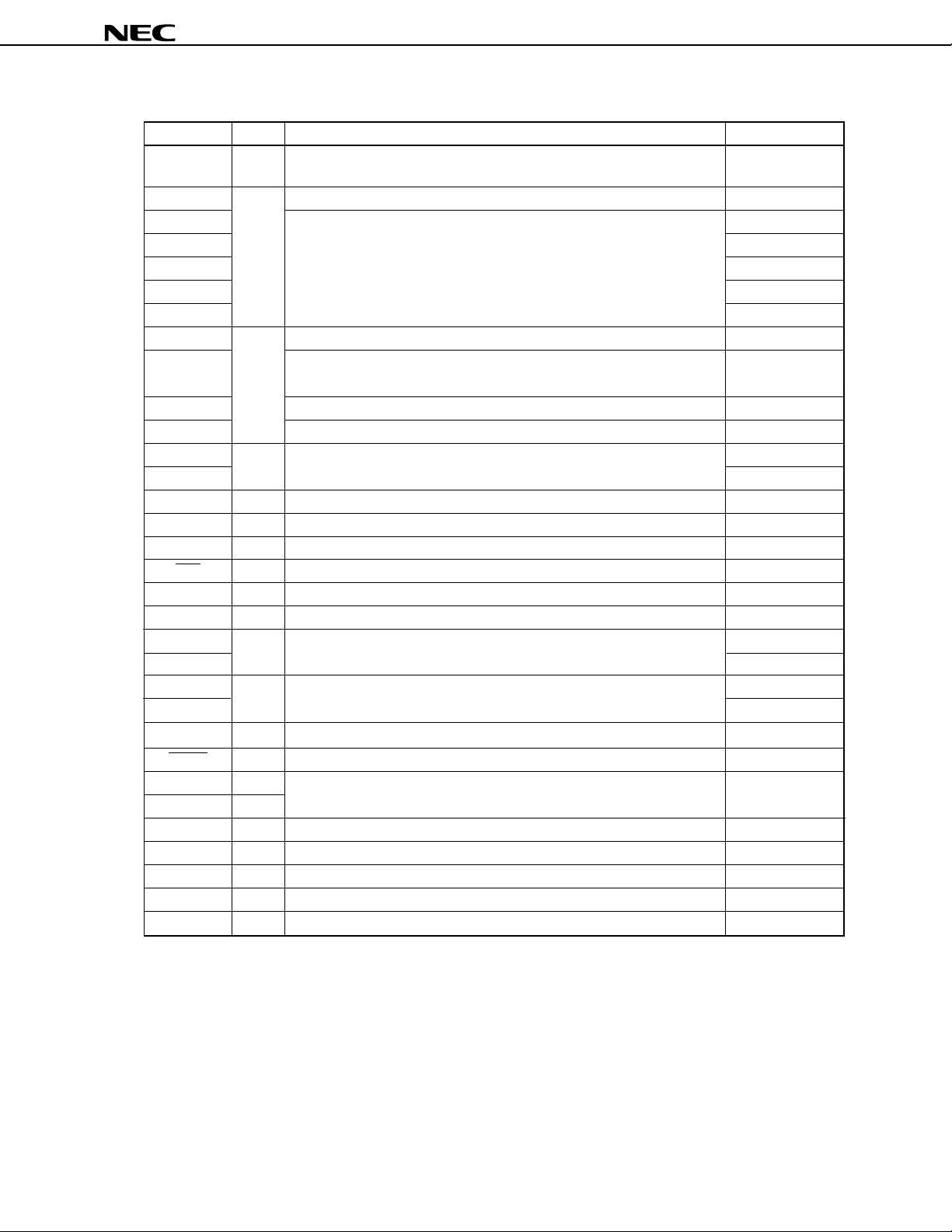
Pin name I/O Function Shared by:
P00-P03
P04
P05
P06
P07
P20
P21
P22
P23
P24
P25
P30
P31
P32
P33
P34
Input
Port 0.
8-bit I/O port.
Can be set in input or output mode in 1-bit units.
I/O
Port 2.
6-bit input port.
Port 3.
5-bit I/O port.
Can be set in input or output mode in 1-bit units.
I/O
RTP0-RTP3
PWM0
TCUD/PWM1
TIUD/TO40
TCLRUD
INTP0
INTP1
INTP2
INTP3/TI
INTP4
SO/SB0
SI/SB1
NMI
TXD
RXD
SCK
P40-P47
P50-P57
P70-P77
P80-P85
P90-P92
I/O
I/O
Input
I/O
I/O
Port 4.
8-bit I/O Port.
Can be set in input or output mode in 8-bit units.
Port 5.
8-bit I/O port.
Can be set in input or output mode in 1-bit units.
Port 7.
8-bit input port
Port 8.
6-bit I/O port.
Can be set in input or output mode in 1-bit units.
Port 9.
3-bit I/O port.
Can be set in input or output mode in 1-bit units.
–
–
ANI0-ANI7
TO00-TO05
–
10
µ
PD78361A, 78362A
1.2 PINS OTHER THAN PORT PINS
Pin name I/O Function Shared by:
RTP0-RTP3
NMI
INTP0
INTP1
INTP2
INTP3
INTP4
TI
TCUD
TIUD
TCLRUD
TO00-TO05
TO40
ANI0-ANI7
TXD
RXD
SCK
SI
SO
SB0
SB1
PWM0
PWM1
MODE
RESET
X1
X2
AVREF
AVDD
AVSS
VDD
VSS
Output
Input
Input
Output
Input
Output
Input
I/O
Input
Ouput
I/O
Output
Input
Input
Input
–
Input
–
–
–
–
Real-time output port that outputs pulses in synchronization with trigger
signal from real-time pulse unit.
Non-maskable interrupt request input.
External interrupt request input.
External count clock input to timer 1.
Count operation selection control signal input to up/down counter (timer
4).
External count clock input to up/down counter (timer 4).
Clear signal input to up/down counter (timer 4).
Pulse output from real-time pulse unit.
Analog input to A/D converter.
Serial data output of asynchronous serial interface.
Serial data input of asynchronous serial interface.
Serial clock input/output of clocked serial interface.
Serial data input of clocked serial interface in 3-line mode.
Serial data output of clocked serial interface in 3-line mode.
Serial data input/output of clocked serial interface in SBI mode.
PWM signal output.
Control signal input to set operation mode. Connected to VSS.
System reset input
Crystal oscillator connecting pins for system clock. If a clock is externally
supplied, input it to pin X1. Leave pin X2 open.
A/D converter reference voltage input.
A/D converter analog power supply.
A/D converter GND.
Positive power supply
GND
P00-P03
P24/TI
P24/INTP3
P05/PWM1
P06/TO40
P80-P85
P06/TIUD
P70-P77
P33/SB1
P32/SB0
P32/SO
P33/SI
P05/TCUD
P20
P21
P22
P23
P25
P07
P30
P31
P34
P04
–
–
–
–
–
–
–
–
11

µ
PD78361A, 78362A
1.3 PIN I/O CIRCUITS AND PROCESSING OF UNUSED PINS
Table 1-1 shows the I/O circuit types of the respective pins, and recommended connections of the unused
pins. Figure 1-1 shows the circuits of the respective pins.
Table 1-1. Pin I/O Circuit Type and Recommended Connections of Unused Pins
Pin I/O circuit type Recommended connections
P00/RTP0-P03/RTP3
P04/PWM0
P05/TCUD/PWM1
P06/TIUD/TO40
P07/TCLRUD
P20/NMI
P21/INTP0
P22/INTP1
P23/INTP2
P24/INTP3/TI
P25/INTP4
P30/TXD
P31/RXD
P32/SO/SB0
P33/SI/SB1
P34/SCK
P40-P47
P50-P57
P70/ANI0-P77/ANI7
P80/TO00-P85/TO05
P90-P92
MODE
RESET
AVREF, AVSS
AVDD
5-A
2
2-A
5-A
8-A
5-A
9
5-A
1
2
–
Input : Independently connect to VDD or VSS through resistor
Output : Open
Connect to VSS
Input : Independently connect to VDD or VSS through resistor
Output : Open
Connect to VSS
Input : Independently connect to VDD or VSS through resistor
Output : Open
–
Connect to VSS
Connect to VDD
12
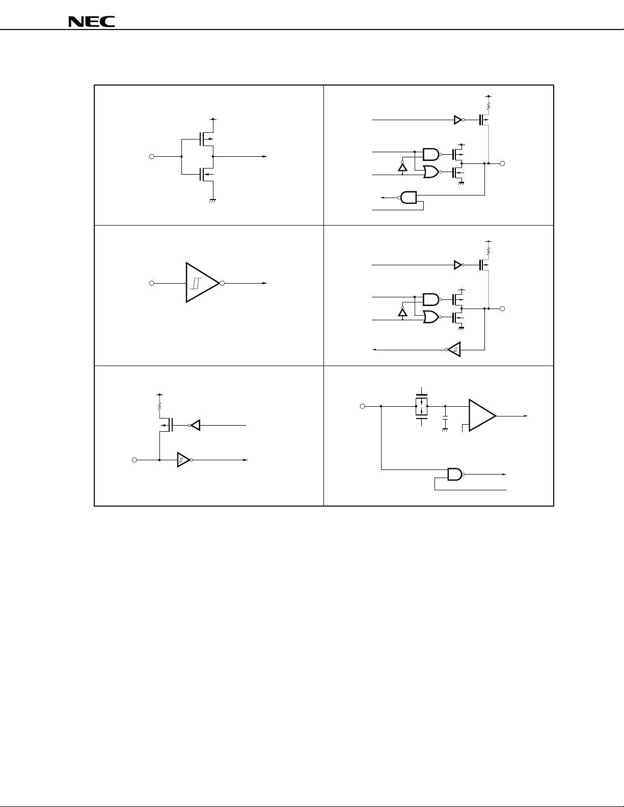
Figure 1-1. Pin I/O Circuits
µ
PD78361A, 78362A
Type 1 Type 5-A
V
DD
pull-up
enable
P-ch
IN
N-ch
data
output
disable
input
enable
Type 2 Type 8-A
pull-up
IN
Schmitt trigger input with hysteresis characteristics
Type 2-A
DD
V
P-ch
IN
pull-up
enable
enable
data
output
disable
Type 9
IN
P-ch
N-ch
P-ch
V
DD
P-ch
N-ch
P-ch
V
DD
P-ch
N-ch
Comparator
+
–
ref
V
(Threshold voltage)
DD
V
V
DD
IN/OUT
IN/OUT
Schmitt trigger input with hysteresis characteristics
input
enable
13
µ
PD78361A, 78362A
2. CPU ARCHITECTURE
2.1 MEMORY SPACE
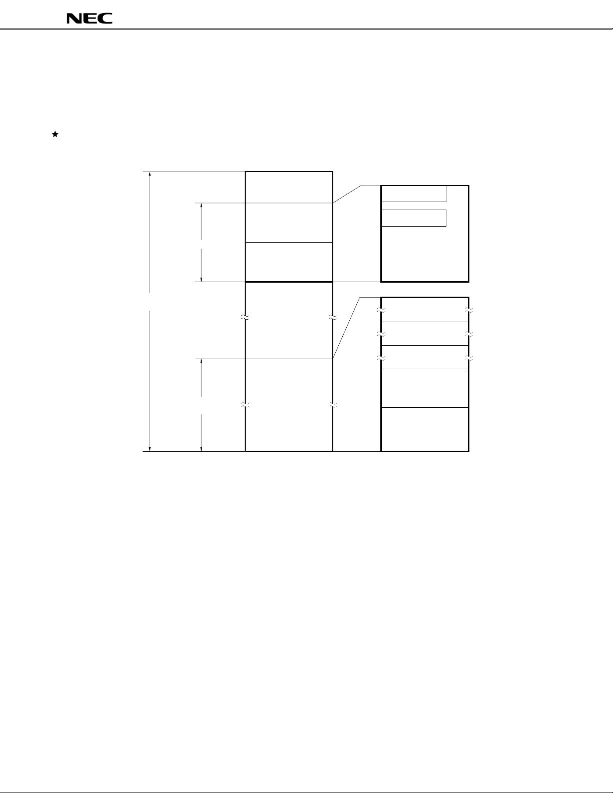
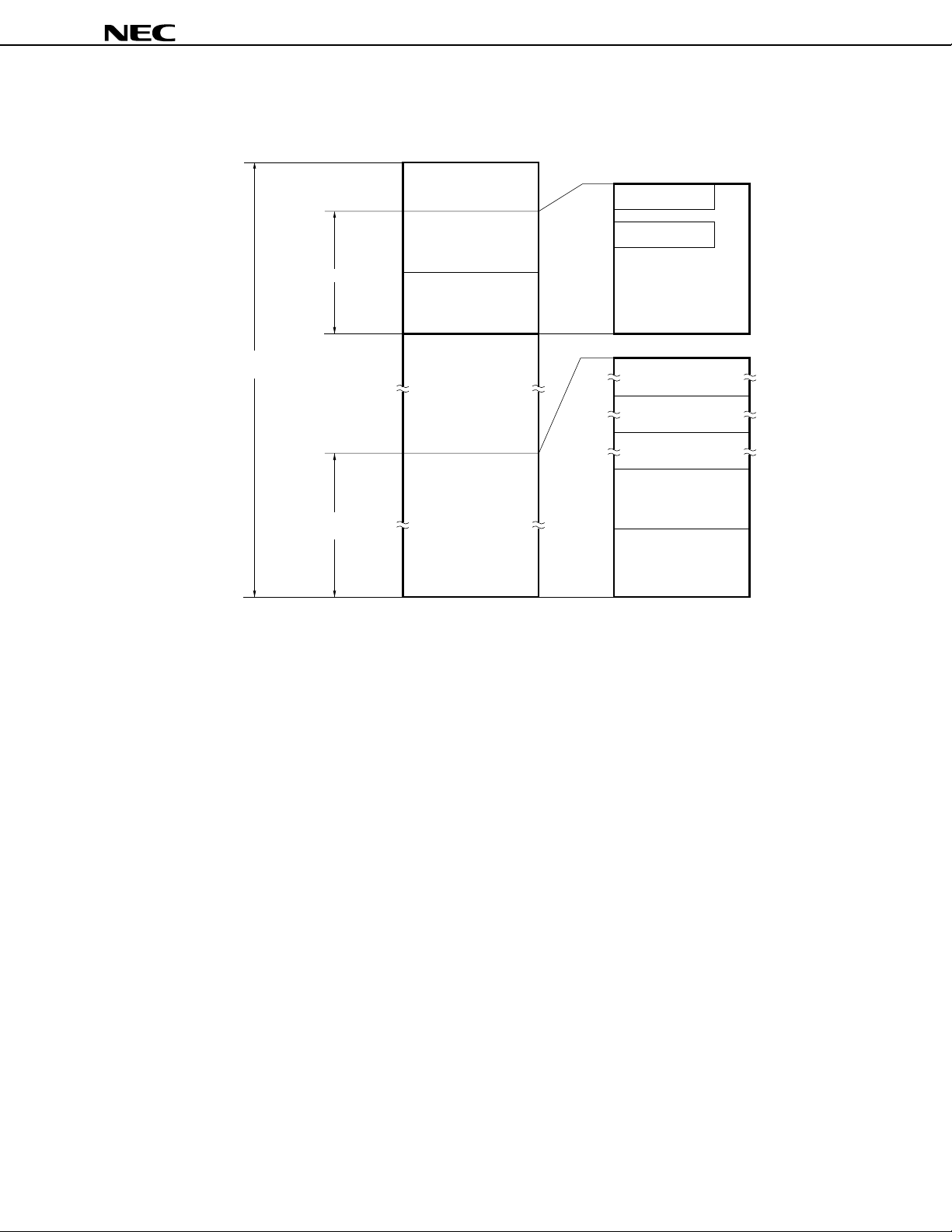
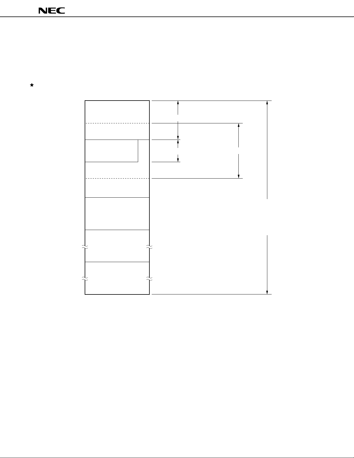
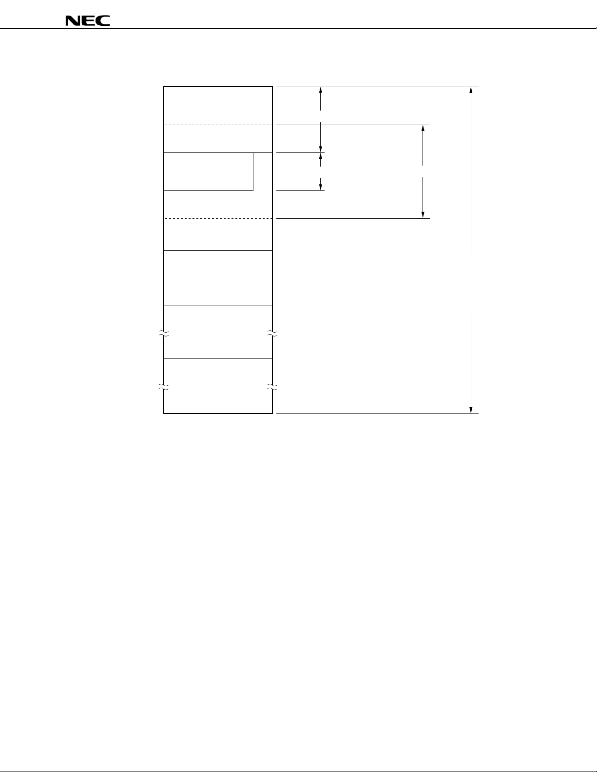
The µPD78362A can access a memory space of 64K bytes. Figure 2-1 and 2-2 show the memory map.
Figure 2-1. Memory Map (µPD78361A)
MODE = L
Memory space
×
8)
(64 K
Data memory
Program memory
Data memory
FFFFH
FF00H
FEFFH
FF00H
FDFFH
F700H
F6FFH
8000H
7FFFH
0000H
Special function register
(SFR)
(256 × 8)
Main RAM
(256 × 8)
Peripheral RAM
(1792 × 8)
Cannot be used
Internal ROM
(32768 × 8)
FEFFH
FE80H
FE25H
FE06H
7FFFH
0FFFH
07FFH
General-purpose
register (128 × 8)
Macro service
control (32 × 8)
F700H
1000H
0800H
0080H
007FH
0040H
003FH
0000H
Program area
CALLF instruction entry area
Program area
CALLT instruction table area
Vector table area
Data area
(768 × 8)
(2048 × 8)
(64 × 8)
(64 × 8)
Caution For word access (including stack operations) to the main RAM area (FE00H-FEFFH), the
address that specifies the operand must be an even value.
14
Memory space
×
8)
(64 K
Figure 2-2. Memory Map (µPD78362A)
Data memory
Program memory
Data memory
FFFFH
FF00H
FEFFH
FF00H
FDFFH
FC00H
FBFFH
6000H
5FFFH
0000H
MODE = L
Special function register
(SFR)
(256 × 8)
Main RAM
(256 × 8)
Peripheral RAM
(512 × 8)
Cannot be used
Internal ROM
(24576 × 8)
µ
PD78361A, 78362A
FEFFH
FE80H
FE25H
FE06H
FC00H
5FFFH
1000H
0FFFH
0800H
07FFH
0080H
007FH
0040H
003FH
0000H
General-purpose
register (128 × 8)
Macro service
control (32 × 8)
Program area
CALLF instruction entry area
Program area
CALLT instruction table area
Vector table area
Data area
(768 × 8)
(2048 × 8)
(64 × 8)
(64 × 8)
Caution For word access (including stack operations) to the main RAM area (FE00H-FEFFH), the
address that specifies the operand must be an even value.
15
µ
PD78361A, 78362A
2.2 DATA MEMORY ADDRESSING
The µPD78362A is provided with many addressing modes that improve the operability of the memory and
can be used with high-level languages. Especially, an area of addresses FC00H-FFFFH (F700H-FFFFH
µ
PD78361A) to which the data memory is mapped can be addressed in a mode peculiar to the functions
in the
provided in this area, including special function registers (SFR) and general-purpose registers.
Figure 2-3. Data Memory Addressing (µPD78361A)
FFFFH
FF20H
FF1FH
FF00H
FEFFH
FE80H
FE7FH
FE20H
FE1FH
FE00H
FDFFH
F700H
F6FFH
8000H
7FFFH
Special function
register
(SFR)
General-purpose
register
Main RAM
Peripheral RAM
Cannot be used
SFR addressing
Register addressing
Short direct addressing
Direct addressing
Register indirect addressing
Based addressing
Based indexed addressing
Based indexed addressing
(with displacement)
Internal ROM
0000H
Caution For word access (including stack oprations) to the main RAM area (FE00H-FEFFH), the
address that specifies the operand must be an even value.
16
µ
PD78361A, 78362A
Figure 2-4. Data Memory Addressing (µPD78362A)
FFFFH
FF20H
FF1FH
FF00H
FEFFH
FE80H
FE7FH
FE20H
FE1FH
FE00H
FDFFH
FC00H
FBFFH
6000H
5FFFH
Special function
register
(SFR)
General-purpose
register
Main RAM
Peripheral RAM
Cannot be used
SFR addressing
Register addressing
Short direct addressing
Direct addressing
Register indirect addressing
Based addressing
Based indexed addressing
Based indexed addressing
(with displacement)
Internal ROM
0000H
Caution For word access (including stack oprations) to the main RAM area (FE00H-FEFFH), the
address that specifies the operand must be an even value.
17
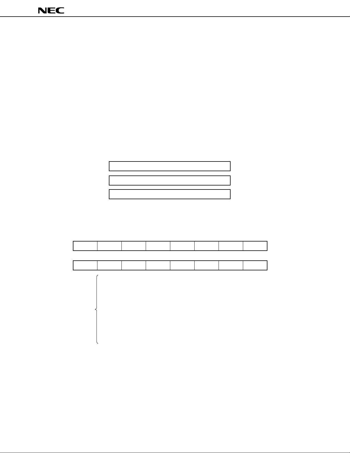
2.3 PROCESSOR REGISTERS
The µPD78362A is provided with the following three types of processor registers:
• Control registers
• General-purpose registers
• Special function registers (SFRs)
2.3.1 Control Registers
(1) Program counter (PC)
This is a 16-bit register that holds an address of the instruction to be executed next.
(2) Program status word (PSW)
This 16-bit register indicates the status of the CPU as a result of instruction execution.
(3) Stack pointer (SP)
This 16-bit register indicates the first address of the stack area (LIFO) of the memory.
Figure 2-5. Configuration of Control Registers
15 0
PC
µ
PD78361A, 78362A
PSW
PSW
SP
Figure 2-6. Configuration of PSW
15
UF RBS2 RBS1 RBS0 0 0 0 0
7
S Z RSS AC IE P/V 0 CY
UF : User flag
RBS0-RBS2: Register bank select flag
S : Sign flag (MSB of execution result)
Z : Zero flag
RSS : Register set select flag
AC : Auxiliary carry flag
IE : Interrupt request enable flag
P/V : Parity/overflow flag
CY : Carry flag
8
0
18
µ
15 0
RP0
RP1
RP2
RP3
RP4
RP5
RP6
RP7
Bank 7
Bank 1
Bank 0
PD78361A, 78362A
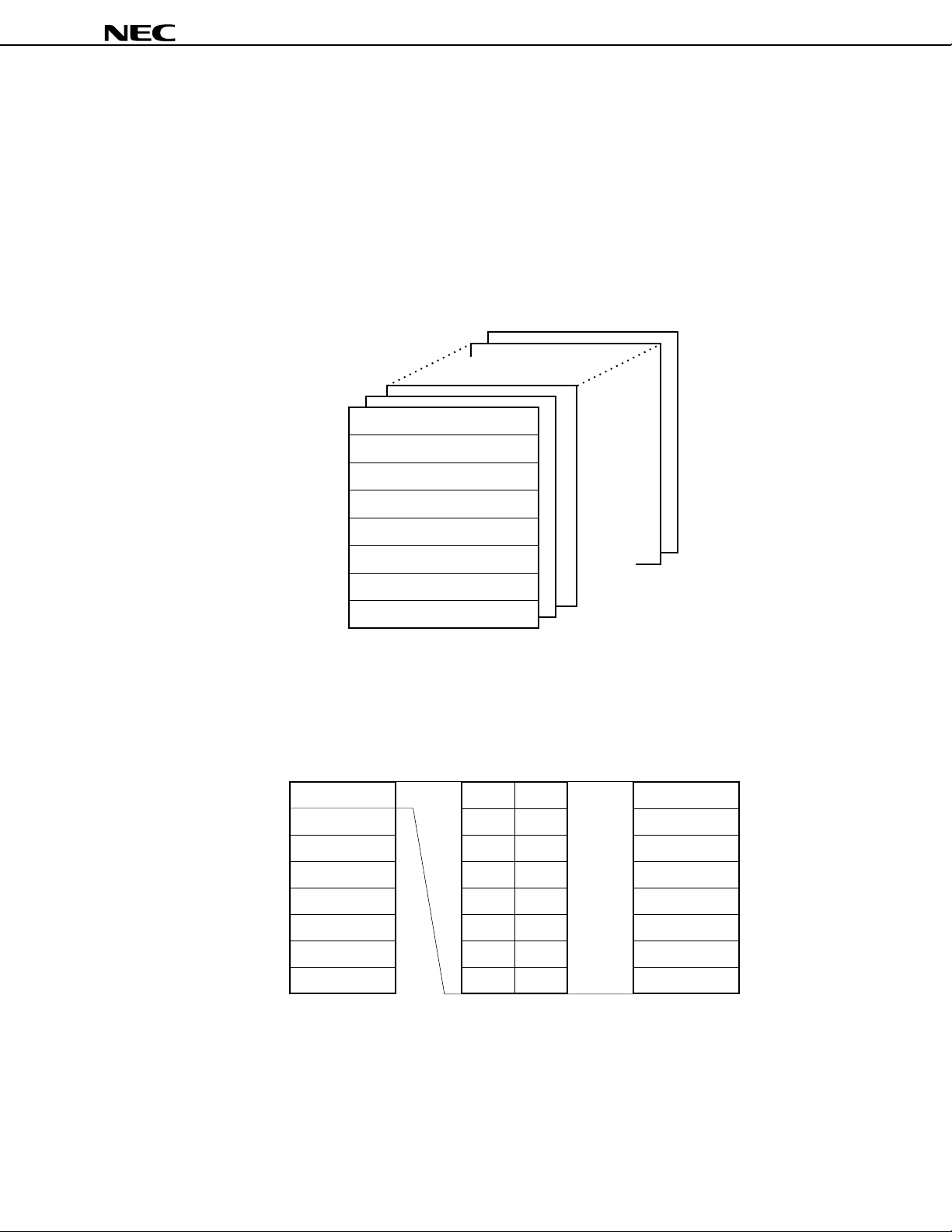
2.3.2 General-Purpose Registers
The µPD78362A is provided with eight banks of general-purpose registers with one bank consisting of 8
words × 16 bits. Figure 2-7 shows the configuration of the general-purpose register banks. The general-purpose
registers are mapped to an area of addresses FE80H-FEFFH. Each of these registers can be used as an 8bit register. In addition, two registers can be used as one 16-bit register pair (refer to Figure 2-8 ). These
general-purpose registers facilitate complicated multitask processing.
Figure 2-7. Configuration of General-Purpose Register Banks
Figure 2-8. Processing Bits of General-Purpose Registers
FEFFH
FE80H
RBNK0
RBNK1
RBNK2
RBNK3
RBNK4
RBNK5
RBNK6
RBNK7
8-bit processing 16-bit processing
R15
R13
R11
R9
R7
R5
R3
R1
R14
R12
R10
R8
R6
R4
R2
R0
(FH)
(DH)
(BH)
(9H)
(7H)
(5H)
(3H)
(1H)
7 07 0 15 0
RP7
RP6
RP5
RP4
RP3
RP2
RP1
RP0
(EH)
(CH)
(AH)
(8H)
(6H)
(4H)
(2H)
(0H)
19

µ
PD78361A, 78362A
2.3.3 Special Function Registers (SFR)
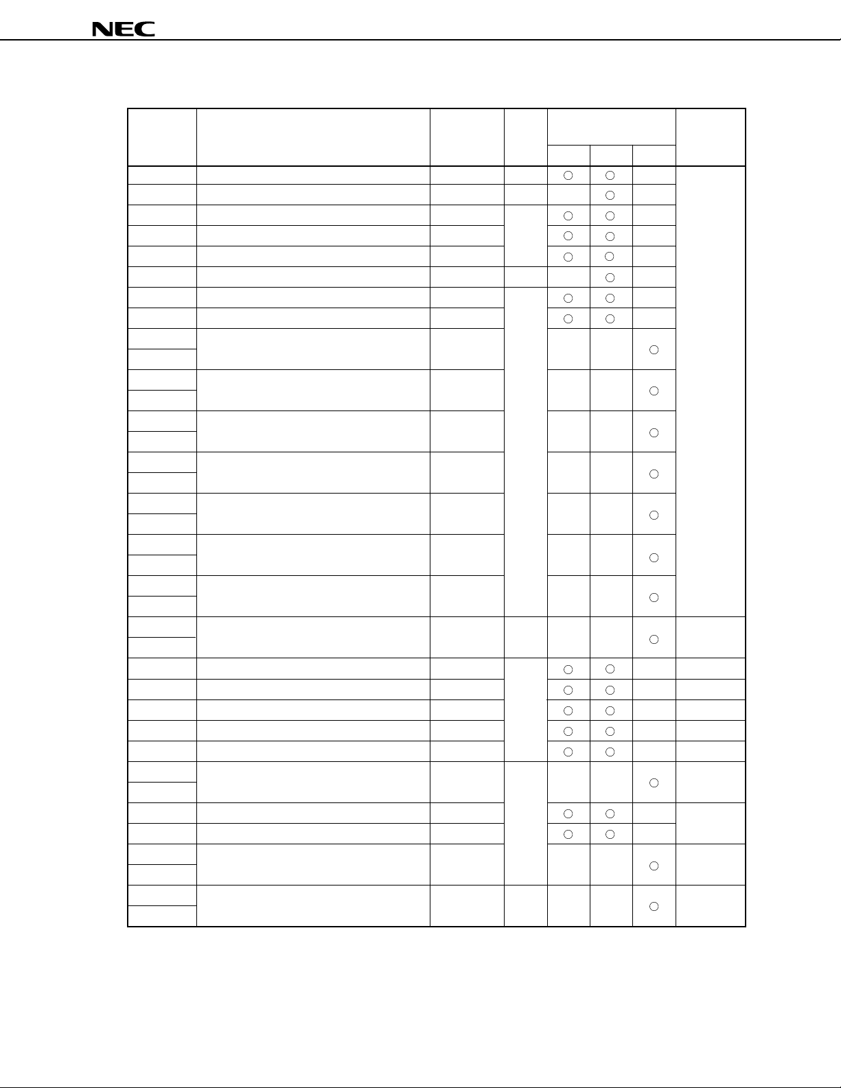
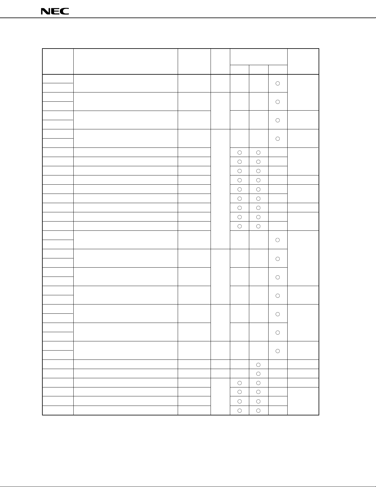
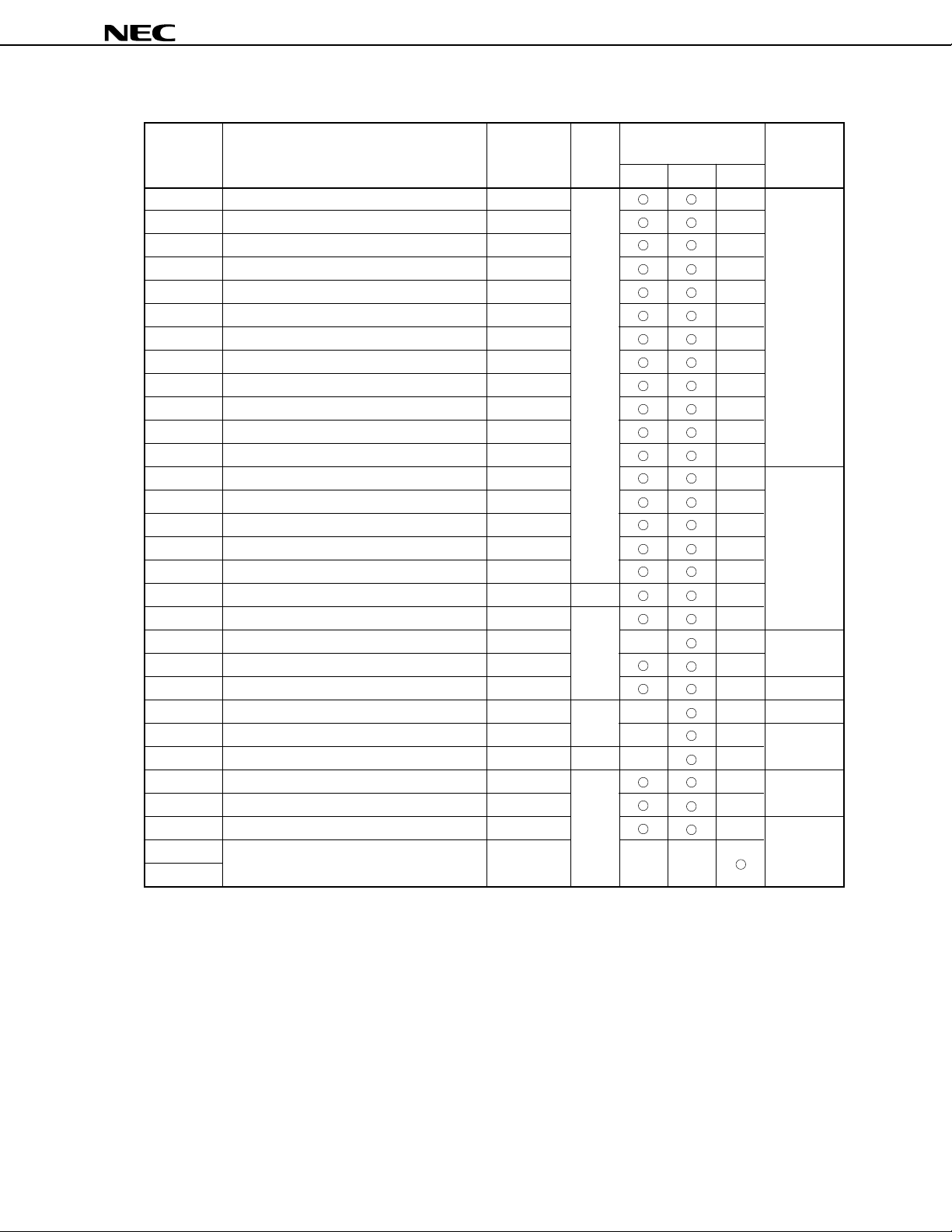
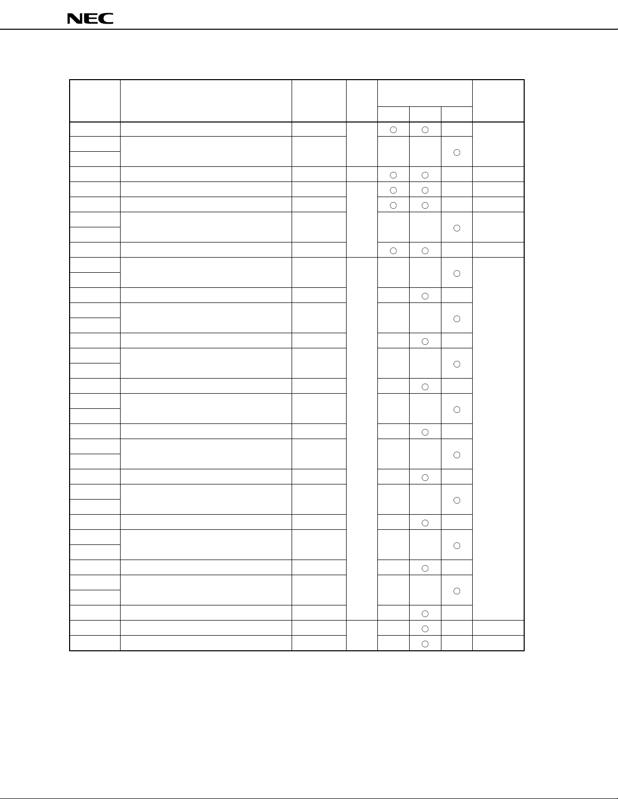
Special function registers (SFRs) are registers assigned special functions such as mode registers and control
registers for internal peripheral hardware, and are mapped to a 256-byte address space at FF00H through
FFFFH.
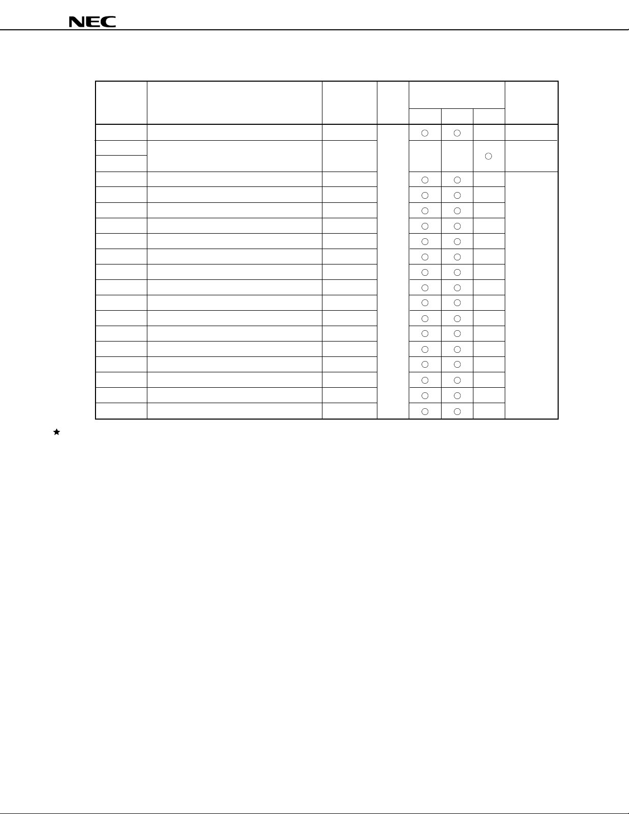
Table 2-1 lists the SFRs. The meanings of the symbols in this table are as follows:
• Symbol ................................... Indicates the mnemonic symbol for an SFR.
This mnemonic can be coded in the operand field of an instruction.
• R/ W ........................................ Indicates whether the SFR can be read or written.
R/W : Read/write
R : Read only
W : Write only
• Bit units for manipulation ...... Indicates bit units in which the SFR can be manipulated. The SFRs that
can be manipulated in 16-bit units can be coded as an sfrp operand.
Specify an even address for these SFRs.
The SFRs that can be manipulated in 1-bit units can be coded as the
operand of bit manipulation instructions.
• On reset ................................. Indicates the status of the register at RESET input.
Cautions1. Do not access the addresses in the range FF00H-FFFFH to which no special function
register is allocated. If these addresses are accessed, malfunctio ning may occur.
2. Do not write data to the read-only registers. Otherwise, the internal circuit may not
operate normally.
3. When using read data as byte data, process undefined bit(s) first.
4. TOUT and TXS are write-only registers. Do no read these registers.
5. Bits 0, 1, and 4 of SBIC are write-only bits. When these bits are read, they are always
"0".
20
FF00H
FF02H
FF03H
FF04H
FF05H
FF07H
FF08H
FF09H
FF10H
FF11H
FF12H
FF13H
FF14H
FF15H
FF16H
FF17H
FF18H
FF19H
FF1AH
FF1BH
FF1CH
FF1DH
FF1EH
FF1FH
FF20H
FF23H
FF25H
FF28H
FF29H
FF2CH
FF2DH
FF2EH
FF2FH
FF30H
FF31H
FF32H
FF33H
Table 2-1. List of Special Function Registers (1/5)
Port 0
Port 2
Port 3
Port 4
Port 5
Port 7
Port 8
Port 9
Compare register 00
Compare register 01
Compare register 02
Compare register 03
Buffer register CM00
Buffer register CM01
Buffer register CM02
Timer register 0
Port 0 mode register
Port 3 mode register
Port 5 mode register
Port 8 mode register
Port 9 mode register
Reload register
Timer unit mode register 0
Timer unit mode register 1
Compare register 10
Timer register 1
P0
P2
P3
P4
P5
P7
P8
P9
CM00
CM01
CM02
CM03
BFCM00
BFCM01
BFCM02
TM0
PM0
PM3
PM5
PM8
PM9
DTIME
TUM0
TUM1
CM10
TM1
R/W
R
R/W
R
R/W
R
R/W
R/W
R
µ
PD78361A, 78362A
Bit units for
manipulation
1 bit 8 bits 16 bits
––
––
––
––
––
––
––
––
––
––
––
––
––
On resetAddress Special function register (SFR) Symbol R/W
–
–
–
–
–
–
Undefined
0000H
–
–
–
–
–
–
–
FFH
×××1 1111B
FFH
××11 1111B
×××× ×111B
Undefined
00H
Undefined
0000H
21
FF34H
FF35H
FF36H
FF37H
FF38H
FF39H
FF3AH
FF3BH
FF3CH
FF3DH
FF40H
FF43H
FF44H
FF45H
FF48H
FF4EH
FF4FH
FF50H
FF51H
FF52H
FF53H
FF54H
FF55H
FF56H
FF57H
FF58H
FF59H
FF5AH
FF5BH
FF5CH
FF5DH
FF5EH
FF5FH
FF60H
FF61H
FF62H
FF68H
Table 2-1. List of Special Function Registers (2/5)
Capture/compare register 20
Capture register 20
Timer register 2
Buffer register CM03
External interrupt mode register 0
External interrupt mode register 1
Port 0 mode control register
Port 3 mode control register
Pull-up resistor option register L
Pull-up resistor option register H
Port 8 mode control register
Sampling control register 0
Sampling control register 1
Capture/compare register 30
Capture register 30
Capture register 31
Timer register 3
Compare register 40
Compare register 41
Timer register 4
Timer control register 4
Timer out register
Real-time output port register
Real-time output port mode register
Port read control register
A/D converter mode register
CC20
CT20
TM2
BFCM03
INTM0
INTM1
PMC0
PMC3
PUOL
PUOH
PMC8
SMPC0
SMPC1
CC30
CT30
CT31
TM3
CM40
CM41
TM4
TMC4
TOUT
RTP
RTPM
PRDC
ADM
R/W
R
R/W
R
R/W
R
R/W
W
R/W
µ
PD78361A, 78362A
Bit units for
manipulation
1 bit 8 bits 16 bits
––
––
––
––
––
––
––
––
––
––
––
––
––
On resetAddress Special function register (SFR) Symbol R/W
Undefined
0000H
Underfined
–
–
–
–
–
–
–
–
–
–
–
–
–
00H
×××0 0000B
00H
××00 0000B
00H
Undefined
0000H
Undefined
0000H
00H
××01 0101B
Undefined
00H
22
FF70H
FF71H
FF72H
FF73H
FF74H
FF75H
FF76H
FF77H
FF78H
FF79H
FF7AH
FF7BH
FF7CH
FF7DH
FF7EH
FF7FH
FF80H
FF82H
FF84H
FF85H
FF86H
FF88H
FF8AH
FF8CH
FF8EH
FFA0H
FFA1H
FFA2H
FFA2H
FFA3H
Table 2-1. List of Special Function Registers (3/5)
Slave buffer register 0
Slave buffer register 1
Slave buffer register 2
Slave buffer register 3
Slave buffer register 4
Slave buffer register 5
Master buffer register 0
Master buffer register 1
Master buffer register 2
Master buffer register 3
Master buffer register 4
Master buffer register 5
Timer control register 0
Timer control register 1
Timer control register 2
Timer control register 3
Clocked serial interface mode register
Serial bus interface control register
Baud rate generator control register
Baud rate generator compare register
Serial I/O shift register
Asynchronous serial interface mode register
Asynchronous serial interface status register
Serial receive buffer: UART
Serial transfer shift register: UART
PWM control register 0
PWM control register 1
PWM register 0L
PWM register 0
SBUF0
SBUF1
SBUF2
SBUF3
SBUF4
SBUF5
MBUF0
MBUF1
MBUF2
MBUF3
MBUF4
MBUF5
TMC0
TMC1
TMC2
TMC3
CSIM
SBIC
BRGC
BRG
SIO
ASIM
ASIS
RXB
TXS
PWMC0
PWMC1
PWM0L
PWM0
R/W
R/W
R/W
R/W
µ
PD78361A, 78362A
Bit units for
manipulation
1 bit 8 bits 16 bits
Note
––
R
W
––
––
––
––
On resetAddress Special function register (SFR) Symbol R/W
–
–
–
–
–
–
Undefined
–
–
–
–
–
–
–
–
–
–
–
–
–
–
–
–
–
–
00H
Undefined
80H
00H
Undefined
00H
Undefined
Note Bits 7 and 5 : read/write
Bits 6, 3, and 2: read-only
Bits 4, 1, and 0: write-only
23
FFA4H
FFA4H
FFA5H
FFA8H
FFAAH
FFACH
FFACH
FFADH
FFADH
FFB0H
FFB1H
FFB1H
FFB2H
FFB3H
FFB3H
FFB4H
FFB5H
FFB5H
FFB6H
FFB7H
FFB7H
FFB8H
FFB9H
FFB9H
FFBAH
FFBBH
FFBBH
FFBCH
FFBDH
FFBDH
FFBEH
FFBFH
FFBFH
FFC0H
FFC2H
Table 2-1. List of Special Function Registers (4/5)
PWM register 1L
PWM register 1
In-service priority register
Interrupt mode control register
Interrupt mask register 0L
Interrupt mask register 0
Interrupt mask register 0H
A/D conversion result register 0
A/D conversion result register 0H
A/D conversion result register 1
A/D conversion result register 1H
A/D conversion result register 2
A/D conversion result register 2H
A/D conversion result register 3
A/D conversion result register 3H
A/D conversion result register 4
A/D conversion result register 4H
A/D conversion result register 5
A/D conversion result register 5H
A/D conversion result register 6
A/D conversion result register 6H
A/D conversion result register 7
A/D conversion result register 7H
Standby control register
Watchdog timer mode register
PWM1L
PWM1
ISPR
IMC
MK0L
MK0
MK0H
ADCR0
ADCR0H
ADCR1
ADCR1H
ADCR2
ADCR2H
ADCR3
ADCR3H
ADCR4
ADCR4H
ADCR5
ADCR5H
ADCR6
ADCR6H
ADCR7
ADCR7H
Note
STBC
Note
WDM
R/W
R
R/W
R
R/W
µ
PD78361A, 78362A
Bit units for
manipulation
1 bit 8 bits 16 bits
––
––
––
––
––
––
––
––
––
––
––
––
––
––
––
––
––
––
––
––
–
–
–
–
–
0000 ×000B
On resetAddress Special function register (SFR) Symbol R/W
Undefined
00H
80H
FFH
FFFFH
FFH
Undefined
00H
Note Can be written when a special instruction is executed.
24
FFC4H
FFC6H
FFC7H
FFE0H
FFE1H
FFE2H
FFE3H
FFE4H
FFE5H
FFE6H
FFE7H
FFE8H
FFE9H
FFEAH
FFEBH
FFECH
FFEDH
FFEEH
FFEFH
Table 2-1. List of Special Function Registers (5/5)
Memory expansion mode register
Programmable wait control register
Interrupt control register (INTOV3)
Interrupt control register (INTP0/INTCC30)
Interrupt control register (INTP1)
Interrupt control register (INTP2)
Interrupt control register (INTP3/INTCC20)
Interrupt control register (INTP4)
Interrupt control register (INTTM0)
Interrupt control register (INTCM03)
Interrupt control register (INTCM10)
Interrupt control register (INTCM40)
Interrupt control register (INTCM41)
Interrupt control register (INTSER)
Interrupt control register (INTSR)
Interrupt control register (INTST)
Interrupt control register (INTCSI)
Interrupt control register (INTAD)
MM
PWC
OVIC3
PIC0
PIC1
PIC2
PIC3
PIC4
TMIC0
CMIC03
CMIC10
CMIC40
CMIC41
SERIC
SRIC
STIC
CSIIC
ADIC
R/W
µ
PD78361A, 78362A
Bit units for
manipulation
1 bit 8 bits 16 bits
––
–
–
–
–
–
–
–
–
–
–
–
–
–
–
–
–
–
On resetAddress Special function register (SFR) Symbol R/W
Note
C0AAH
43H
Note The value of the MM register on reset differs depending on the product.
µ
PD78361A ···· 20H
µ
PD78362A ···· 60H
25
µ
PD78361A, 78362A
3. FUNCTIONAL BLOCKS
3.1 EXECUTION UNIT (EXU)
EXU controls address computation, arithmetic and logical operations, and data transfer through microprogram.
EXU has an internal main RAM. This RAM can be accessed by instructions faster than the peripheral RAM.
3.2 BUS CONTROL UNIT (BCU)
BCU starts necessary bus cycles according to the physical address obtained by the execution unit (EXU).If
EXU does not request start of the bus cycle, an address is generated to prefetch an instruction. The prefetched
op code is stored in an instruction queue.
3.3 ROM/RAM
Internal ROM and RAM capacities differ depending on the product.
µ
PD78361A has a 32K-byte ROM and a 1792-byte peripheral RAM.
The
µ
PD78362A has a 24K-byte ROM and a 512-byte peripheral RAM.
The
3.4 PORT FUNCTIONS
µ
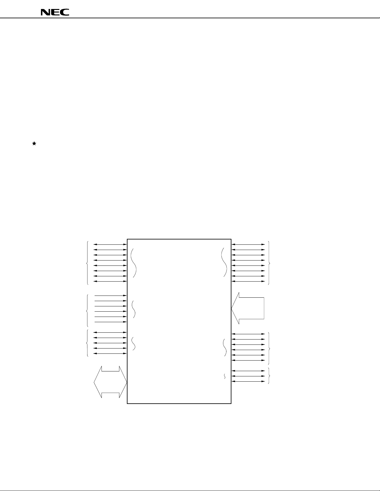
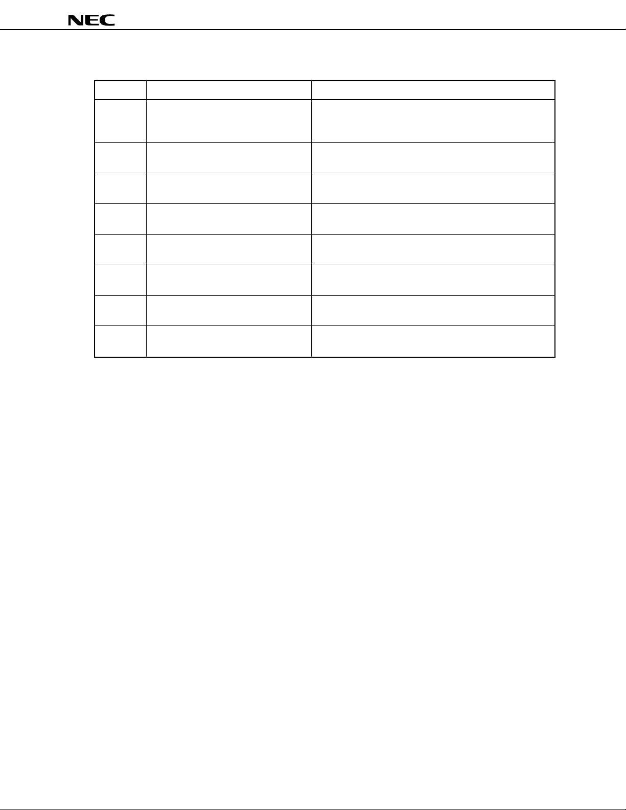
PD78362A is provided with the ports shown in Figure 3-1 for various control operations.
The
The functions of each port are listed in Table 3-1. These ports function not only as digital ports but also as
input/output lines of the internal hardware.
Port 0
Port 2
Port 3
Port 4
Figure 3-1. Port Configuration
P00
P07
P20
P25
P30
P34
8
P40-P47
P50
P57
P70-P77
P80
P85
P90
P92
Port 5
8
Port 7
Port 8
Port 9
26
µ
PD78361A, 78362A
Table 3-1. Functions of Each Port
Port Port function Multiplexed function
Port 0
Port 2
Port 3
Port 4
Port 5
Port 7
Port 8
Port 9
8-bit I/O port. Can be set in input or
output mode in 1-bit units.
6-bit input port.
5-bit I/O port. Can be set in input or
output in 1-bit units.
8-bit I/O port. Can be set in input or
output mode in 8-bit units.
8-bit I/O port. Can be set in input or
output mode in 1-bit units.
8-bit input port.
6-bit I/O port. Can be set in input or
output mode in 1-bit units.
3-bit I/O port. Can be set in input or
output mode in 1-bit units.
In control mode, serves as real-time output port (RTP), or
input operation control signal of real-time pulse unit (RPU)
and output PWM signal.
Inputs external interrupt and count pulse of real-time pulse
unit (RPU) (fixed to the control mode).
In control mode, inputs/outputs signals of serial interfaces
(UART, CSI).
—
—
Input analog signals to A/D converter (fixed to the control
mode).
In control mode, outputs timer of real-time pulse unit (RPU).
—
27
 Loading...