NEC uPD77114GC-xxx-9EU, uPD77113AF1-xxx-CN1 Datasheet

DATA SHEET
MOS INTEGRATED CIRCUIT
µµµµ
PD77113A, 77114
16-BIT FIXED-POINT DIGITAL SIGNAL PROCESSORS
DESCRIPTION
The µPD77113A and 77114 are 16-bit fixed-point digital signal processors (DSPs).
Compared with the µPD77016 family, these DSPs have improved power consumption and are ideal for battery-
powered mobile terminals such as PDAs and cellular phones.
Both mask ROM and RAM models are available.
For details of the functions of these DSPs, refer to the following User’s Manuals:
PD77111 Family User’s Manual : U14623E
µ
PD77016 Family User’s Manual - Instructions: U13116E
µ
FEATURES
Instruction cycle (operating clock)
z
PD77113A : 13.3 ns MIN (75 MHz MAX)
µ
PD77114 : 13.3 ns MIN (75 MHz MAX)
µ
Memory
z
• Internal instruction memory
PD77113A : RAM 3.5K words × 32 bits
µ
Mask ROM 48K words × 32 bits
PD77114 : RAM 3.5K words × 32 bits
µ
Mask ROM 48K words × 32 bits
• Data memory
PD77113A : RAM 16K words × 16 bits × 2 banks
µ
Mask ROM 32K words × 16 bits × 2 banks
PD77114 : RAM 16K words × 16 bits × 2 banks
µ
Mask ROM 32K words × 16 bits × 2 banks
External memory space 8K words × 16 bits × 2 banks
ORDERING INFORMATION
Part Number Package
PD77113AF1-xxx-CN1 80-pin plastic fine-pitch BGA (9 × 9)
µ
PD77114GC-xxx-9EU 100-pin plastic TQFP (fine pitch) (14 × 14)
µ
Remark
Document No. U14373EJ3V0DS00 (3rd edition)
Date Published February 2001 N CP(K)
Printed in Japan
xxx indicates ROM code suffix.
The information in this document is subject to change without notice. Before using this document, please
confirm that this is the latest version.
Not all devices/types available in every country. Please check with local NEC representative for
availability and additional information.
The mark shows major revised points.
©
1999
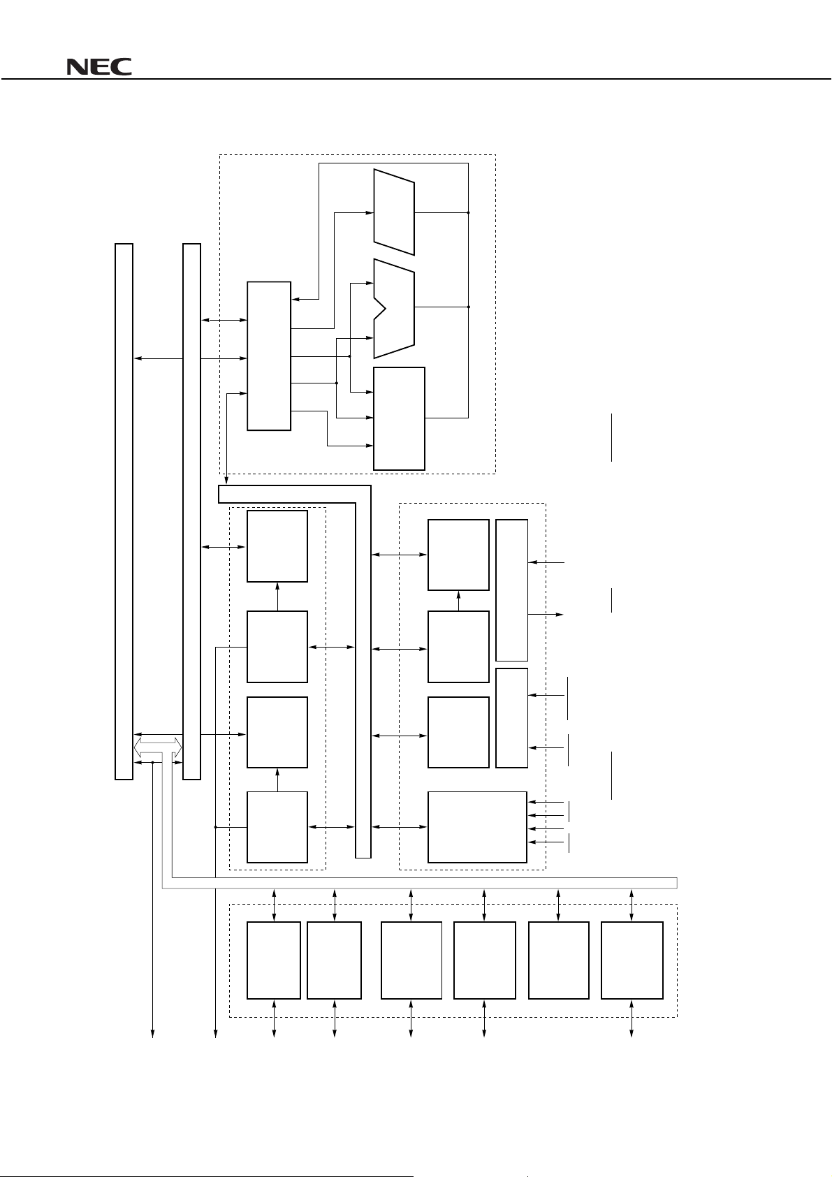
BLOCK DIAGRAM
BSFT
µµµµ
PD77113A, 77114
X bus
Y bus
R0 - R7
Y memory
data
addressing
unit
Main bus
ALU (40)
MAC
16 × 16 + 40 → 40
Program
control unit
Operation unit
Instruction
memory
PC stack
PLL
CLKOUT CLKIN
Note
WAKEUP
Interrupt
control
Host I/O
CPU control
Wait
RESET
Note
INT1 - INT4
controller
option.
Note The WAKEUP pin is multiplexed with the INT4 pin. The function of the WAKEUP pin can be activated or deactivated by mask
IE
I/O
X memory Y memory
Data memory unit
X memory
data
addressing
unit
Serial
I/O #1
Peripheral units
External memory
2
Serial
I/O #2
Data Sheet U14373EJ3V0DS
Port
Loop control
stack
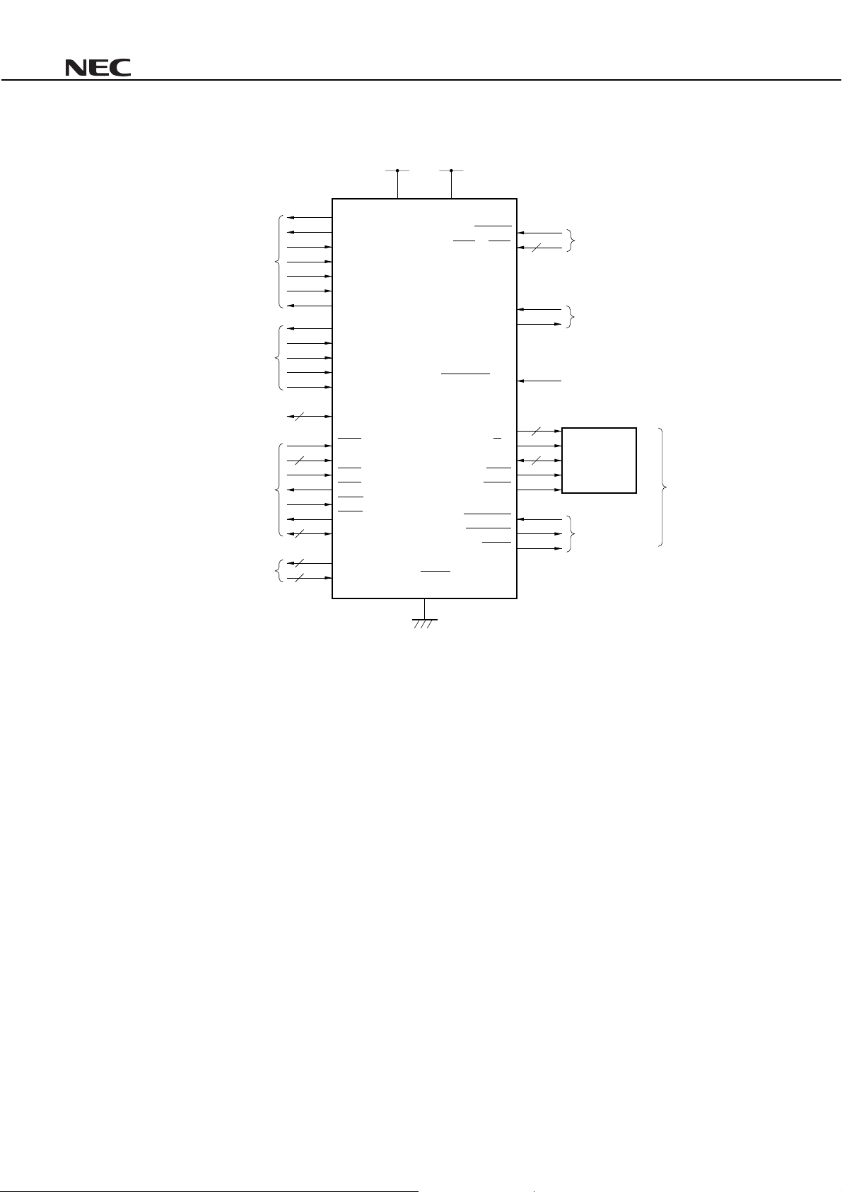
PIN CONFIGURATION
Serial interface #1
Serial interface #2
SO1
SORQ1
SOEN1
SCK1
SI1
SIEN1
SIAK1
SO2
SOEN2
SCK2
SI2
SIEN2
+2.5 V +3 V
IV
DD
EV
WAKEUP
DD
RESET
INT1 - INT4
CLKIN
CLKOUT
Note 1
(4)
µµµµ
PD77113A, 77114
Reset, interrupt
Clock
System control
Notes 1.
Port
Host interface
For debugging
P0 - P3
(4)
HCS
HA0, HA1
(2)
HRD
HRE
HWR
HWE
HD0 - HD7
(8)
TDO, TICE
(2)
TCK, TDI, TMS, TRST
(4)
GND
DA0 - DA12
X/Y
D0 - D15
MRD
MWR
HOLDRQ
HOLDAK
BSTB
(13)
(16)
The function of this pin can be activated or deactivated by mask option.
An external data memory interface is not provided on the
2.
PD77113A.
µ
External data
memory
Note 2
Data bus
control
Data Sheet U14373EJ3V0DS
3
4
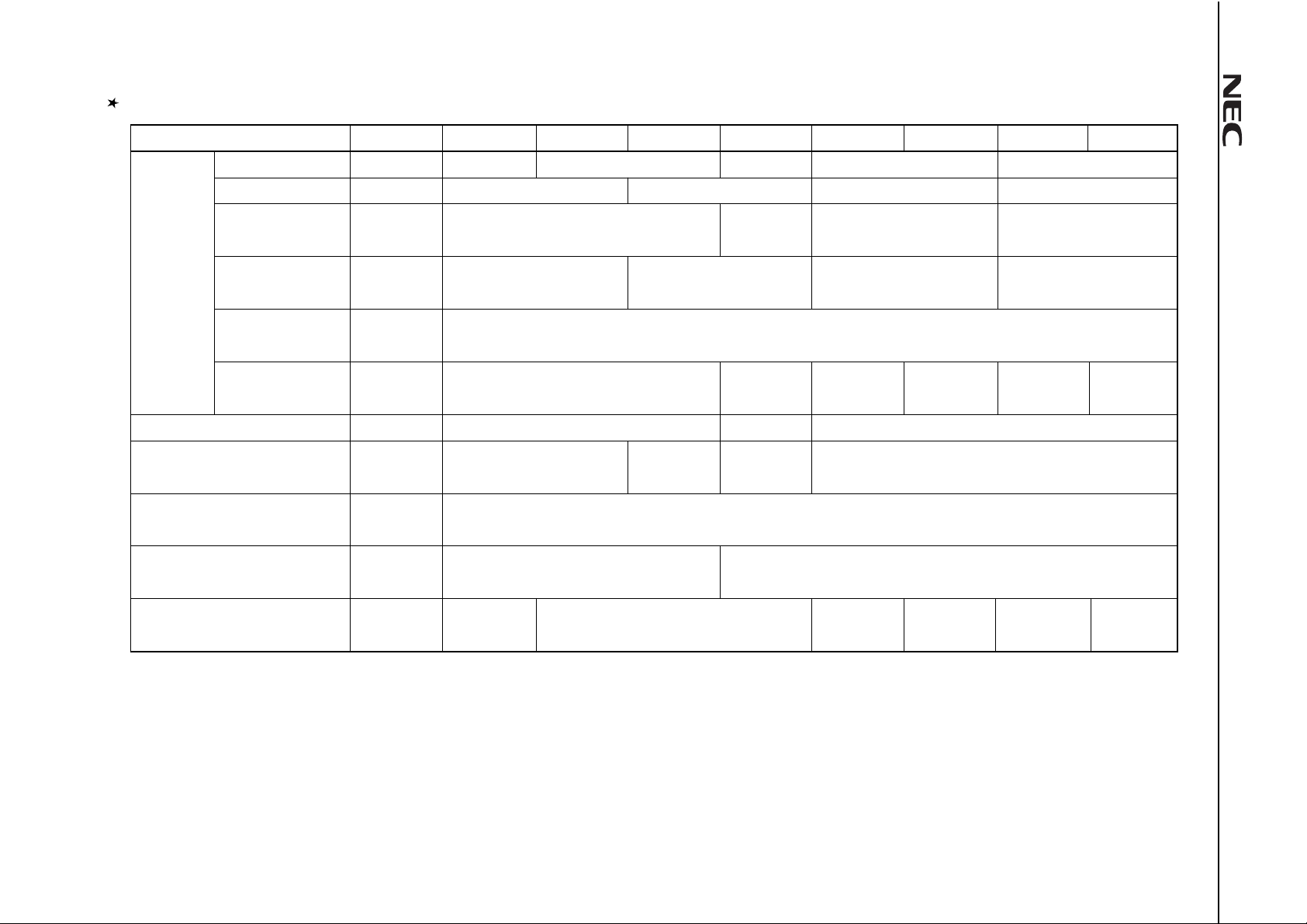
DSP FUNCTION LIST
Item PD77016
Memory space
(words × bits)
Data Sheet U14373EJ3V0DS
Instruction cycle (at maximum speed)
Multiple
Serial interface (two channels)
Supply voltage
Internal instruction RAM
Internal instruction ROM
Data RAM
(X/Y memory)
Data ROM
(X/Y memory)
External instruction
memory
External data memory
(X/Y memory)
µµµµµ µ µ
1.5K × 32 256 × 32 4K × 32 1K × 32
None
2K × 16 each 3K × 16 each 3K × 16 each
None 12K × 16 each 16K × 16 each
48K × 32
48K × 16 each 16K × 16 each None 16K × 16 each
30 ns (33 MHz)
–
Channels 1 and 2
have same function.
5 V 3 V DSP core: 2.5 V
×1, 2, 3, 4, 8 (mask option) Fixed to ×4 Integer of ×1 to 16 (mask option)
Channel 1 has same function as PD77016. Channel 2 does not have SORQ2 and SIAK2 pins (for connection of codec).
PD77019 PD77018A PD77019-013 PD77111 PD77112
24K × 32 None
16.6 ns (60 MHz) 13.3 ns (75 MHz)
µ
PD77110
35.5K × 32
24K × 16 each
None
32K × 16 each
15.3 ns (65 MHz)
Integer of ×1 to 8
(external pin)
31.75K × 32
None
I/O pins : 3 V
µµ
PD77113A PD77114
3.5K × 32
48K × 32
16K × 16 each
32K × 16 each
None 8K × 16 each
Package
160-pin QFP
116-pin BGA
100-pin TQFP 80-pin TQFP
80-pin FBGA
100-pin TQFP100-pin TQFP
80-pin FBGA 100-pin TQFP
µµ
µ
µ
PD77113A, 77114
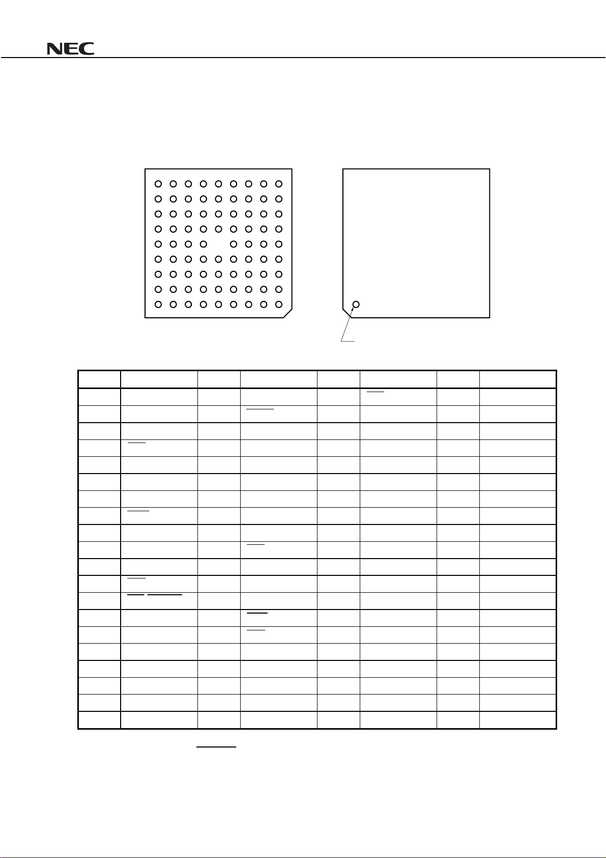
PIN CONFIGURATION
µµµµ
PD77113A, 77114
80-pin plastic fine-pitch BGA (9
PD77113AF1-xxx-CN1
µµµµ
9)
××××
(Bottom View) (Top View)
9
8
7
6
5
4
3
2
1
JHGFEDCBA ABCDEFGHJ
Index mark
Pin No. Pin Name Pin No. Pin Nam e Pin No. Pin Name Pin No. Pin Nam e
A1
−
C3 NU E6 HCS G8 P1
A2 NU C4 RESET E7 GND G9 GND
A3 EV
DD
C5 TDI E8 HD1 H1 NU
A4 INT3 C6 TDO E9 HD2 H2 NU
A5 GND C7 CLKIN F1 NU H3 SCK1
A6 TMS C8 HA0 F2 NU H4 SOEN2
A7 GND C9 EV
A8 TRST D1 EV
A9
−
D2 NU F5 HD0 H7 P0
DD
DD
F3 SOEN1 H5 SIEN2
F4 GND H6 P3
B1 NU D3 INT2 F6 SI2 H8 HD7
B2 NU D4 NU F7 HD3 H9 NU
B3 INT1 D5 TCK F8 HD6 J1
B4
B5 IV
INT4/WAKEUP
DD
Note
D6 GND F9 HD5 J2 NU
D7 HWR G1 EV
DD
J3 SI1
−
B6 TICE D8 HRD G2 GND J4 SORQ1
B7 IV
DD
D9 EV
DD
G3 SIEN1 J5 SO2
B8 HA1 E1 NU G4 SO1 J6 SCK2
B9 CLKOUT E2 GND G5 IV
DD
J7 EV
DD
C1 GND E3 SIAK1 G6 HD4 J8 NU
C2 NU E4 NU G7 P2 J9
−
The function of the WAKEUP pin can be activated or deactivated by a mask option.
Note
Data Sheet U14373EJ3V0DS
5
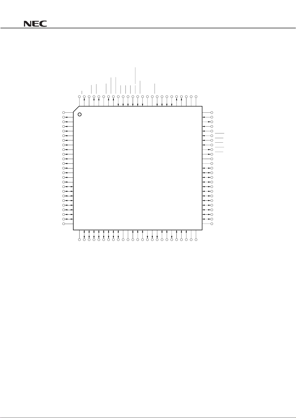
µµµµ
PD77113A, 77114
100-pin plastic TQFP (fine-pitch) (14
PD77114GC-xxx-9EU
µµµµ
EVDDX/Y
I.C.
MRD
100
999897969594939291908988878685848382818079787776
GND
NC
NC
DA12
DA11
DA10
DA9
DA8
DA7
DA6
DA5
DA4
DA3
DA2
DA1
DA0
D15
D14
D13
D12
D11
D10
D9
D8
EV
DD
1
2
3
4
5
6
7
8
9
10
11
12
13
14
15
16
17
18
19
20
21
22
23
24
25
26272829303132333435363738394041424344454647484950
14) (Top View)
××××
MWRNCBSTB
HOLDAK
HOLDRQ
INT1
INT2
Note
INT3
INT4/WAKEUP
RESET
GND
IVDDTRST
TMS
TDI
TCK
TICE
TDO
GND
IVDDGND
75
74
73
72
71
70
69
68
67
66
65
64
63
62
61
60
59
58
57
56
55
54
53
52
51
EV
DD
CLKIN
CLKOUT
HA1
HA0
HWR
HRD
HCS
HWE
HRE
GND
DD
EV
HD0
HD1
HD2
HD3
HD4
HD5
HD6
HD7
P0
P1
P2
P3
GND
D7D6D5D4D3D2D1
GND
The functions can be activated or deactivated by a mask option.
Note
D0
DD
SI1
IV
GND
SIEN1
SCK1
SIAK1
SO1
SOEN1
SOEN2
SORQ1
SO2
SCK2
SIEN2
SI2
NC
DD
EV
6
Data Sheet U14373EJ3V0DS
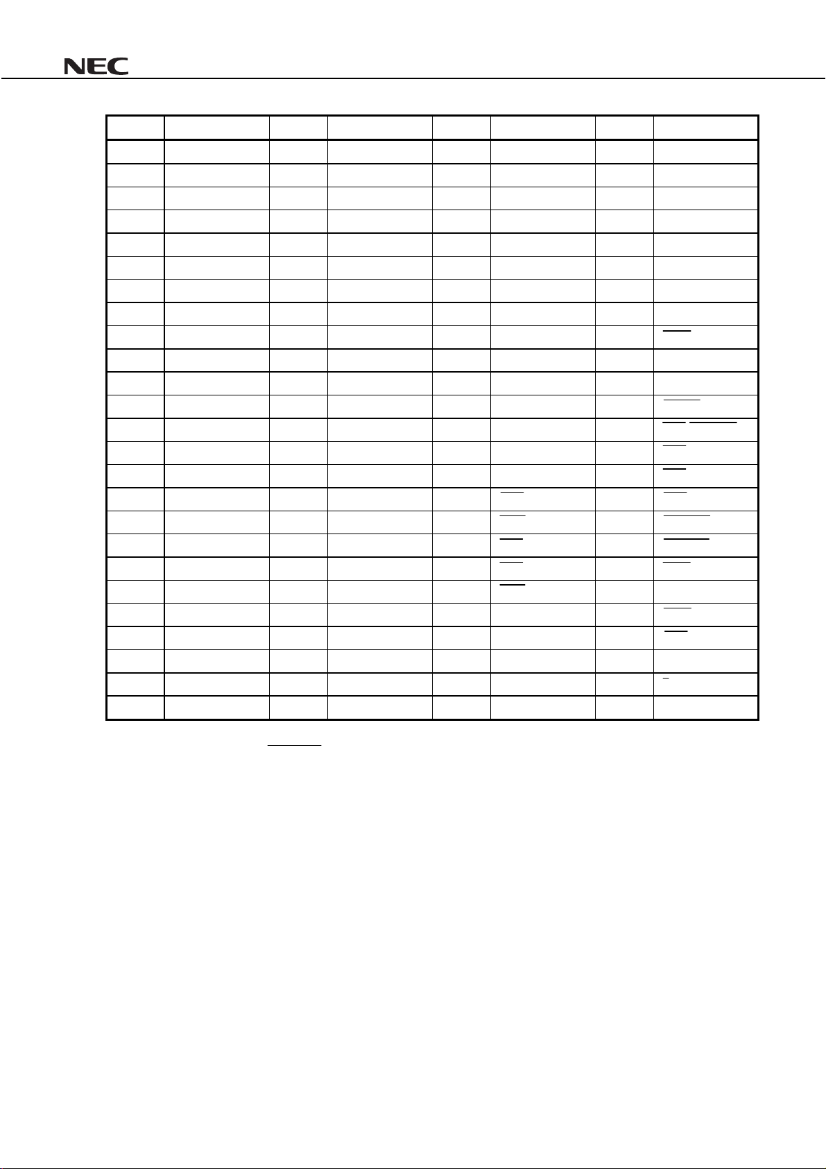
µµµµ
PD77113A, 77114
Pin No. Pin Name Pin No. Pin Nam e Pin No. Pin Name Pin No. Pin Nam e
1 GND 26 GND 51 GND 76 GND
2 NC 27D7 52P3 77IV
DD
3 NC 28D6 53P2 78GND
4 DA12 29D5 54P1 79TDO
5 DA11 30D4 55P0 80TICE
6 DA10 31D3 56HD7 81TCK
7 DA9 32 D2 57 HD6 82 TD1
8 DA8 33 D1 58 HD5 83 TMS
9 DA7 34 D0 59 HD4 84 TRST
10 DA6 35 I V
DD
60 HD3 85 IV
DD
11 DA5 36 GND 61 HD2 86 GND
12 DA4 37 SI1 62 HD1 87 RESET
13 DA3 38 S IEN1 63 HD0 88
14 DA2 39 S CK1 64 EV
DD
89 INT3
INT4/WAKEUP
15 DA1 40 SIAK1 65 GND 90 INT2
16 DA0 41 SO1 66 HRE 91 INT1
17 D15 42 S ORQ1 67 HWE 92 HOLDRQ
18 D14 43 S OEN1 68 HCS 93 HOLDAK
19 D13 44 S OEN2 69 HRD 94 BSTB
20 D12 45 S O2 70 HWR 95 NC
21 D11 46 S CK2 71 HA0 96 MWR
22 D10 47 S IEN2 72 HA1 97 MRD
23 D9 48 SI2 73 CLKOUT 98 I.C.
24 D8 49 NC 74 CLKIN 99 X/Y
25 EV
DD
50 E V
DD
75 E V
DD
100 EV
DD
Note
The function of the WAKEUP pin can be activated or deactivated by a mask option.
Note
Data Sheet U14373EJ3V0DS
7

PIN NAME
BSTB : Bus Strobe
CLKIN : Clock Input
CLKOUT : Clock Output
D0 - D15 : 16-bit Data Bu s
DA0 - DA12 : External Data Memory Address Bus
DD
EV
GND : Ground
HA0, HA1 : Host Data Access
HCS : Host Chip Select
HD0 - HD7 : Host Data Bus
HOLDAK : Hold Acknowledge
HOLDRQ : Hold Request
HRD : Host Read
HRE : Host Read Enable
HWE : Host Write Enable
HWR : Host Write
I.C. : Internally Connected
INT1 - INT4 : Interrupt
DD
IV
MRD : Memory Read Output
MWR : Memory Wri te Output
NC : Non-Connection
NU : Not Used
P0 - P3 : Port
RESET : Reset
SCK1, SCK2 : Serial Clock Input
SI1, SI2 : Serial Data Input
SIAK1 : Serial Input Acknowledge
SIEN1, SIEN2 : Serial Input Enable
SO1, SO2 : Serial Data Output
SOEN1, SOEN2: Serial Output Enable
SORQ1 : Serial Output Request
TCK : Test Clock Input
TDI : Test Data Input
TDO : Test Data Output
TICE : Test In-Circuit Emulator
TMS : Test Mode Select
TRST : Test Reset
WAKEUP : Wakeup from STOP Mode
X/Y : X/Y Memory Select
: Power Supply for I/O Pins
: Power Supply for DSP Core
µµµµ
PD77113A, 77114
8
Data Sheet U14373EJ3V0DS

µµµµ
PD77113A, 77114
CONTENTS
1. PIN FUNCTION................................................................................................................................. 10
1.1 Pin Function Description.......................................................................................................... 10
1.2 Connection of Unused Pins ..................................................................................................... 15
2. FUNCTION OUTLINE....................................................................................................................... 17
2.1 Program Control Unit................................................................................................................ 17
2.2 Arithmetic Unit........................................................................................................................... 18
2.3 Data Memory Unit...................................................................................................................... 19
2.4 Peripheral Units......................................................................................................................... 19
3. CLOCK GENERATOR...................................................................................................................... 20
4. RESET FUNCTION........................................................................................................................... 20
4.1 Hardware Reset ......................................................................................................................... 20
4.2 Initializing PLL........................................................................................................................... 21
5. FUNCTIONS OF BOOT-UP ROM...................................................................................................21
5.1 Boot at Reset ............................................................................................................................. 21
5.2 Reboot ........................................................................................................................................ 22
5.3 Signature Operation.................................................................................................................. 23
5.4 Instruction ROM Modification.................................................................................................. 23
6. STANDBY MODES........................................................................................................................... 24
6.1 HALT Mode................................................................................................................................. 24
6.2 STOP Mode ................................................................................................................................ 24
7. MEMORY MAP.................................................................................................................................. 25
7.1 Instruction Memory ................................................................................................................... 25
7.2 Data Memory.............................................................................................................................. 27
8. MASK OPTION ................................................................................................................................. 28
8.1 Clock Control Options.............................................................................................................. 28
8.2 WAKEUP Function .................................................................................................................... 29
9. INSTRUCTIONS................................................................................................................................. 30
9.1 Outline of Instructions.............................................................................................................. 30
9.2 Instruction Set and Operation.................................................................................................. 31
10. ELECTRICAL SPECIFICATIONS..................................................................................................... 37
11. PACKAGE DRAWINGS.................................................................................................................... 56
12. RECOMMENDED SOLDERING CONDITIONS............................................................................... 58
Data Sheet U14373EJ3V0DS
9

µµµµ
PD77113A, 77114
1. PIN FUNCTION
Because the pin numbers differ depending on the package, refer to the diagram of the package to be used.
1.1 Pin Function Description
• Power supply
Pin Name
DD
IV
DD
EV
GND 1, 26, 36, 51,
Remark
100-pin TQFP 80-pin BGA
35, 77, 85 B5, B7, G5
25, 50, 64, 75,
100
65, 76, 78, 86
Please supply voltage to the IV
Pin No.
A3, C9, D1, D9,
G1, J7
A5, A7, C1, D6,
E2, E7, F4, G2,
G9
I/O Function Shared by:
Power to DSP core (+2.5 V)
−
Power to I/O pins (+3 V)
−
Ground
−
DD
and EVDD pins simultaneously.
• System control
Pin Name
100-pin TQFP 80-pin BGA
CLKIN 74 C7 Input System clock i nput
CLKOUT 73 B9 Output Internal system clock output
RESET 87 C4 Input Internal system reset signal input
WAKEUP 88 B4 Input St op mode releas e signal input.
Pin No.
I/O Function Shared by:
• When this pin is asserted active, the stop
mode is released. The functi on of this pin
can be activated or deacti vated by a mask
option.
−
−
−
−
−
INT4
• Interrupt
Pin Name
100-pin TQFP 80-pin BGA
INT1 - INT3 91 - 89 B3, D3, A4 Input
INT4 88 B4 Input
10
Pin No.
Data Sheet U14373EJ3V0DS
I/O Function Shared by:
External maskable int errupt input.
• Detected at the fall i ng edge.
−
WAKEUP

µµµµ
PD77113A, 77114
• External data memory interface (
Pin No.
Pin Name
100-pin TQFP 80-pin BGA
X/Y 99
DA0 - DA12 16 - 4
D0 - D15 34 - 27, 24 - 17
MRD 97
MWR 96
HOLDRQ 92
BSTB 94
HOLDAK 93
PD77114 only)
µµµµ
−
−
−
−
−
−
−
−
I/O Function Shared by:
Output
(3S)
Output
(3S)
I/O
(3S)
Output
(3S)
Output
(3S)
Input Hold request signal
Output Bus strobe si gnal
Output Hold acknowledge signal
Memory select signal output.
0: Uses X memory.
1: Uses Y memory.
Address bus of external data memory.
• Accesses the external memory.
• Continuously outputs the external memory
address accessed las t when the external
memory is not being accessed. Kept low
(0x000) if the external memory is never
accessed after reset.
16-bit data bus.
• Accesses the external memory.
Read output
• External memory read
Write output
• External memory write
• Input a low level to t hi s pin when the external
device uses the external data memory bus of
the
PD77114.
µ
• This pin goes l ow when the
the external data memory bus .
• This pin goes low when the ex t ernal device
is enabled to use the external data memory
bus of the
PD77114.
µ
PD77114 uses
µ
−
−
−
−
−
−
−
−
Remark
Pins marked “3S” under the heading “I/O” go into a high-impedance state in the following conditions:
X/Y, DA0-DA12, MRD, MWR: When the bus is released (HOLDAK = low level)
D0-D15: When the external data memory is not being accessed and when the bus is released
(HOLDAK = low level)
Data Sheet U14373EJ3V0DS
11

• Serial interface
µµµµ
PD77113A, 77114
Pin Name
SCK1 39 H3 Input Serial 1 cloc k input
SORQ1 42 J4 Output Serial output 1 request
SOEN1 43 F3 Input Serial output 1 enable
SO1 41 G4 Output
SIEN1 38 G3 Input Serial input 1 enable
SI1 37 J3 Input Serial data input 1
SIAK1 40 E3 Output Serial i nput 1 acknowledge
SCK2 46 J6 Input Serial 2 clock input
SOEN2 44 H4 Input Serial output 2 enable
SO2 45 J5 Output
SIEN2 47 H5 Input Serial input 2 enable
SI2 48 F6 Input Serial data input 2
Remark
100-pin TQFP 80-pin BGA
The pins marked “3S” under the heading “I/O” go into a high-impedance state on completion of data
Pin No.
I/O Function Shared by:
Serial data output 1
(3S)
Serial data output 2
(3S)
transfer and input of the hardware reset (RESET) signal.
−
−
−
−
−
−
−
−
−
−
−
−
12
Data Sheet U14373EJ3V0DS

• Host interface
µµµµ
PD77113A, 77114
Pin Name
100-pin TQFP 80-pin BGA
HA1 72 B8 Input Spec i fies the register to be accessed by HD7
HA0 71 C8 Input Spec i fies the register to be accessed by HD7
HCS 68 E6 Input Chip select input
HRD 69 D8 Input Host read input
HWR 70 D7 Input Host write input
HRE 66
HWE 67
HD0 - HD7 63 - 56 F5, E8, E9, F7,
Pin No.
G6, F9, F8, H8
I/O Function Shared by:
through HD0.
• 1: Accesses the hos t i nterface status
register (HST).
• 0: Accesses the hos t transmit data register
(HDT (out)) when read (HRD = 0), and
host receive data regist er (HDT (i n))
when written (HWR = 0).
through HD0.
• 1: Accesses bits 15 through 8 of HST, HDT
(in), and HDT (out).
• 0: Accesses bits 7 through 0 of HST, HDT
(in), and HDT (out).
−
−
Output Host read enable output
Output Host write enable output
I/O
(3S)
8-bit host data bus
−
−
−
−
−
−
−
−
Remark
The pins marked “3S” under the heading “I/O” go into a high-impedance state when the host interface is
not being accessed.
• I/O ports
Pin Name
100-pin TQFP 80-pin BGA
P0 55 H7 I/O
P1 54 G8 I/O
P2 53 G7 I/O
P3 52 H6 I/O
Pin No.
I/O Function Shared by:
General-purpose I/O port
−
−
−
−
Data Sheet U14373EJ3V0DS
13

• Debugging interface
µµµµ
PD77113A, 77114
Pin Name
100-pin TQFP 80-pin BGA
TDO 79 C6 Output
TICE 80 B6 Output
TCK 81 D5 Input
TDI 82 C5 Input
TMS 83 A6 Input
TRST 84 A8 Input
Pin No.
I/O Function Shared by:
• Others
Pin Name
100-pin TQFP 80-pin BGA
I.C. 98
NU
NC 2, 3, 49, 95
−−
Pin No.
−−
−
A2, B1, B2, C2,
C3, D2, D4, E1,
E4, F1, F2, H1,
H2, H9, J2, J8
−−
A1, A9, J1, J9
I/O Function Shared by:
For debugging
Internally connected. Leave this pin
unconnected.
No function pins. Connect to EV
−
resistor, or connect to GND via pull-down
resistor.
No-connect pins. Leave these pins
unconnected.
Pins to strengthen sol deri ng. Connect these
−
pins to the board as necessary.
DD
via pull-up
−
−
−
−
−
−
−
−
−
−
Caution If any signal is input to these pins or if an attempt is made to read these pins, the normal
operation of the
PD77113A and 77114 is not guaranteed.
µµµµ
14
Data Sheet U14373EJ3V0DS

1.2 Connection of Unused Pins
1.2.1 Connection of Function Pins
When mounting, connect unused pins as follows:
Pin I/O Recommended Connection
INT1 - INT4 Input Connect to EVDD.
X/Y Output
DA0 - DA12 Output
D0 - D15
MRD, MWR Output Leave unconnected.
HOLDRQ Input Leave unconnected. (i nternally pulled up).
BSTB, HOLDAK Output Leave unconnected.
SCK1, SCK2 Input
SI1, SI2 Input
SIEN1, SIEN2 Input
SOEN1, SOEN2 Input
SORQ1 Output
SO1, SO2 Output
SIAK1 Output
HA0, HA1 Input Connect to EVDD or GND.
HCS, HRD, HWR Input Connec t to EVDD.
HRE, HWE Output Leave unconnected.
HD0 - HD7
P0 - P3 I/O
TCK Input Connect to GND via pull-down resistor.
TDO, TICE Out put Leave unconnected.
TMS, TDI Input Leave unconnected. (internally pulled up).
TRST Input Leave unconnected. (internal l y pul l ed down).
CLKOUT Output Leave unconnected.
Note 1
Note 2
I/O Connect to E VDD via pull-up resistor, or c onnect to GND via pull-down resistor.
I/O
Leave unconnected.
DD
Connect to EV
Connect to GND.
Leave unconnected.
Connect to EV
or GND.
DD
via pull-up resistor, or c onnect to GND via pull-down resistor.
µµµµ
PD77113A, 77114
Notes 1.
These pins may be left unconnected if the external data memory is not accessed in the program.
However, connect these pins as recommended in the halt and stop modes when the power
consumption must be lowered.
These pins may be left unconnected if HCS, HRD, and HWR are fixed to the high level.
2.
However, connect these pins as recommended in the halt and stop modes when the power
consumption must be lowered.
Data Sheet U14373EJ3V0DS
15

1.2.2 Connection of no-function pins
Pin I/O Recommended Connection
µµµµ
PD77113A, 77114
I.C.
NU
NC
−
−
−
Leave unconnected.
Connect to EVDD via pull-up resistor, or c onnect to GND via pull-down resistor.
Leave unconnected.
16
Data Sheet U14373EJ3V0DS

µµµµ
PD77113A, 77114
2. FUNCTION OUTLINE
2.1 Program Control Unit
This unit is used to execute instructions, and control branching, loops, interrupts, the clock, and the standby mode
of the DSP.
2.1.1 CPU control
A three-stage pipeline architecture is employed and almost all the instructions, except some instructions such as
branch instructions, are executed in one system clock.
2.1.2 Interrupt control
Interrupt requests input from external pins (INT1 through INT4) or generated by the internal peripherals (serial
interface and host interface) are serviced. The interrupt of each interrupt source can be enabled or disabled.
Multiple interrupts are also supported.
2.1.3 Loop control task
A loop function without any hardware overhead is provided. A loop stack with four levels is provided to support
multiple loops.
2.1.4 PC stack
A 15-level PC stack that stores the program counter supports multiple interrupts and subroutine calls.
2.1.5 PLL
A PLL is provided as a clock generator that can multiply or divide an external clock input to supply an operating
clock to the DSP. A multiple of ×1 to ×16 or a division ratio of 1/1 to 1/16 can be set by a mask option.
Two standby modes are available for lowering the power consumption while the DSP is not in use.
• HALT mode : Set by execution of the HALT instruction. The current consumption drops to several mA. The
normal operation mode is recovered by an interrupt or hardware reset.
• STOP mode: Set by execution of the STOP instruction. The current consumption drops to several 10 µA. The
normal operation mode is recovered by hardware reset or WAKEUP pin
If the WAKEUP function is activated by mask option
Note
2.1.6 Instruction memory
The capacity and type of the memory differ depending on the model of the DSP.
64 words of the instruction RAM are allocated to interrupt vectors.
A boot-up ROM that boots up the instruction RAM is provided, and the instruction RAM can be initialized or
rewritten by self boot (boot from the internal data ROM or external data space) or host boot (boot via host interface).
The µPD77113A and 77114 have 3.5K-word instruction RAM and 48K-word instruction ROM.
Note
.
Data Sheet U14373EJ3V0DS
17

µµµµ
PD77113A, 77114
2.2 Arithmetic Unit
This unit performs multiplication, addition, logical operations, and shift, and consists of a 40-bit multiply
accumulator, 40-bit data ALU, 40-bit barrel shifter, and eight 40-bit general-purpose registers.
2.2.1 General-purpose registers (R0 through R7)
These eight 40-bit registers are used to input/output data for arithmetic operations, and load or store data from/to
data memory.
A general-purpose register (R0 to R7) is made up of three parts: R0L through R7L (bits 15 through 0), R0H
through R7H (bits 31 through 16), and R0E through R7E (bits 39 through 32). Depending on the type of operation,
RnL, RnH, and RnE are used as one register or in different combinations.
2.2.2 Multiply accumulator (MAC)
The MAC multiplies two 16-bit values, and adds or subtracts the multiplication result from one 40-bit value, and
outputs a 40-bit value.
The MAC is provided with a shifter (MSFT: MAC ShiFTer) at the stage preceding the input stage. This shifter can
arithmetically shift the 40-bit value to be added to or subtracted from the multiplication result 1 or 16 bits to the right .
2.2.3 Arithmetic logic unit (ALU)
This unit inputs one or two 40-bit values, executes an arithmetic or logical operation, and outputs a 40-bit value.
2.2.4 Barrel shifter (BSFT: Barrel ShiFTer)
The barrel shifter inputs a 40-bit value, shifts it to the left or right by any number of bits, and outputs a 40-bit value.
The data may be arithmetically shifted to the right shifted to the right, in which case the data is sign-extended, or
logically shifted to the right, in which case 0 is inserted from the MSB.
18
Data Sheet U14373EJ3V0DS

µµµµ
PD77113A, 77114
2.3 Data Memory Unit
The data memory unit consists of two banks of data memory and two data addressing units.
2.3.1 Data memory
The capacity and type of the memory differ depending on the model of the DSP. All DSPs have two banks of data
memory (X data memory and Y data memory). A 64-word peripheral area is assigned in the data memory space.
The µPD77113A and 77114 have 16K words × 2 banks data RAM and 32K words × 2 banks data ROM.
In addition, the µPD77114 has an external data memory interface so that the external memory can be expanded
to 8K words × 2 banks.
2.3.2 Data addressing unit
An independent data addressing unit is provided for each of the X data memory and Y data memory spaces.
Each data addressing unit has four data pointers (DPn), four index registers (DNn), one modulo register (DMX or
DMY), and an address ALU.
2.4 Peripheral Units
A serial interface, host interface, general-purpose I/O port, and wait cycle register are provided. All these internal
peripherals are mapped to the X data memory and Y data memory spaces, and are accessed from program as
memory-mapped I/Os.
2.4.1 Serial interface (SIO)
Two serial interfaces are provided. These serial interfaces have the following features:
• Serial clock : Supplied from external source to each interface. The same clock is used for input and output
on the interface.
• Frame length: 8 or 16 bits, and MSB or LSB first selectable for each interface and input or output
• Handshake : Handshaking with external devices is implemented with a dedicated status signal. With the
internal units, polling, wait, or interrupt are used.
2.4.2 Host interface (HIO)
This is an 8-bit parallel port that inputs data from or outputs data to an external host CPU or DMA controller. In
the DSP, a 16-bit register is mapped to memory for input data, output data, and status. Handshaking with an external
device is implemented by using a dedicated status signal. Handshaking with internal units is achieved by means of
polling, wait, or interrupts.
2.4.3 General-purpose I/O port (PIO)
This is a 4-bit I/O port that can be set in the input or output mode in 1-bit units.
2.4.4 Wait cycle register
The number of wait cycles to be inserted when the external data memory area is accessed can be specified in
advance by using a register (DWTR)
This function is not available on the µPD77113A because this DSP does not have an external data area.
Note
Note
. The number of wait cycles that can be set is 1, 3, or 7.
Data Sheet U14373EJ3V0DS
19
 Loading...