
DATA SHEET
MOS INTEGRATED CIRCUIT
µ
PD77016
16 bits, Fixed-point Digital Signal Processor
µ
PD77016 is a 16 bits fixed-point DSP (Digital Signal Processor) developed for digital signal processing with its
demand for high speed and precision.
FEATURES
• FUNCTIONS
• Instruction cycle: 30 ns (MIN.) with 33 MHz clock
• Dual load/store
• Hardware loop function
• Conditional execution
• Executes product-sum operation in one instruction cycle
• PROGRAMMING
• 16 bits × 16 bits + 40 bits → 40 bits multiply accumulator
• 8 general registers (40 bits each)
• 8 ROM/RAM data pointer: each data memory area has 4 registers
• 10 source interrupts (external: 4, internal: 6)
• 3 operand instructions (example: R0 = R0 +R1L∗R2L)
• Nonpipeline on execution stage
• MEMORY AREAS
• Program memory area: 64K words × 32 bits
• Two independent data memory areas: 64K words × 16 bits (X/Y memory)
• ON-CHIP PERIPHERAL
• I/O port: 4 bits
• Serial I/O (16 bits): 2 channels
• CMOS
• +5 V single power supply
ORDERING INFORMATION
Part Number Package
µ
PD77016GM-KMD 160-pin plastic QFP (FINE PITCH) (24 × 24 mm)
Document No. U10891EJ5V0DS00 (5th edition)
Date Published April 1998 N CP(K)
Printed in Japan
The information in this document is subject to change without notice.
The mark shows major revised points.
©
1992, 1994, 1995

2
X–Bus
BLOCK DIAGRAM
External
Memory
Serial
I/O #1
Serial
I/O #2
Ports
Host I/O
X Memory
Data
Pointers
Interrupt
Control
X Memory
2KW–RAM
Loop
Control
Stack
CPU Control
Main Bus
Y Memory
Data
Pointers
PC Stack
Y–Bus
Y Memory
2KW–RAM
Instruction
Memory
(1.5 KW–RAM)
MPY
16 × 16 + 40 → 40
R0–R7
ALU (40)
Wait
Controller
IE
I/O
INT1–INT4 RESET CLKOUT CLKIN
External Instruction MemoryWAIT
µ
PD77016

FUNCTIONAL PIN GROUPS
SO1
SORQ1
SOEN1
SCK1
SI1
SIEN1
SIAK1
Serial
Interface #1
SO2
SORQ2
SOEN2
SCK2
SI2
SIEN2
SIAK2
Serial
Interface #2
HCS
HA0,HA1
HRD
HRE
HWR
HWE
HD0 - HD7
Host Interface
P0 - P3Ports
(2)
(4)
(8)
V
DD
+5 V
GND
RESET
INT1
INT2
INT3
INT4
IA0 - IA15
ID0 - ID31
HOLDRQ
BSTB
X/Y
DA0 - DA15
D0 - D15
WAIT
MRD
MWR
HOLDAK
External Instruction
Memory
Data Bus Control
Interrupts
(16)
(32)
(16)
External Data Memory
(16)
(2)
(3)
TDO,TICE
TCK,TDI,TMS
CLKIN
CLKOUT
PWR
Debugging
Interface
µ
PD77016
3
4
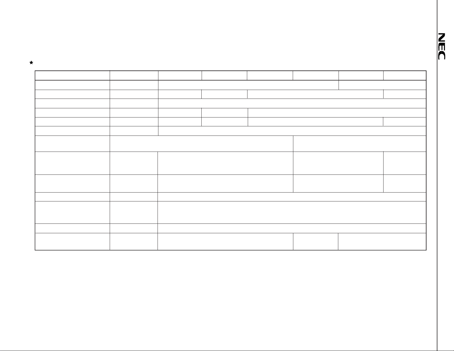
Functional Differences among the
Item
Internal instruction RAM 1.5K words 256 words 4K words
Internal instruction ROM None 4K words 12K words 24K words None
External instruction memory 48K words None
Data RAM (X/Y memory) 2K words each 1K words each 2K words each 3K words each
Data ROM (X/Y memory) None 2K words each 4K words each 12K words each None
External data memory 48K words each 16K words each
Instruction cycle
(Maximum operation speed)
External clock
(at maximum operation speed)
Crystal
(at maximum operation speed)
Instruction – STOP instruction is added.
Serial interface (2 Channels)
Power supply 5V 3 V
Package
µ
PD7701× Family
µ
PD77016
66 MHz
–
Channel 1 has the
same functions
as channel 2.
160-pin plastic QFP 100-pin plastic TQFP
µ
PD77015
30 ns (33 MHz)
Variable multiple rate (1, 2, 4, 8 ) by mask option.
Channel 1 has the same functions as that of the
Channel 2 has no SORQ2 or SIAK2 pin (Channel 2 is used for CODEC connection).
µ
PD77017
33/16.5/8.25/4.125 MHz
33 MHz
µ
PD77018
µ
PD77016.
µ
PD77018A
60/30/20/15/7.5 MHz
Variable multiple rate (1, 2, 3, 4, 8 ) by
mask option.
60 MHz
100-pin plastic TQFP
116-pin plastic BGA
µ
PD77019
16.6 ns (60 MHz)
100-pin plastic TQFP
µ
PD77019-013
15 MHz
Multiple rate is
fixed to 4.
–
Remark The
µ
PD77019-013 internal ROM area is masked already by the void code to use as RAM based DSP without mask code ordering process.
µ
PD77016
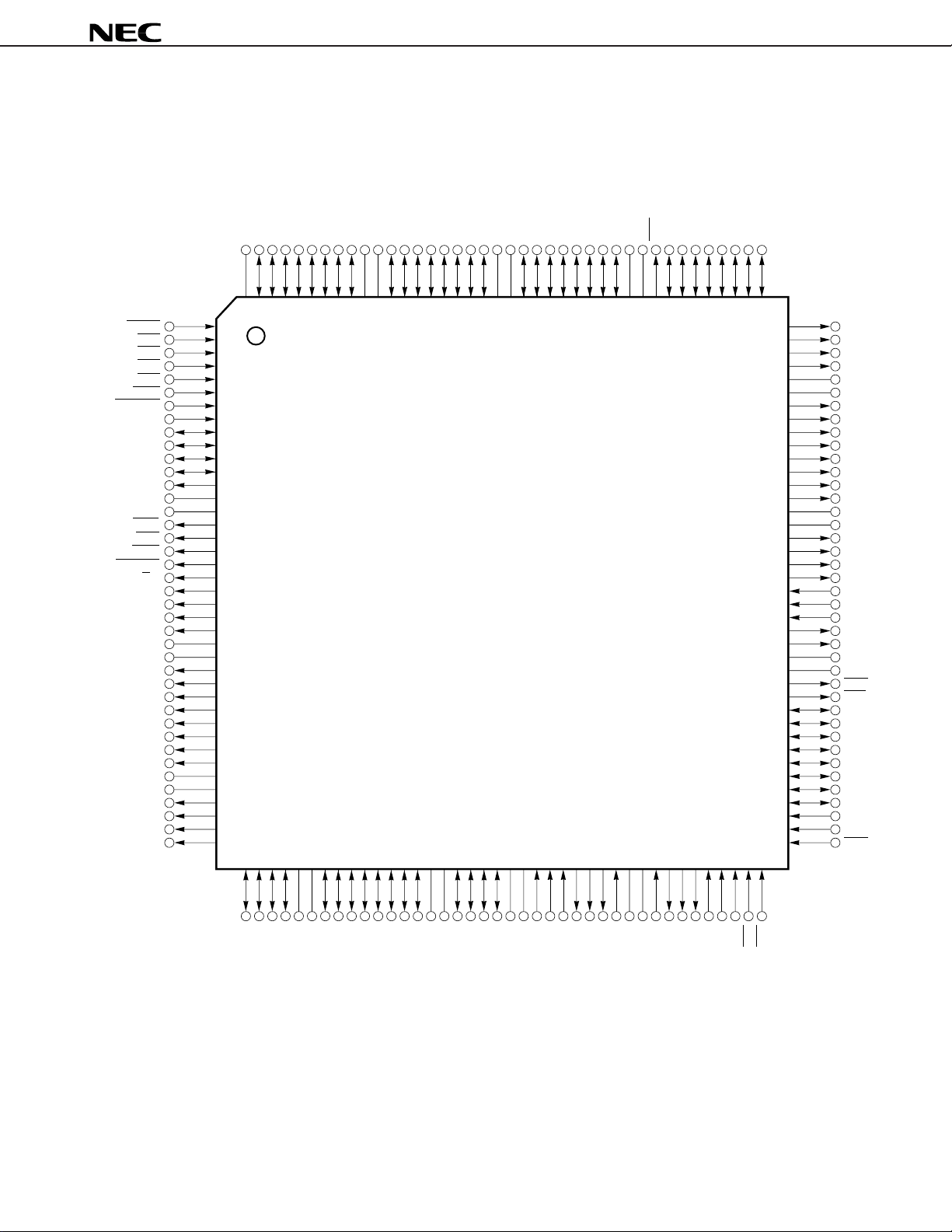
PIN CONFIGURATION
µ
PD77016GM-KMD
160-pin plastic QFP (FINE PITCH) (24 × 24 mm) (Top View)
µ
PD77016
RESET
INT4
INT3
INT2
INT1
WAIT
HOLDRQ
CLKIN
P3
P2
P1
P0
CLKOUT
GND
V
MWR
MRD
BSTB
HOLDAK
X/Y
DA15
DA14
DA13
DA12
GND
V
DA11
DA10
DA9
DA8
DA7
DA6
DA5
DA4
GND
V
DA3
DA2
DA1
DA0
NC
ID0
ID1
ID2
ID3
ID4
ID5
ID6
ID7
VDDGND
ID8
ID9
ID10
ID11
ID12
ID13
ID14
ID15
VDDGND
ID16
ID17
ID18
ID19
ID20
ID21
ID22
ID23
DD
PWR
ID24
GND
V
ID25
ID26
ID27
ID28
ID29
ID30
ID31
121122123124125126127128129130131132133134135136137138139140141142143144145146147148149150151152153154155156157158159160
1
2
3
4
5
6
7
8
9
10
11
12
13
14
DD
15
16
17
18
19
20
21
22
23
24
25
DD
26
27
28
29
30
31
32
33
34
35
DD
36
37
38
39
40
120
119
118
117
116
115
114
113
112
111
110
109
108
107
106
105
104
103
102
101
100
99
98
97
96
95
94
93
92
91
90
89
88
87
86
85
84
83
82
81
IA0
IA1
IA2
IA3
V
DD
GND
IA4
IA5
IA6
IA7
IA8
IA9
IA10
IA11
DD
V
GND
IA12
IA13
IA14
IA15
TMS
TDI
TCK
TIC
TDO
DD
V
GND
HWE
HRE
HD0
HD1
HD2
HD3
HD4
HD5
HD6
HD7
HA1
HA0
HWR
80797877767574737271706968676665646362616059585756555453525150494847464544434241
D15
D14
D13
D12
GND
DD
V
D11
D9D8D7D6D5
D10
D4
GND
DD
D3D2D1
V
D0
GND
DD
V
SI1
SCK1
SIEN1
SO1
SIAK1
GND
SOEN1
SORQ1
DD
V
SOEN2
SORQ2
SO2
SCK2
SIAK2
SI2
SIEN2
HCS
HRD
5

PIN IDENTIFICATION
BSTB: Bus Strobe
CLKIN: Clock Input
CLKOUT: Clock Output
D0-D15: 16 Bits Data Bus
DA0-DA15: External Data Memory Address Bus
GND: Ground
HA0,HA1: Host Data Access
HCS: Host Chip Select
HD0-HD7: Host Data Bus
HOLDAK: Hold Acknowledge
HOLDRQ: Hold Request
HRD: Host Read
HRE: Host Read Enable
HWE: Host Write Enable
HWR: Host Write
IA0-IA15: Instruction Memory Address Output
ID0-ID31: Instruction Data Input
INT1-INT4: Interrupt
MRD: Memory Read Output
MWR: Memory Write Output
N.C: No Connection
P0-P3: Port
PWR: Program Memory Write Strobe
RESET: Reset
SCK1,SCK2: Serial Clock Input
SI1,SI2: Serial Data Input
SIAK1,SIAK2: Serial Input Acknowledge
SIEN1,SIEN2: Serial Input Enable
SO1,SO2: Serial Data Output
SOEN1,SOEN2: Serial Output Enable
SORQ1,SORQ2: Serial Output Request
TCK: Test Clock Input
TDI: Test Data Input
TDO: Test Data Output
TICE: Test In-Circuit Emulator
TMS: Test Mode Select
DD: Power Supply
V
WAIT: Wait Input
X/Y: X/Y Memory Select
µ
PD77016
6
µ
PD77016
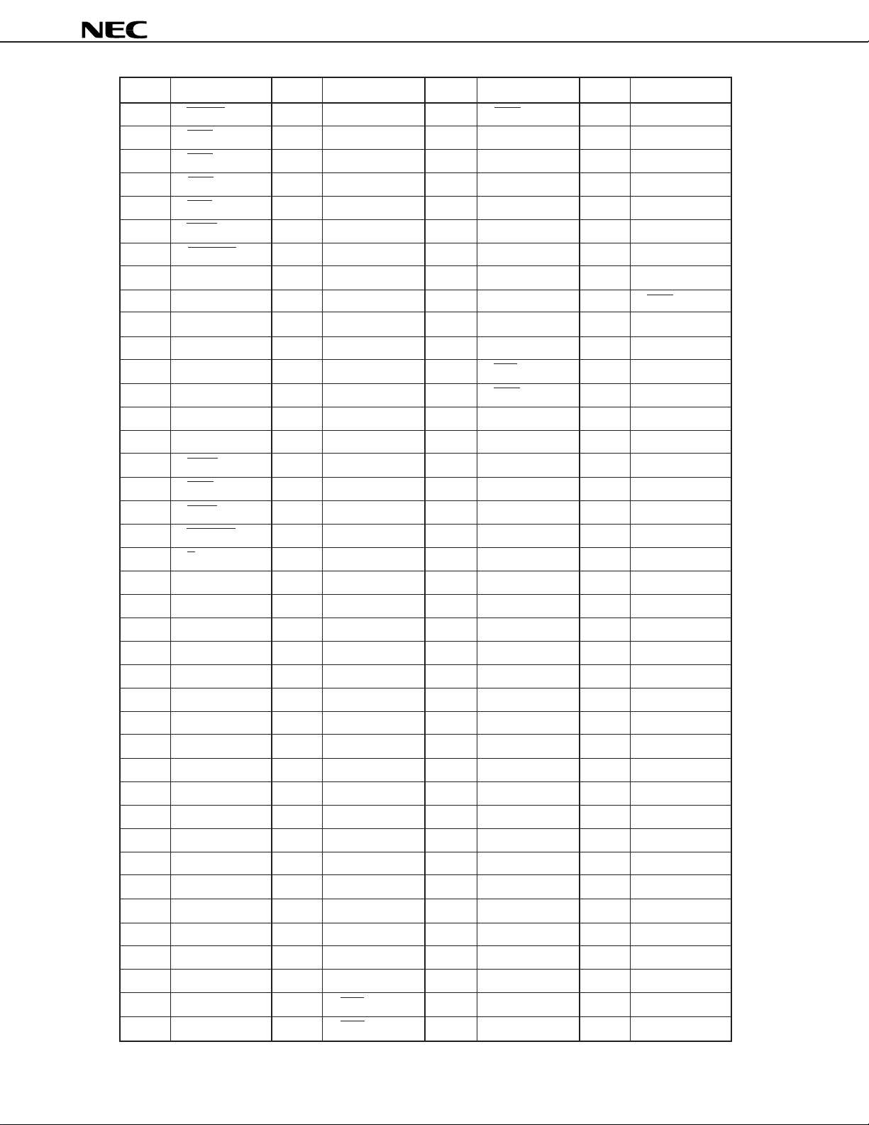
Pin No. Symbol
1 RESET
2 INT4
3 INT3
4 INT2
5 INT1
6 WAIT
7 HOLDRQ
8 CLKIN
9P3
10 P2
11 P1
12 P0
13 CLKOUT
14 GND
15 VDD
16 MWR
17 MRD
18 BSTB
19 HOLDAK
20 X/Y
21 DA15
22 DA14
23 DA13
24 DA12
25 GND
26 VDD
27 DA11
28 DA10
29 DA9
30 DA8
31 DA7
32 DA6
33 DA5
34 DA4
35 GND
36 VDD
37 DA3
38 DA2
39 DA1
40 DA0
Pin No. Symbol
41 D15
42 D14
43 D13
44 D12
45 GND
46 VDD
47 D11
48 D10
49 D9
50 D8
51 D7
52 D6
53 D5
54 D4
55 GND
56 VDD
57 D3
58 D2
59 D1
60 D0
61 GND
62 VDD
63 SI1
64 SIEN1
65 SCK1
66 SIAK1
67 SO1
68 SORQ1
69 SOEN1
70 GND
71 VDD
72 SOEN2
73 SORQ2
74 SO2
75 SIAK2
76 SCK2
77 SIEN2
78 SI2
79 HCS
80 HRD
Pin No. Symbol
81 HWR
82 HA0
83 HA1
84 HD7
85 HD6
86 HD5
87 HD4
88 HD3
89 HD2
90 HD1
91 HD0
92 HRE
93 HWE
94 GND
95 VDD
96 TDO
97 TICE
98 TCK
99 TDI
100 TMS
101 IA15
102 IA14
103 IA13
104 IA12
105 GND
106 VDD
107 IA11
108 IA10
109 IA9
110 IA8
111 IA7
112 IA6
113 IA5
114 IA4
115 GND
116 VDD
117 IA3
118 IA2
119 IA1
120 IA0
Pin No. Symbol
121 ID31
122 ID30
123 ID29
124 ID28
125 ID27
126 ID26
127 ID25
128 ID24
129 PWR
130 GND
131 VDD
132 ID23
133 ID22
134 ID21
135 ID20
136 ID19
137 ID18
138 ID17
139 ID16
140 GND
141 VDD
142 ID15
143 ID14
144 ID13
145 ID12
146 ID11
147 ID10
148 ID9
149 ID8
150 GND
151 VDD
152 ID7
153 ID6
154 ID5
155 ID4
156 ID3
157 ID2
158 ID1
159 ID0
160 NC
7

µ
PD77016
CONTENTS
1. PIN FUNCTIONS............................................................................................................................... 9
1.1 Pin Functions........................................................................................................................................... 9
1.2 Recommended Connection for Unused Pins .......................................................................................14
2. FUNCTIONS...................................................................................................................................... 15
2.1 Pipeline Processing ................................................................................................................................ 15
2.1.1 Outline........................................................................................................................................... 15
2.1.2 Instructions with Delay .................................................................................................................. 15
2.2 Program Control Unit.............................................................................................................................. 16
2.3 Operation Unit ......................................................................................................................................... 16
2.3.1 General register (R0 to R7)........................................................................................................... 16
2.3.2 MAC: Multiply ACcumulator ......................................................................................................... 17
2.3.3 ALU: Arithmetic Logic Unit ........................................................................................................... 17
2.3.4 BSFT: Barrel ShiFTer................................................................................................................... 17
2.3.5 SAC: Shifter And Count Circuit .................................................................................................... 17
2.3.6 CJC: Condition Judge Circuit ....................................................................................................... 17
2.4 Memory..................................................................................................................................................... 18
2.4.1 Instruction RAM Outline ................................................................................................................ 19
2.4.2 Data Memory Outline .................................................................................................................... 19
2.4.3 Data Memory Addressing.............................................................................................................. 19
2.5 On-chip Peripheral Circuit...................................................................................................................... 20
2.5.1 Serial Interface Outline.................................................................................................................. 20
2.5.2 Host Interface Outline.................................................................................................................... 20
2.5.3 General Input/output Ports Outline................................................................................................ 20
2.5.4 Wait Cycle Register....................................................................................................................... 20
3. INSTRUCTIONS................................................................................................................................ 21
3.1 Outline...................................................................................................................................................... 21
3.2 Instruction Set and Operation................................................................................................................ 22
4. ELECTRICAL SPECIFICATIONS.....................................................................................................29
5. PACKAGE DRAWING ...................................................................................................................... 50
6. RECOMMENDED SOLDERING CONDITIONS................................................................................ 51
8

1. PIN FUNCTIONS
1.1 Pin Functions
• Power supply
Symbol Pin No. I/O Function
µ
PD77016
VDD – +5V power supply
GND – Ground
15, 26, 36, 46, 56, 62, 71,
95, 106, 116, 131, 141, 151
14, 25, 35, 45, 55, 61, 70,
94, 105, 115, 130, 140, 150
• System control
Symbol Pin No. I/O Function
CLKIN 8 I External clock input
CLKOUT 13 O Internal system clock output
RESET 1 I Internal system reset signal input
• Interrupt
Symbol Pin No. I/O Function
INT4 - INT1 2, 3, 4, 5 I Maskable external interrupt input
• Falling edge detection
9

• External data memory interface
Symbol Pin No. I/O Function
X/Y 20 O Memory select signal output
(3S) • 0: X memory is used.
• 1: Y memory is used.
DA15 - DA0 Note 1. O Address bus to external data memory
(3S) • External data memory is accessed.
• During the external memory is not accessed, these pins
keep the previous level.
These pins are set to low level; 0x0000, by reset.
They continue outputting low level until the first external
memory access.
D15 - D0 Note 2. I/O 16 bits data bus to external data memory
(3S) • External data memory is accessed.
MRD 17 O Read output
(3S) • Reads external memory
µ
PD77016
MWR 16 O Write output
(3S) • Writes external memory
WAIT 6 I Wait signal input
• Wait cycle is input when external memory is read.
1: No wait
0: Wait
HOLDRQ 7 I Hold request signal input
• Input low level when external data memory bus is
expected to use.
BSTB 18 O Bus strobe signal output
• Outputs low level while the µPD77016 is occupying
external memory bus.
HOLDAK 19 O Hold acknowledge signal output
• Outputs low level when the µPD77016 permits external
device to use external data memory bus.
Note 1. DA15 to DA0 pins are located on Pin No. 21 - 24, 27 - 34, 37 - 40.
2. D15 to D0 pins are located on Pin No. 41 - 44, 47 - 54, 57 - 60.
Remark The state of the pins added 3S becomes high impedance when the external memory is not accessed or bus release signal
(HOLDAK = 0) is output.
10

• Serial interface
Symbol Pin No. I/O Function
SCK1 65 I Clock input for serial 1
SORQ1 68 O Serial output 1 request
SOEN1 69 I Serial output 1 enable
SO1 67 O (3S) Serial data output 1
SIEN1 64 I Serial input 1 enable
SI1 63 I Serial data input 1
SCK2 76 I Clock input for serial 2
SORQ2 73 O Serial output 2 request
SOEN2 72 I Serial output 2 enable
µ
PD77016
SO2 74 O (3S) Serial data output 2
SIEN2 77 I Serial input 2 enable
SI2 78 I Serial data input 2
SIAK1 66 O Serial input 1 acknowledge
SIAK2 75 O Serial input 2 acknowledge
Remark The state of the pins added 3S becomes high impedance, when data output have been finished or RESET is input.
11

• Host interface
Symbol Pin No. I/O Function
HA1 83 I Specifies register which HD7 to HD0 access
1: Accesses HST: Host interface status register
when HA1 = 0
0: Accesses HDT(out): Host transmit data register when
HRD = 0
0: Accesses HDT(in): Host receive data register when
HWR = 0
HA0 82 I Specifies bits of registers which HD7 to HD0 access
• 1: Accesses bits 15-8 of HST, HDT (out), HDT (in)
• 0: Accesses bits 7-0 of HST, HDT (out), HDT (in)
HCS 79 I Chip select input
HRD 80 I Host read input
HWR 81 I Host write input
µ
PD77016
HRE 92 O Host read enable output
HWE 93 O Host write enable output
HD7 - HD0 84 - 91 I/O (3S) 8 bits host data bus
Remark The state of the pins added 3S becomes high impedance when the host does not access host interface.
• I/O port
Symbol Pin No. I/O Function
P3 - P0 9 - 12 I/O I/O port
12

• External instructions memory interface
Symbol Pin No. I/O Function
IA15 - IA0 Note 1. O (3S) Address bus to external instruction memory
• Even the internal instruction memory is accessed, the
address is output to the external instruction memory.
In this case, the µPD77016 ignores data of external
instruction memory output.
ID31 - ID0 Note 2. I/O (3S) 32 bits instruction input
PWR 129 O (3S) Program memory write strobe
• Write strobe for external instruction memory. This pin
loads program to external instruction memory (not
internal memory) while µPD77016 is in boot operation.
Note 1. IA15 to IA0 pins are located on these pins: 101 to 104, 107 to 114, 117 to 120
2. ID31 to ID0 pins are located on these pins: 121 to 128, 132 to 139, 142 to 149, 152 to 159
Remark The state of the pins added 3S becomes high impedance when RESET is input.
µ
PD77016
• Debugging interface
Symbol Pin No. I/O Function
TDO 96 O For debugging
TICE 97 O For debugging
TCK 98 I For debugging
TDI 99 I For debugging
TMS 100 I For debugging
13
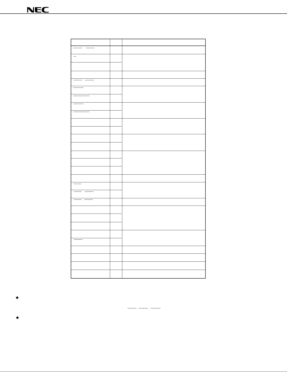
1.2 Recommended Connection for Unused Pins
µ
PD77016
Pin I/O
INT1 - INT4 I
X/Y O
DA0 - DA15 O
D0 - D15
MRD, MWR O
WAIT I
HOLDRQ I
BSTB O
HOLDAK O
SCK1, SCK2 I
SI1, SI2 I
SOEN1, SOEN2 I
SIEN1, SIEN2 I
SORQ1, SORQ2 O
SO1, SO2 O
SIAK1, SIAK2 O
HA0, HA1 I
HCS I
HRD, HWR I
Note 1
I/O
Recommended connection
connect to VDD
open
connect to VDD or GND, via a resistor
open
connect to VDD
open
connect to VDD or GND
connect to GND
open
connect to VDD or GND
connect to VDD
HRE, HWE O
HD0 - HD7
P0 - P3 I/O
ID0 - ID31 I/O
IA0 - IA15 O
PWR O
TCK I
TDO, TICE O
TMS, TDI I
CLKOUT O
Note 2
open
I/O
connect to VDD or GND, via a resistor
open
connect to GND, via a resistor
open
open(pull-up internally)
open
Notes 1. Can leave open, if no access to external data memory is
executed in the whole of program.
But in the HALT mode when the current consumption is
reduced, connect a pin as recommended connection.
2. Can leave open, if HCS, HRD, HWR are fixed to high level.
But in the HALT mode when the current consumption is
reduced, connect a pin as recommended connection.
Remark I: Input pin, O: Output pin, I/O: Input/Output pin
14

µ
PD77016
2. FUNCTIONS
2.1 Pipeline Processing
This section describes the µPD77016 pipeline processing.
2.1.1 Outline
µ
PD77016 basic operations are executed in following 3-stage pipeline.
The
(1) instruction fetch; if
(2) Instruction decoding; id
(3) execution; ex
µ
When the
with written back to general registers. Pipeline processing actualizes programming without delay time to execute
instructions and write back data. Three successive instructions and their processing timing are shown below.
PD77016 operates a result of a instruction just executed before, the data is input to ALU in parallel
Pipeline Processing Timing
if1 id1 ex1
if2 id2 ex2
if3 id3 ex3
1 instruction cycle
2.1.2 Instructions with Delay
The following instructions have delay time in execution.
(1) Instructions to control interrupt
2 instruction cycles have been taken between instruction fetch and execution.
(2) Inter-register transfer instructions and immediate data set instructions
When data is set in data pointer, it needs 2 instruction cycles before the data is valid.
15
µ
PD77016
2.2 Program Control Unit
Program control unit controls not only count up of program counter in normal operation, but loop, repeat,
branch, halt and interrupt.
In addition to loop stack of loop 4 level and program stack of 15 level, software stack can be used for multi-
loop and multi-interrupt/subroutine call.
µ
PD77016 has external 4 interruptions and internal 6 interruptions from peripheral, and specifies interrupt
The
enable or disable independently.
The HALT instruction causes the µPD77016 to place in low power standby mode.
When the HALT instruction is executed, power consumption decreases. HALT mode is released by interrupt
input or hardware reset input. It takes several system clock to recover.
2.3 Operation Unit
Operation unit consists of the following five parts.
– 40 bits general register × 8 for data load/store and input/output of operation data
– 16 bits × 16 bits + 40 bits → 40 bits multiply accumulator
– 40 bits Data ALU
– 40 bits barrel shifter
– SAC: shifter and count circuit.
Standard word length is 40 bits to make overflow check and adjustment easy, and to accumulate the result
of 16 bits × 16 bits multiplication correctly.
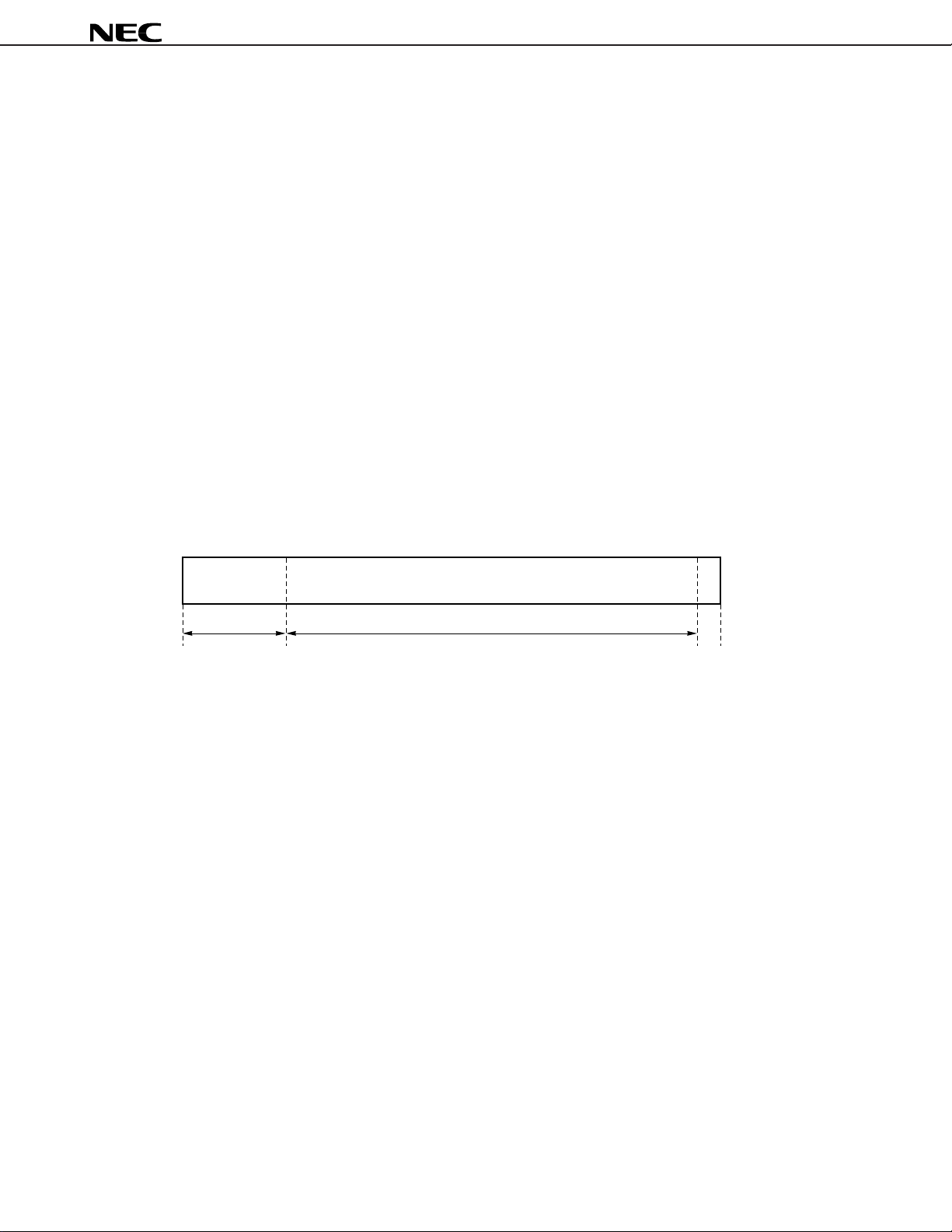
SSSSSSSS
Head room
2.3.1 General register (R0 to R7)
µ
PD77016 has eight 40 bits registers for operation input/output and load/store with memory. General
The
register consists of the following three parts.
– R0L to R7L (bit 15 to bit 0)
– R0H to R7H (bit 31 to bit 16)
– R0E to R7E (bit 39 to bit 32)
But each of RnL, RnH and RnE are treated as a register in the following conditions.
(1) General register used as 40 bits register
General registers are treated as 40 bits register, when they are used for the following aims.
(a) Operand for triminal operation (except for multiplier input)
(b) Operand for dyadic operation (except for multiplier and shift value)
(c) Operand for monadic operation (except for exponent instructions)
(d) Operand for operation
(e) Operand for conditional judge
(f) Destination for load instruction (with sign extension and 0 clear)
Result of multiplication among two's complement data
0
1313239
0
(2) General register used as 32 bits register
Bit 31 to bit 0 of general register are treated as 32 bits register, when it is used for a operand of exponent
instruction.
16

µ
PD77016
(3) General register used as 24 bits register
Bit 39 to bit 16 of general register are treated as 24 bits register, when it is used for destination with extended
sign for a load/store instruction.
(4) General register used as 16 bits register
Bit 31 to bit 16 of general register are treated as 16 bits register, when it is used for the following aims.
(a) Signed operand for multiplier
(b) Source/destination for load/store instruction
Bit 15 to bit 0 of general register are treated as 16 bits register, when it is used for the following aims.
(c) Unsigned operand for multiplier
(d) Shift value for shift instruction
(e) Source/destination for load/store instruction
(f) Source/destination for inter-register transfer instruction
(g) Destination for immediate data set instruction
(f) Hardware loop times
(5) General register used as 8 bits register
Bit 39 to bit 32 of general register are treated as 8 bits register, when it is used for source/destination of load/
store instruction.
2.3.2 MAC: Multiply ACcumulator
MAC multiplies a pair of 16 bits data, and adds or subtract the result and 40 bits data. MAC outputs 40 bits
data.
MAC operates three types of multiplication: signed data × signed data, signed data × unsigned data and
unsigned data × unsigned data.
Result of multiplication and 40 bits data for addition can be added after 1 or 16 bits arithmetic shift right.
2.3.3 ALU: Arithmetic Logic Unit
ALU performs arithmetic operation and logic operation. Both input/output data are 40 bits.
2.3.4 BSFT: Barrel ShiFTer
BSFT performs shift right/left operation. Both input/output data are 40 bits. There are two types of shift right
operations; arithmetic shift right which sign is extended, and logic shift right which is input 0 in MSB first.
2.3.5 SAC: Shifter And Count Circuit
SAC calculates and outputs shift value for normalization. SAC is input 32 bits data and outputs the 40 bits
data. Then, bit 39 to bit 5 of output data is always 0.
2.3.6 CJC: Condition Judge Circuit
CJC judges whether condition is true or false with 40 bits input data. A conditional instruction is executed
when the result is true, and not executed when the result is false.
17
 Loading...