
DATA SHEET
MOS INTEGRATED CIRCUIT
µ
PD75P3036
4-BIT SINGLE-CHIP MICROCONTROLLER
The µPD75P3036 replaces the µPD753036’s internal mask ROM with a one-time PROM or EPROM.
µ
Because the
development using the
PD75P3036 supports programming by users, it is suitable for use in prototype testing for system
µ
PD753036 and for use in small-scale production.
*
Caution The
Detailed descriptions of functions are provided in the following document. Be sure to read the document
before designing.
FEATURES
• Compatible with
µ
PD75P3036KK-T is not designed to guarantee the reliability required for use in mass-
production. Please use it only for performance evaluation during testing and test production runs.
µ
PD753036 User’s Manual : U10201E
µ
PD753036
• Internal PROM: 16384 × 8 bits
µ
PD75P3036KK-T : Reprogrammable (ideally suited for system evaluation)
•
µ
PD75P3036GC, 75P3036GK : One-time programmable (ideally suited for small-scale production)
•
• Internal RAM: 768 × 4 bits
• Can operate in the same power supply voltage as the mask version
DD = 1.8 to 5.5 V
•V
µ
PD753036
• LCD controller/driver
• A/D converter
Caution Mask-option pull-up resistors are not provided in this device.
ORDERING INFORMATION
Part Number Package Internal PROM Quality Grade
µ
PD75P3036GC-3B9 80-pin plastic QFP One-time PROM Standard
µ
PD75P3036GK-BE9 80-pin plastic TQFP One-time PROM Standard
µ
PD75P3036KK-T 80-pin ceramic WQFN EPROM Not applicable
*
Please refer to "Quality Grades on NEC Semiconductor Devices" (Document No. C11531E) published by
NEC Corporation to know the specification of quality grade on the devices and its recommended applications.
In this document, the term PROM is used in parts common to one-time PROM versions and EPROM versions.
The information in this document is subject to change without notice.
Document No. U11575EJ1V0DS00 (1st edition)
(Previous No. IP-3657)
Date Published November 1996 P
Printed in Japan
(14 × 14 mm, 0.65-mm pitch)
(fine pitch) (12 × 12 mm, 0.5-mm pitch)
The mark shows major revised points.
*
©
1996

Functional Outline
Parameter Function
Instruction execution time • 0.95, 1.91, 3.81, 15.3 µs (main system clock: during 4.19-MHz operation)
• 0.67, 1.33, 2.67, 10.7 µs (main system clock: during 6.0-MHz operation)
• 122 µs (subsystem clock: during 32.768-kHz operation)
Internal memory PROM 16384 × 8 bits
RAM 768 × 4 bits
General purpose register • 4-bit operation: 8 × 4 banks
• 8-bit operation: 4 × 4 banks
Input/ CMOS input 8 On-chip pull-up resistors can be specified by using software: 27
output
port
*
LCD controller/driver • Segment selection: 12/16/20 segments (can be changed to bit port output
Timer 5 channels
Serial interface • 3-wire serial I/O mode ... MSB or LSB can be selected for transferring first bit
A/D converter 8-bit resolution: 8 channels
Bit sequential buffer (BSB) 16 bits
Clock output (PCL) • Φ, 524, 262, 65.5 kHz (main system clock: during 4.19-MHz operation)
Buzzer output (BUZ) • 2, 4, 32 kHz (main system clock: during 4.19-MHz operation
Vectored interrupt External: 3, Internal: 5
Test input External: 1, Internal: 1
System clock oscillator • Ceramic or crystal oscillator for main system clock oscillation
Standby function STOP/HALT mode
Power supply voltage VDD = 1.8 to 5.5 V
Package • 80-pin plastic QFP (14 × 14 mm)
CMOS input/output 20
Bit port output 8 Also used for segment pins
N-ch open-drain 8 13 V withstand voltage
input/output pins
Total 44
in unit of 4; max. 8)
• Display mode selection: Static, 1/2 duty (1/2 bias), 1/3 duty (1/2 bias),
1/3 duty (1/3 bias), 1/4 duty (1/3 bias)
• 8-bit timer/event counter: 3 channels
(16-bit timer/event counter, carrier generator, timer with gate)
• Basic interval/watchdog timer: 1 channel
• Watch timer: 1 channel
• 2-wire serial I/O mode
• SBI mode
• Φ, 750, 375, 93.8 kHz (main system clock: during 6.0-MHz operation)
or subsystem clock: during 32.768-kHz operation)
• 2.86, 5.72, 45.8 kHz (main system clock: during 6.0-MHz operation)
• Crystal oscillator for subsystem clock oscillation
• 80-pin plastic TQFP (fine pitch) (12 × 12 mm)
• 80-pin ceramic WQFN
*
µ
PD75P3036
2

µ
PD75P3036
CONTENTS
1. PIN CONFIGURATION (Top View) ............................................................................................... 4
2. BLOCK DIAGRAM ......................................................................................................................... 6
3. PIN FUNCTIONS ............................................................................................................................ 7
3.1 Port Pins ................................................................................................................................................ 7
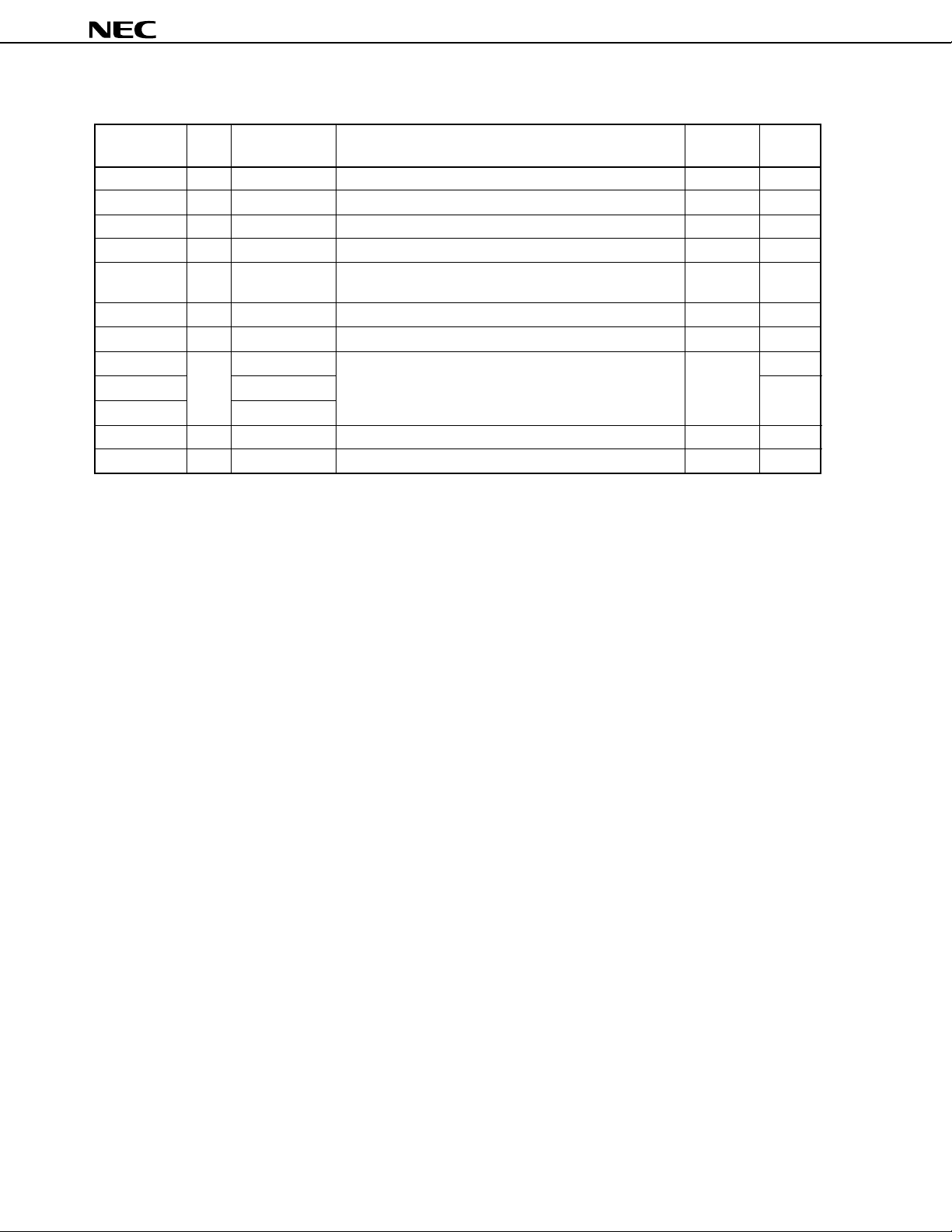
3.2 Non-port Pins ........................................................................................................................................ 9
3.3 Pin Input/Output Circuits......................................................................................................................11
3.4 Recommended Connection of Unused Pins ...................................................................................... 14
4. Mk I MODE AND Mk II MODE SELECTION FUNCTION .............................................................. 15
4.1 Difference between Mk I Mode and Mk II Mode .................................................................................. 15
4.2 Setting of Stack Bank Selection Register (SBS) ................................................................................ 16
5. DIFFERENCES BETWEEN µPD75P3036 AND µPD753036 ........................................................ 17
*
*
*
*
6. PROGRAM COUNTER (PC) AND MEMORY MAP ....................................................................... 18
6.1 Program Counter (PC) .......................................................................................................................... 18
6.2 Program Memory (PROM) .................................................................................................................... 18
6.3 Data Memory (RAM) .............................................................................................................................. 20
7. INSTRUCTION SET ....................................................................................................................... 21
8. PROM (PROGRAM MEMORY) WRITE AND VERIFY .................................................................. 30
8.1 Operation Modes for Program Memory Write/Verify ......................................................................... 30
8.2 Program Memory Write Procedure ...................................................................................................... 31
8.3 Program Memory Read Procedure ...................................................................................................... 32
9. PROGRAM ERASURE (µPD75P3036KK-T ONLY) ...................................................................... 33
10. OPAQUE FILM ON ERASURE WINDOW (µPD75P3036KK-T ONLY)......................................... 33
11. ONE-TIME PROM SCREENING .................................................................................................... 33
12. ELECTRICAL SPECIFICATIONS .................................................................................................. 34
13. CHARACTERISTIC CURVES (FOR REFERENCE ONLY) ........................................................... 49
*
14. PACKAGE DRAWINGS ................................................................................................................. 51
15. RECOMMENDED SOLDERING CONDITIONS ............................................................................. 54
APPENDIX A. FUNCTION LIST OF µPD75336, 753036, AND 75P3036 .......................................... 55
APPENDIX B. DEVELOPMENT TOOLS ............................................................................................ 56
APPENDIX C. RELATED DOCUMENTS ............................................................................................ 60
3
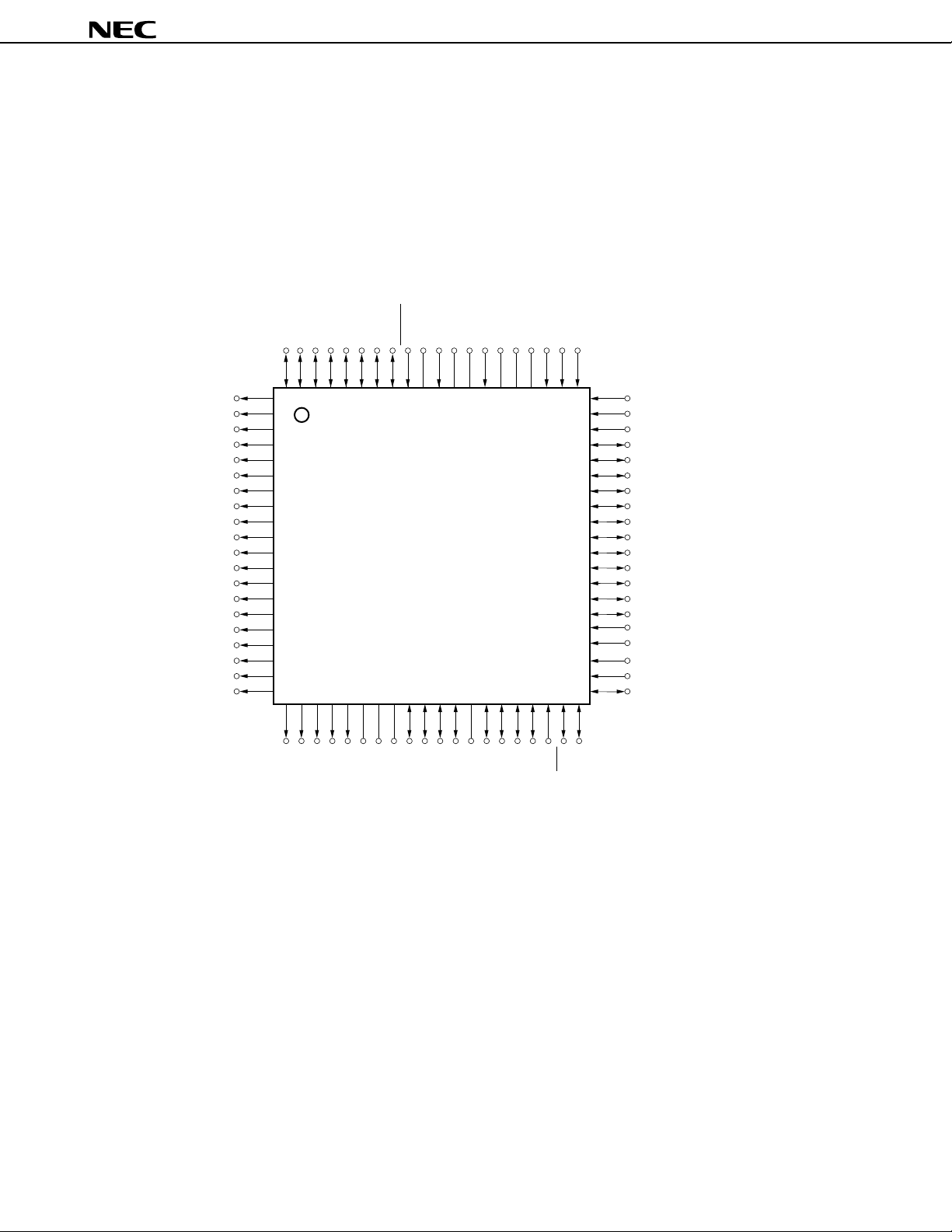
1. PIN CONFIGURATION (Top View)
• 80-pin plastic QFP (14 × 14 mm)
µ
PD75P3036GC-3B9
• 80-pin plastic TQFP (fine pitch) (12 × 12 mm)
µ
PD75P3036GK-BE9
• 80-pin ceramic WQFN
µ
PD75P3036KK-T
P73/KR7
P72/KR6
P71/KR5
P70/KR4
P63/KR3
P62/KR2
P61/KR1
P60/KR0
RESET72X271X170VPP69XT268XT167VDD66AVREF65AVSS64AN563AN462AN3
µ
PD75P3036
S31/BP7
S30/BP6
S29/BP5
S28/BP4
S27/BP3
S26/BP2
S25/BP1
S24/BP0
S23
S22
S21
S20
S19
S18
S17
S16
S15
S14
S13
S12
80
79
78
1
2
3
4
5
6
7
8
9
10
11
12
13
14
15
16
17
18
19
20
77
24
COM021COM122COM223COM3
76
25
75
VLC026VLC127VLC2
BIAS
74
73
28
33
32
VSS
P40/D029P41/D130P42/D231P43/D3
37
38
39
P50/D434P51/D535P52/D636P53/D7
P00/INT4
61
60
59
58
57
56
55
54
53
52
51
50
49
48
47
46
45
44
43
42
41
40
P01/SCK
P02/SO/SB0
AN2
AN1
AN0
P83/AN7
P82/AN6
P81/TI2
P80/TI1
P33/MD3
P32/MD2
P31/SYNC/MD1
P30/LCDCL/MD0
P23/BUZ
P22/PCL/PTO2
P21/PTO1
P20/PTO0
P13/TI0
P12/INT2
P11/INT1
P10/INT0
P03/SI/SB1
Caution Connect the V
4
PP pin directly to VDD.

µ
PD75P3036
PIN IDENTIFICATIONS
P00 to P03 : Port0 S12 to S31 : Segment Output 12-31
P10 to P13 : Port1 COM0 to COM3 : Common Output 0-3
P20 to P23 : Port2 V
P30 to P33 : Port3 BIAS : LCD Power Supply Bias Control
P40 to P43 : Port4 LCDCL : LCD Clock
P50 to P53 : Port5 SYNC : LCD Synchronization
P60 to P63 : Port6 TI0 to TI2 : Timer Input 0-2
P70 to P73 : Port7 PTO0 to PTO2 : Programmable Timer Output 0-2
P80 to P83 : Port8 BUZ : Buzzer Clock
BP0 to BP7 : Bit Port0-7 PCL : Programmable Clock
KR0 to KR7 : Key Return 0-7 INT0, INT1, INT4 : External Vectored Interrupt 0, 1, 4
SCK : Serial Clock INT2 : External Test Input 2
SI : Serial Input X1, X2 : Main System Clock Oscillation 1, 2
SO : Serial Output XT1, XT2 : Subsystem Clock Oscillation 1, 2
SB0, SB1 : Serial Bus 0,1 RESET : Reset
REF : Analog Reference VPP : Programming Power Supply
AV
SS : Analog Ground VDD : Positive Power Supply
AV
AN0-AN7 : Analog Input 0-7 V
MD0 to MD3 : Mode Selection 0-3
D0 to D7 : Data Bus 0-7
LC0 to VLC2 : LCD Power Supply 0-2
SS : Ground
5
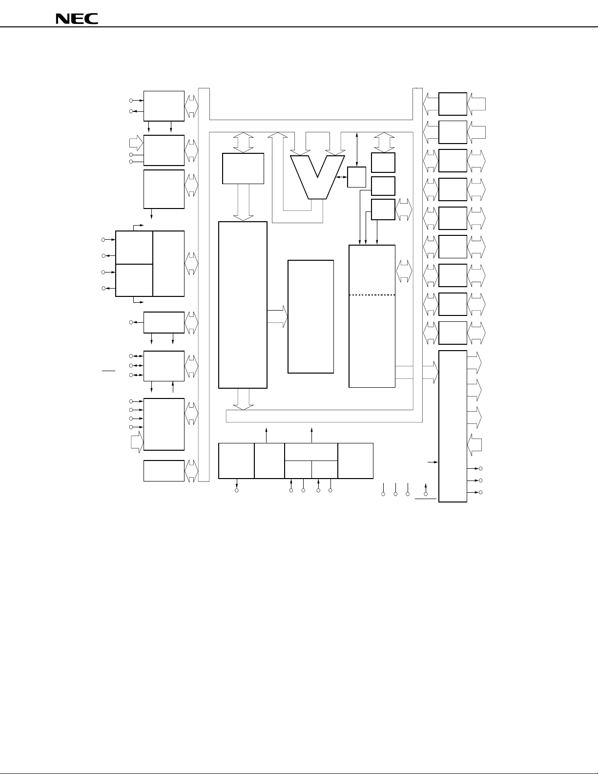
2. BLOCK DIAGRAM
µ
PD75P3036
TI1/P80
PTO1/P21
TI2/P81
PTO2/PCL/P22
SI/SB1/P03
SO/SB0/P02
TI0/P13
PTO0/P20
AN0-AN5
AN6/P82
AN7/P83
AV
REF
AV
SS
8-BIT
TIMER/EVENT
COUNTER #1
8-BIT
TIMER/EVENT
COUNTER #2
BUZ/P23
SCK/P01
INT0/P10
INT1/P11
INT4/P00
INT2/P12
KR0/P60-
KR7/P73
8-BIT
TIMER/EVENT
COUNTER #0
INTT0
8
A/D
CONVERTER
BASIC
INTERVAL
TIMER/
WATCHDOG
TIMER
INTBT
INTT1
CASCADED
16-BIT
TIMER/
EVENT
COUNTER
INTT2
WATCH
TIMER
INTW
CLOCKED
SERIAL
INTERFACE
INTCSI
INTERRUPT
CONTROL
8
BIT SEQ.
BUFFER (16)
TOUT0
f
LCD
TOUT0
PROGRAM
COUNTER
(14)
PROM
PROGRAM
MEMORY
16384 x 8 BITS
CLOCK
OUTPUT
CONTROL
CLOCK
DIVIDER
PCL/P22
DECODE
CONTROL
N
fx/2
SYSTEM CLOCK
GENERATOR
ALU
AND
CPU CLOCK Φ
MAINSUB
X2X1XT2XT1
CY
GENERAL
REG.
RAM
DATA
MEMORY
768 x 4 BITS
STAND BY
CONTROL
SP (8)
SBS
BANK
V
PP
4
4
4
4
4
P00-P03
P10-P13
P20-P23
P30/MD0P33/MD3
P40/D0P43/D3
P50/D4P53/D7
PORT0 4
PORT1
PORT2
PORT3
PORT4
PORT5
PORT6 P60-P634
PORT7 P70-P734
PORT8
P80-P834
S12-S2312
S24/BP0-
8
S31/BP7
LCD
CONTROLLER/
4
COM0COM3
DRIVER
LC0-VLC2
3
V
f
LCD
BIAS
LCDCL/P30
SYNC/P31
V
SS
RESETV
DD
6

3. PIN FUNCTIONS
3.1 Port Pins (1/2)
µ
PD75P3036
Pin name I/O Alternate Function 8-bit Status I/O circuit
function I/O after reset type
P00 Input INT4 This is a 4-bit input port (PORT0). No Input <B>
Connection of an on-chip pull-up resistor can be
P01 I/O SCK specified in 3-bit units by software for P01 to P03. <F>-A
P02 I/O SO/SB0 <F>-B
P03 I/O SI/SB1 <M>-C
P10 Input INT0 This is a 4-bit input port (PORT1). No Input <B>-C
Connection of an on-chip pull-up resistor can be
P11 INT1 specified in 4-bit units by software.
P10/INT0 can select noise elimination circuit.
P12 INT2
P13 TI0
P20 I/O PTO0 This is a 4-bit I/O port (PORT2). No Input E-B
Connection of an on-chip pull-up resistor can be
P21 PTO1 specified in 4-bit units by software.
P22 PCL/PTO2
P23 BUZ
P30 I/O LCDCL/MD0 This is a programmable 4-bit I/O port (PORT3). No Input E-B
Input and output can be specified in bit units.
P31 SYNC/MD1 Connection of an on-chip pull-up resistor can be
specified in 4-bit units by software.
P32 MD2
Note 1
*
*
P33 MD3
Note 2
P40
P41
P42
P43
P50
P51
P52
P53
Note 2
Note 2
Note 2
Note 2
Note 2
Note 2
Note 2
I/O D0 This is an N-ch open-drain 4-bit I/O port (PORT4). Yes High M-E
When set to open-drain, voltage is 13 V. impedance
D1 Also functions as data I/O pin (lower 4 bits)
for program memory (PROM) write/verify.
D2
D3
I/O D4 This is an N-ch open-drain 4-bit I/O port (PORT5). High M-E
When set to open-drain, voltage is 13 V. impedance
D5 Also functions as data I/O pin (upper 4 bits)
for program memory (PROM) write/verify.
D6
D7
Notes 1. Circuit types enclosed in brackets indicate Schmitt trigger input.
2. Low level input leakage current increases when input instructions or bit manipulate instructions are executed.
7
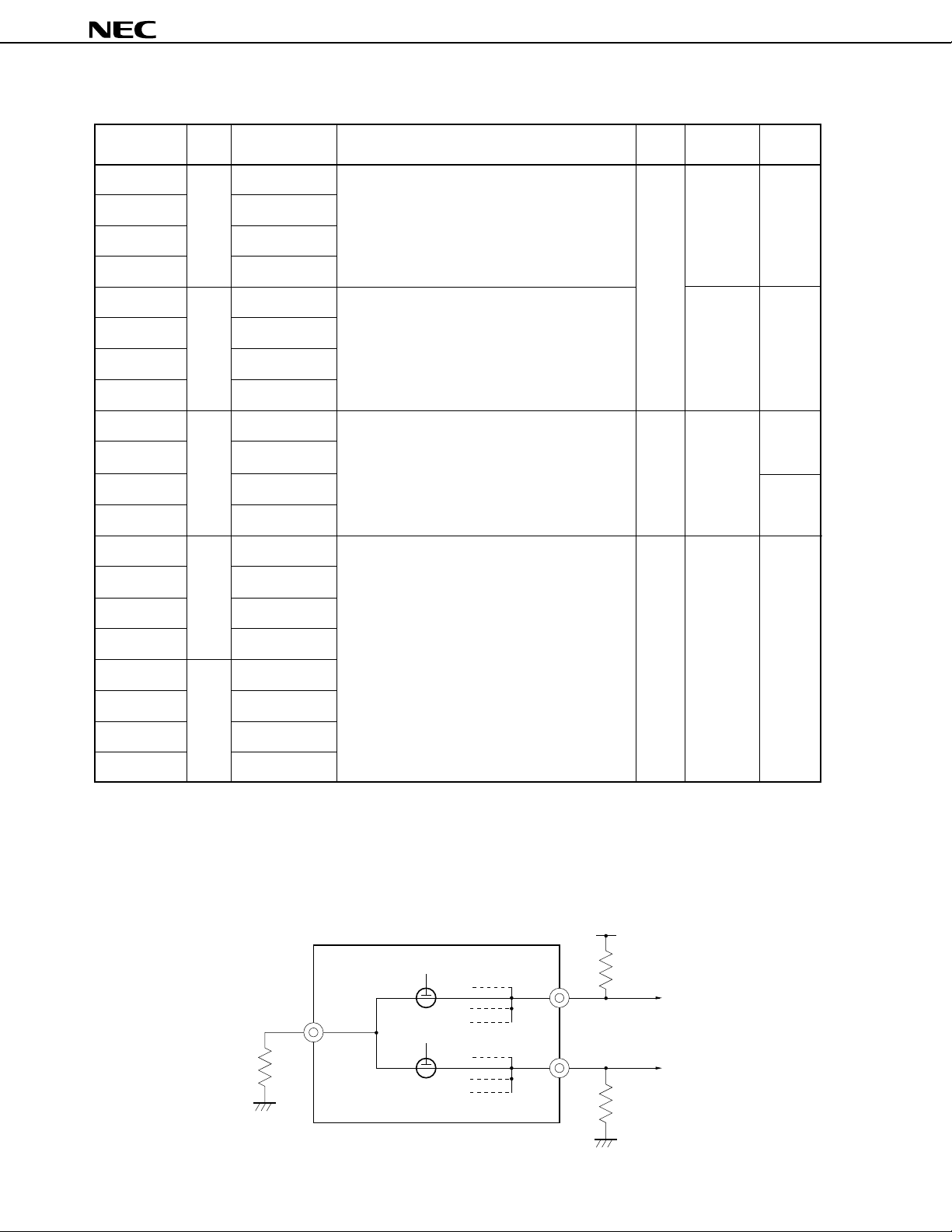
3.1 Port Pins (2/2)
µ
PD75P3036
Pin name I/O Alternate Function 8-bit Status I/O circuit
function I/O after reset type
P60 I/O KR0 This is a programmable 4-bit I/O port (PORT6). Yes Input <F>-A
Input and output can be specified in bit units.
P61 KR1 Connection of an on-chip pull-up resistor can be
specified in 4-bit units by software.
P62 KR2
P63 KR3
P70 I/O KR4 This is a 4-bit I/O port (PORT7). Input <F>-A
Connection of an on-chip pull-up resistor can be
P71 KR5 specified in 4-bit units by software.
P72 KR6
P73 KR7
P80 I/O TI1 This is a 4-bit I/O port (PORT8). No Input <E>-E
Connection of an on-chip pull-up resistor can be
P81 TI2 specified in 4-bit units by software.
P82 AN6 Y-B
P83 AN7
BP0 Output S24 These pins are also used as 1-bit I/O port (BIT No Note 2 H-A
PORT) segment output pin.
BP1 S25
Note 1
BP2 S26
BP3 S27
BP4 Output S28
BP5 S29
BP6 S30
BP7 S31
Notes 1. Circuit types enclosed in brackets indicate Schmitt trigger input.
LC1 as an input source.
*
2. BP0 through BP7 select V
However, the output levels change depending on the external circuit of BP0 through BP7 and V
Example Because BP0 through BP7 are mutually connected inside the
*
BP7 are determined by R
LC1
V
R
1
1, R2, and R3.
PD75P3036
µ
ON
ON
LC1.
µ
PD75P3036, the output levels of BP0 through
V
DD
R
2
BP0
BP1
R
3
8
3.2 Non-port Pins (1/2)
µ
PD75P3036
Pin name I/O Alternate Function Status I/O circuit
function after reset type
TI0 Input P13 External event pulse input to timer/event counter Input <B>-C
TI1 P80 <E>-E
TI2 P81
PTO0 Output P20 Timer/event counter output Input E-B
PTO1 P21
PTO2 P22/PCL
PCL Output P22/PTO2 Clock output Input E-B
BUZ Output P23 Frequency output (for buzzer or system clock trimming) Input E-B
SCK I/O P01 Serial clock I/O Input <F>-A
SO/SB0 I/O P02 Serial data output Input <F>-B
Serial data bus I/O
SI/SB1 I/O P03 Serial data input Input <M>-C
Serial data bus I/O
INT4 Input P00 Edge detection vectored interrupt input Input <B>
(valid for detecting both rising and falling edges)
INT0 Input P10 Edge detection vectored interrupt input Noise elimination Input <B>-C
(detected edge is selectable) circuit
INT0/P10 can select noise elimination /asynchronous
circuit. is selectable
INT1 P11 Asynchronous
INT2 Input P12 Rising edge detection test input Asynchonous Input <B>-C
KR0 to KR3 Input P60 to P63 Parallel falling edge detection test input Input <F>-A
KR4 to KR7 Input P70 to P73 Parallel falling edge detection test input Input <F>-A
X1 Input — Ceramic/crystal oscillation circuit connection for main system — —
clock. If using an external clock, input to X1 and input
X2 — — inverted phase to X2.
XT1 Input — Crystal oscillation circuit connection for subsystem clock. — —
If using an external clock, input to XT1 and input inverted
XT2 — — phase to XT2.
RESET Input — System reset input (low level active) — <B>
MD0 I/O P30/LCDCL Mode selection for program memory (PROM) write/verify Input E-B
MD1 P31/SYNC
MD2, MD3 P32, P33
D0 to D3 I/O P40 to P43 Data bus for program memory (PROM) write/verify Input M-E
D4 to D7 P50 to P53
V
PP — — Programmable power supply voltage for program memory — —
(PROM) write/verify.
For normal operation, connect to VDD.
Apply +12.5 V for PROM write/verify.
V
DD — — Positive power supply — —
VSS — — Ground — —
XT1 can be used as a 1-bit (test) input.
Note
Note Circuit types enclosed in brackets indicate Schmitt trigger input.
9
µ
PD75P3036
3.2 Non-port Pins (2/2)
Pin name I/O Alternate Function Status I/O circuit
function after reset type
S12 to S23 Output — Segment signal output Note 1 G-A
S24 to S31 Output BP0 to BP7 Segment signal output Note 1 H-A
COM0 to COM3
V
LC0 to VLC2 — — Power source for LCD driver — —
BIAS Output — Output for external split resistor cut High —
LCDCL
Note 2
SYNC
AN0 to AN5 Input — Analog signal input for A/D converter Input Y
AN6 P82 Y-B
AN7 P83
AV
REF — — A/D converter reference voltage — Z-N
AV
SS — — A/D converter reference GND potential — Z-N
Output — Common signal output Note 1 G-B
impedance
Note 2
Output P30/MD0 Clock output for driving external expansion driver Input E-B
Output P31/MD1 Clock output for synchronization of external expansion driver Input E-B
Notes 1. The VLCX (X = 0, 1, 2) shown below are selected as the input source for the display outputs.
S12 to S31: V
LC1, COM0 to COM2: VLC2, COM3: VLC0
2. These pins are provided for future system expansion. Currently, only P30 and P31 are used.
10
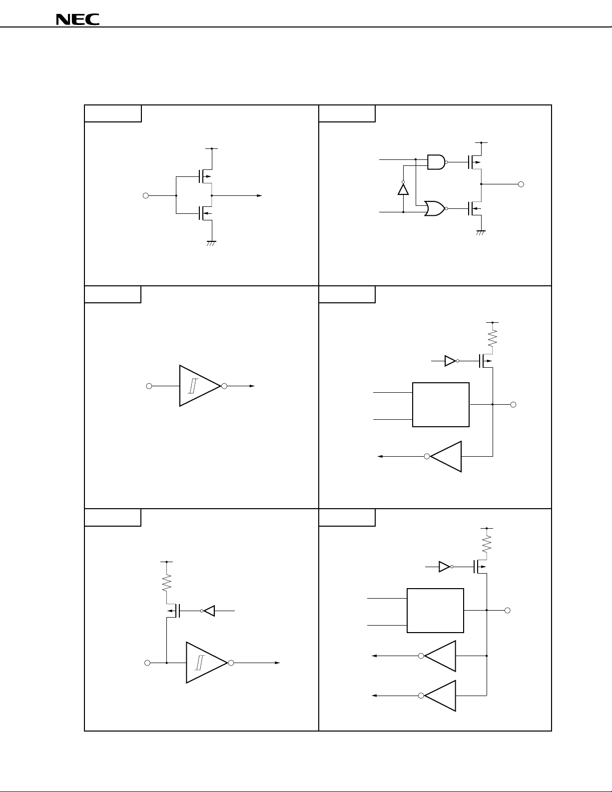
3.3 Pin Input/Output Circuits
µ
The input/output circuits for the
TYPE A TYPE D
PD75P3036’s pins are shown in schematic form below.
µ
PD75P3036
(1/3)
VDD
P-ch
IN
N-ch
CMOS standard input buffer
IN
VDD
data
output
disable
Push-pull output that can be set to output high-impedance
(with both P-ch and N-ch OFF).
TYPE E-BTYPE B
P.U.R.
enable
data
Type D
output
disable
P-ch
N-ch
VDD
P.U.R.
P-ch
IN/OUT
OUT
Schmitt trigger input with hysteresis characteristics.
TYPE B-C TYPE E-E
VDD
P.U.R.
data
output
disable
P-ch
IN
P.U.R. : Pull-Up Resistor
P.U.R.
enable
Type A
P.U.R. : Pull-Up Resistor
P.U.R.
enable
Type D
Type A
Type B
P.U.R. : Pull-Up Resistor
VDD
P.U.R.
P-ch
IN/OUT
11
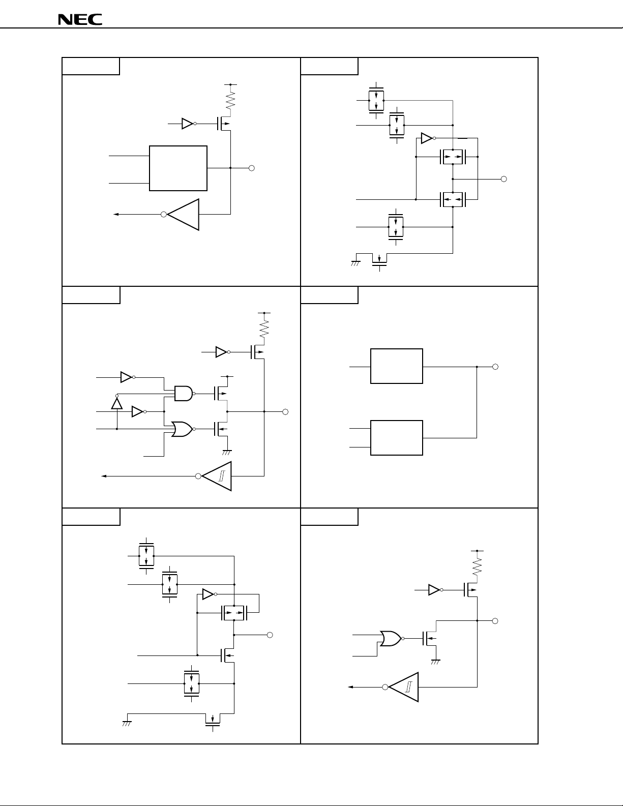
TYPE F-A TYPE G-B
VDD
P.U.R.
µ
PD75P3036
(2/3)
*
V
LC0
output
disable
output
disable
(P)
data
output
disable
data
P.U.R.
enable
Type D
Type B
P.U.R. : Pull-Up Resistor
P.U.R.
enable
output
disable
(N)
VDD
P-ch
P-ch
N-ch
IN/OUT
VDD
P.U.R.
P-ch
IN/OUT
VLC1
COM or SEG
TYPE H-ATYPE F-B
V
SEG
data
Bit Port
data
output
disable
data
LC2
*
N-ch
Type G-A
Type E-B
P-ch
N-ch
N-ch
OUT
P-ch
IN/OUT
P.U.R. : Pull-Up Resistor
TYPE G-A TYPE M-C
*
LC0
V
VLC1
SEG
data
V
LC2
N-chP-ch
OUT
N-ch
N-ch
12
data
output
disable
P.U.R.
enable
N-ch
P.U.R. : Pull-Up Resistor
VDD
P.U.R.
P-ch
IN/OUT
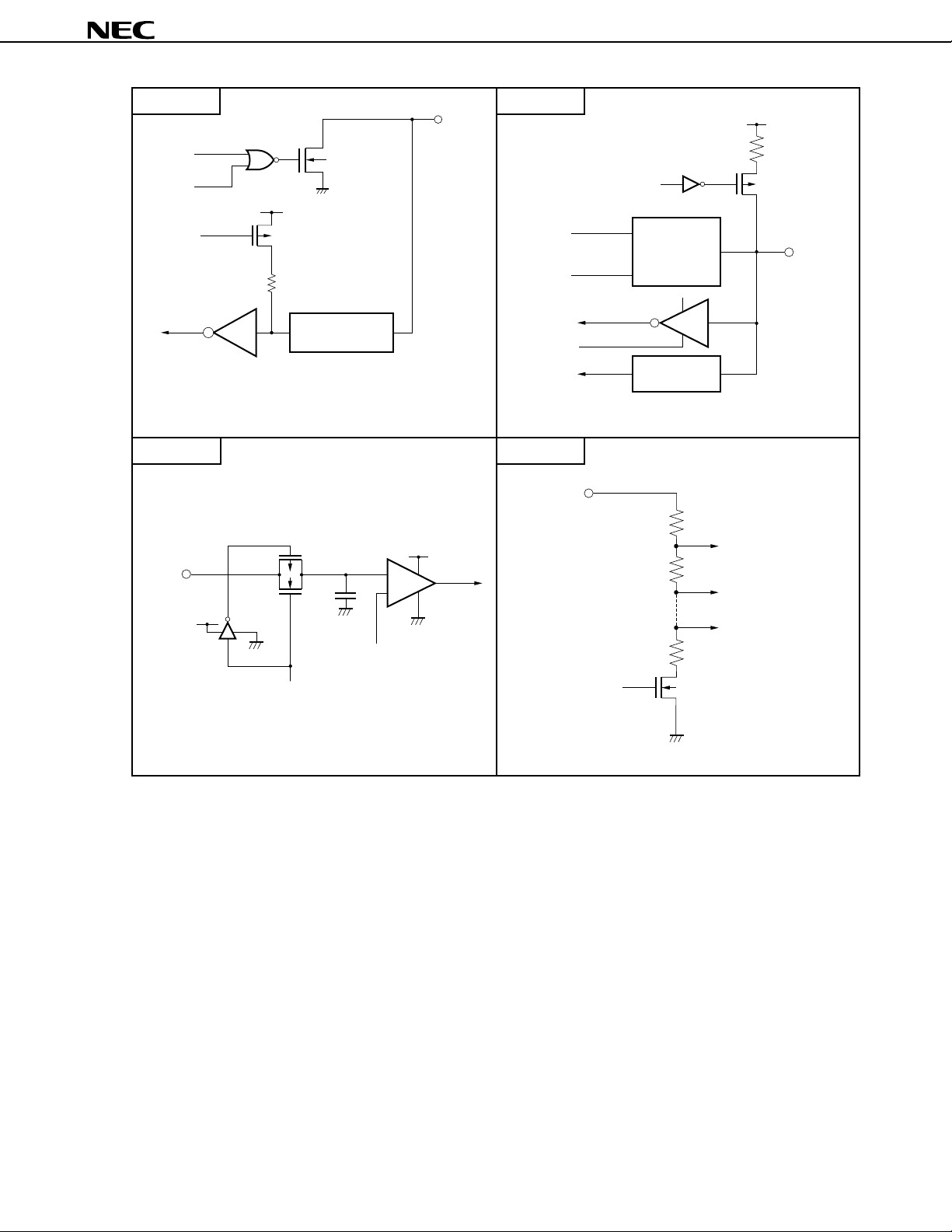
TYPE M-E TYPE Y-B
*
IN/OUT
µ
PD75P3036
VDD
(3/3)
data
output
disable
input
instruction
Note
IN
N-ch
(+13 V
withstand
V
DD
P-ch
P.U.R.
The pull-up resistor operates only when an input
instruction is executed (current flows from V
the pin when the pin is low).
P-ch
N-ch
V
DD
SS
AV
input
enable
voltage)
Note
Voltage limitation
circuit
Sampling C
reference voltage
(from voltage tap of
series resistor string)
(+13 V withstand
voltage)
DD to
VDD
+
–
AVSS
TYPE Z-NTYPE Y
data
output
disable
Note
port
input
P.U.R. : Pull-Up Resistor
*
AVREF
P.U.R.
enable
Type D
Type A
Type Y
N-chADEN
P-ch
IN/OUT
reference
voltage
Note Becomes active when an input instruction is executed.
AVSS
13

3.4 Recommended Connection of Unused Pins
*
Pin Recommended connection
P00/INT4 Connect to VSS or VDD
P01/SCK Connect to VSS or VDD via a resistor individually
P02/SO/SB0
P03/SI/SB1 Connect to V
P10/INT0 to P12/INT2
P13/TI0
P20/PTO0 Input status : connect to V
P21/PTO1 Output status: open
P22/PTO2/PCL
P23/BUZ
P30/LCDCL
P31/SYNC
P32, P33
P40 to P43 Connect to V
P50 to P53
P60/KR0 to P63/KR3
P70/KR4 to P73/KR7
P80/TI1
P81/TI2
P82/AN6
P83/AN7
S12 to S23 Open
S24/BP0 to S31/BP7
COM0 to COM3
V
LC0 to VLC2 Connect to VSS
BIAS Connect to VSS only when VLC0 to VLC2 are all not used.
Note
XT1
Note
XT2
AN0 to AN5 Connect to V
VPP Connect to VDD directly
Connect to VSS or VDD
Input status : connect to VSS or VDD via a resistor individually.
Output status: open
In other cases, leave open.
Connect to VSS or VDD
Open
SS
SS
SS or VDD
SS or VDD via a resistor individually.
µ
PD75P3036
14
Note When the subsystem clock is not used, set SOS.0 to 1 (so as not to use
the internal feedback resistor).

µ
PD75P3036
4. Mk I MODE AND Mk II MODE SELECTION FUNCTION
Setting a stack bank selection (SBS) register for the µPD75P3036 enables the program memory to be switched between
µ
Mk I mode and Mk II mode. This function is applicable when using the
PD75P3036 to evaluate the µPD753036.
When the SBS bit 3 is set to 1 : sets Mk I mode (supports Mk I mode for
When the SBS bit 3 is set to 0 : sets Mk II mode (supports Mk II mode for
4.1 Difference between Mk I Mode and Mk II Mode
Table 4-1 lists points of difference between the Mk I mode and the Mk II mode for the
Table 4-1. Difference between Mk I Mode and Mk II Mode
Item Mk I Mode Mk II Mode
Program counter PC
Program memory (bytes) 16384
Data memory (bits) 768 x 4
Stack Stack bank Selectable via memory banks 0 to 2
No. of stack bytes 2 bytes 3 bytes
Instruction BRA !addr1 instruction Not available Available
CALLA !addr1 instruction
Instruction CALL !addr instruction 3 machine cycles 4 machine cycles
execution time CALLF !faddr instruction 2 machine cycles 3 machine cycles
Supported mask ROM versions When set to Mk I mode for
13-0
µ
µ
PD753036)
µ
PD753036)
µ
PD75P3036.
PD753036 When set to Mk II mode for µPD753036
*
Caution The Mk II mode supports a program area exceeding 16 Kbytes for the 75X and 75XL series.
Therefore, this mode is effective for enhancing software compatibility with products exceeding 16
Kbytes.
When the Mk II mode is selected, the number of stack bytes used during execution of subroutine
call instructions increases by one byte per stack compared to the Mk I mode. When the CALL !addr
and CALLF !faddr instructions are used, the machine cycle becomes longer by one machine cycle.
Therefore, use the Mk I mode if the RAM efficiency and processing performance are more important
than software compatibility.
15
µ
PD75P3036
4.2 Setting of Stack Bank Selection Register (SBS)
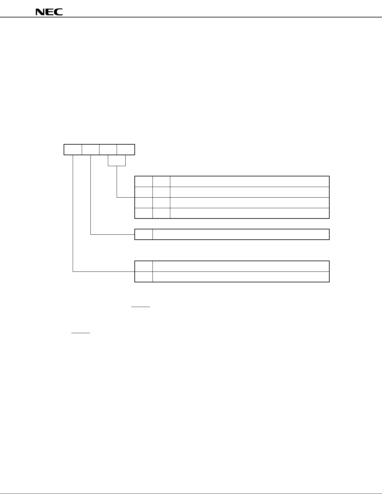
Use the stack bank selection register to switch between Mk I mode and Mk II mode. Figure 4-1 shows the format for doing
this.
The stack bank selection register is set using a 4-bit memory manipulation instruction. When using the Mk I mode, be
Note
sure to initialize the stack bank selection register to 10xxB
Note
be sure to initialize it to 00xxB
.
at the beginning of the program. When using the Mk II mode,
Note Set the desired value for xx.
Figure 4-1. Format of Stack Bank Selection Register
Address 3 2 1 0
SBS3 SBS2 SBS1 SBS0F84H
Symbol
SBS
Stack area specification
0
0
Memory bank 0
0
1
Memory bank 1
1
0
Memory bank 2
1
1
Setting prohibited
0 Be sure to enter “0” for bit 2.
Mode selection specification
01Mk II mode
Mk I mode
Cautions 1. SBS3 is set to “1” after RESET input, and consequently the CPU operates in Mk I mode. When using
instructions for Mk II mode, set SBS3 to “0” and set Mk II mode before using the instructions.
2. When using Mk II mode, execute a subroutine call instruction and an interrupt instruction after
RESET input and after setting the stack bank selection register.
16

µ
PD75P3036
5. DIFFERENCES BETWEEN µPD75P3036 AND µPD753036
The µPD75P3036 replaces the internal mask ROM in the program memory of the µPD753036 with a one-time PROM or
µ
EPROM. The
supports the Mk II mode in the
Table 5-1 lists differences among the
products before using them with PROMs for debugging or prototype testing of application systems or, later, when using
them with a mask ROM for full-scale production.
As to CPU function and on-chip hardware, see the User’s Manual.
PD75P3036’s Mk I mode supports the Mk I mode in the µPD753036 and the µPD75P3036’s Mk II mode
µ
PD753036.
µ
PD75P3036 and the µPD753036. Be sure to check the differences among these
µ
Table 5-1. Differences between
PD75P3036 and µPD753036
Item
Program counter 14 bits
Program memory (bytes) 16384 16384
Mask ROM One-time PROM, EPROM
Data memory (x 4 bits) 768
Mask option Pull-up resistor of Yes (can specify whether to incorporate No (don’t incorporate on-chip)
ports 4, 5 on-chip or not)
Split resistor for LCD
driving power supply
Selection of Yes (can select either 2
oscillation
stabilization wait time
Selection of Yes (can select either use enabled or use No (use enabled)
subsystem clock disabled)
feedback resistor
Pin configuration Pin No. 29 to 32 P40 to P43 P40/D0 to P43/D3
Pin No. 34 to 37 P50 to P53 P50/D4 to P53/D7
Pin No. 50 P30/LCDCL P30/LCDCL/MD0
Pin No. 51 P31/SYNC P31/SYNC/MD1
Pin No. 52 P32 P32/MD2
Pin No. 53 P33 P33/MD3
Pin No. 69 IC V
Other Noise resistance and noise radiation may differ due to the different circuit sizes and mask
layouts.
µ
PD753036
17
/fX or 215/fX)
Note
µ
No (fixed to 215/fX)
PP
PD75P3036
Note
Note 217/fX is 21.8 ms during 6.0-MHz operation, and 31.3 ms during 4.19-MHz operation.
15
/fX is 5.46 ms during 6.0-MHz operation, and 7.81 ms during 4.19-MHz operation.
2
Caution Noise resistance and noise radiation are different in PROM and mask ROM versions. In transferring to
mask ROM versions from the PROM version in a process between prototype development and full
production, be sure to fully evaluate the mask ROM version’s CS (not ES).
17

µ
PD75P3036
6. PROGRAM COUNTER (PC) AND MEMORY MAP
6.1 Program Counter (PC) ... 14 bits
This is a 14-bit binary counter that stores program memory address data.
Figure 6-1. Configuration of Program Counter
PC13 PC12 PC11 PC10 PC9 PC8 PC7 PC6 PC5 PC4 PC3 PC2 PC1 PC0 PC
6.2 Program Memory (PROM) ... 16384 x 8 bits
The program memory consists of 16384 x 8-bit one-time PROM or EPROM.
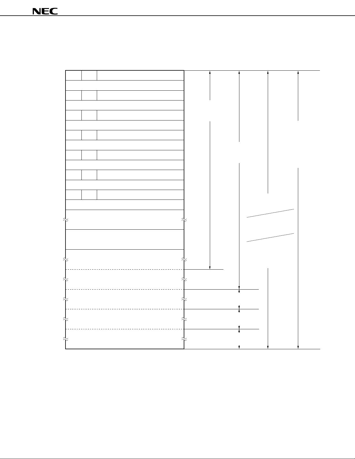
• Addresses 0000H and 0001H
Vector table wherein the program start address and the values set for the RBE and MBE at the time a RESET signal is
generated are written. Reset start is possible from any address.
• Addresses 0002H to 000DH
Vector table wherein the program start address and the values set for the RBE and MBE by each vectored interrupt are
written. Interrupt processing can start from any address.
• Addresses 0020H to 007FH
Note
Table area referenced by the GETI instruction
Note The GETI instruction realizes a 1-byte instruction on behalf of any 2-byte/3-byte instruction, or two 1-byte
instructions. It is used to decrease the number of program steps.
.
18
µ
PD75P3036
Figure 6-2 shows the addressing ranges for the program memory, branch instruction and the subroutine call instruction.
Figure 6-2. Program Memory Map
765 0
MBE
RBE
0000H
0002H
0004H
0006H
0008H
000AH
MBE
MBE
MBE
MBE
MBE
Internal reset start address (upper 6 bits)
Internal reset start address (lower 8 bits)
RBE
INTBT/INT4 start address (upper 6 bits)
INTBT/INT4 start address (lower 8 bits)
RBE
INT0 start address (upper 6 bits)
INT0 start address (lower 8 bits)
RBE
INT1 start address (upper 6 bits)
INT1 start address (lower 8 bits)
RBE
INTCSI start address (upper 6 bits)
INTCSI start address (lower 8 bits)
RBE
INTT0 start address (upper 6 bits)
CALLF
!faddr instruction
entry address
!caddr instruction
BRCB
branch address
Branch address
for the following
instructions
• BR BCXA
• BR BCDE
• BR !addr
• BRA !addr1
• CALLA !addr1
Note
Note
000CH
0020H
007FH
0080H
07FFH
0800H
0FFFH
1000H
1FFFH
2000H
2FFFH
3000H
3FFFH
MBE
INTT0 start address (lower 8 bits)
RBE
INTT1, INTT2 start address (upper 6 bits)
INTT1, INTT2 start address (lower 8 bits)
Reference table for GETI instruction
CALL !addr instruction
BR $addr instruction
relative branch address
BRCB
!caddr instruction
branch address
BRCB
!caddr instruction
branch address
BRCB
!caddr instruction
branch address
subroutine
entry address
Branch/call
address
by GETI
(–15 to –1,
+2 to +16)
*
Note Can be used only in the Mk II mode.
Remark For instructions other than those noted above, the BR PCDE and BR PCXA instructions can be used to branch
to addresses with changes in the PC’s lower 8 bits only.
19
µ
PD75P3036
6.3 Data Memory (RAM) ... 768 x 4 bits
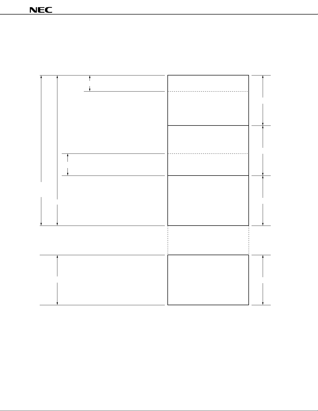
Figure 6-3 shows the data memory configuration.
Data memory consists of a data area and a peripheral hardware area. The data area consists of 768 x 4-bit static RAM.
Figure 6-3. Data Memory Map
Data area
static RAM
(768 x 4)
Display data memory
Stack area
Note
General-purpose register area
Data memory
000H
(32 x 4)
01FH
020H
256 x 4
(224 x 4)
0FFH
100H
256 x 4
(236 x 4)
1EBH
1ECH
(20 x 4)
1FFH
200H
256 x 4
Memory bank
0
1
2
2FFH
F80H
Peripheral hardware area
FFFH
Note Memory bank 0, 1, or 2 can be selected as the stack area.
Not incorporated
128 x 4
15
20
 Loading...