NEC UPD75P048GC-AB8, UPD75P048CW Datasheet

DATA SHEET
MOS INTEGRATED CIRCUIT
µ
PD75P048
4-BIT SINGLE-CHIP MICROCOMPUTER
DESCRIPTION
The µPD75P048 is a One-Time PROM version of the µPD75048. The µPD75P048 is suitable for small-scale
production or experimental production in system development.
Detailed functions are described in the following user’s manual. Read this manual when designing your
system.
µ
PD75048 User’s Manual: IEU-1278
FEATURES
• The
• 8064 × 8 bits of one-time programmable ROM
• 512 × 4 bits of RAM
• 1024 × 4 bits of EEPROM (Data memory area)
• Ports 0 to 3 and 6 to 8 with software-selectable pull-up resistors
• Port 9 with software-selectable pull-down resistors
• 12 N-channel open drain input/output ports (ports 4, 5, and 10)
• Low-voltage operation possible (VDD = 2.7 to 6.0 V)
µ
PD75048 compatible
• The µPD75P048 for evaluation/pre-production, while the µPD75048 for mass-production
ORDERING INFORMATION
Part number Package Quality grade
µ
PD75P048CW 64-pin plastic shrink DIP (750 mil) Standard
µ
PD75P048GC-AB8 64-pin plastic QFP ( 14 mm) Standard
Caution Pull-up/pull-down resistor mask options are not available.
Please refer to "Quality grade on NEC Semiconductor Devices" (Document number IEI-1209) published by
NEC Corporation to know the specification of quality grade on the devices and its recommended applications.
Document No. IC-3239
(O.D. No. IC-8720)
Date Published August 1994 P
Printed in Japan
The information in this document is subject to change without notice.
The mark ★ shows major revised points.
©
1994
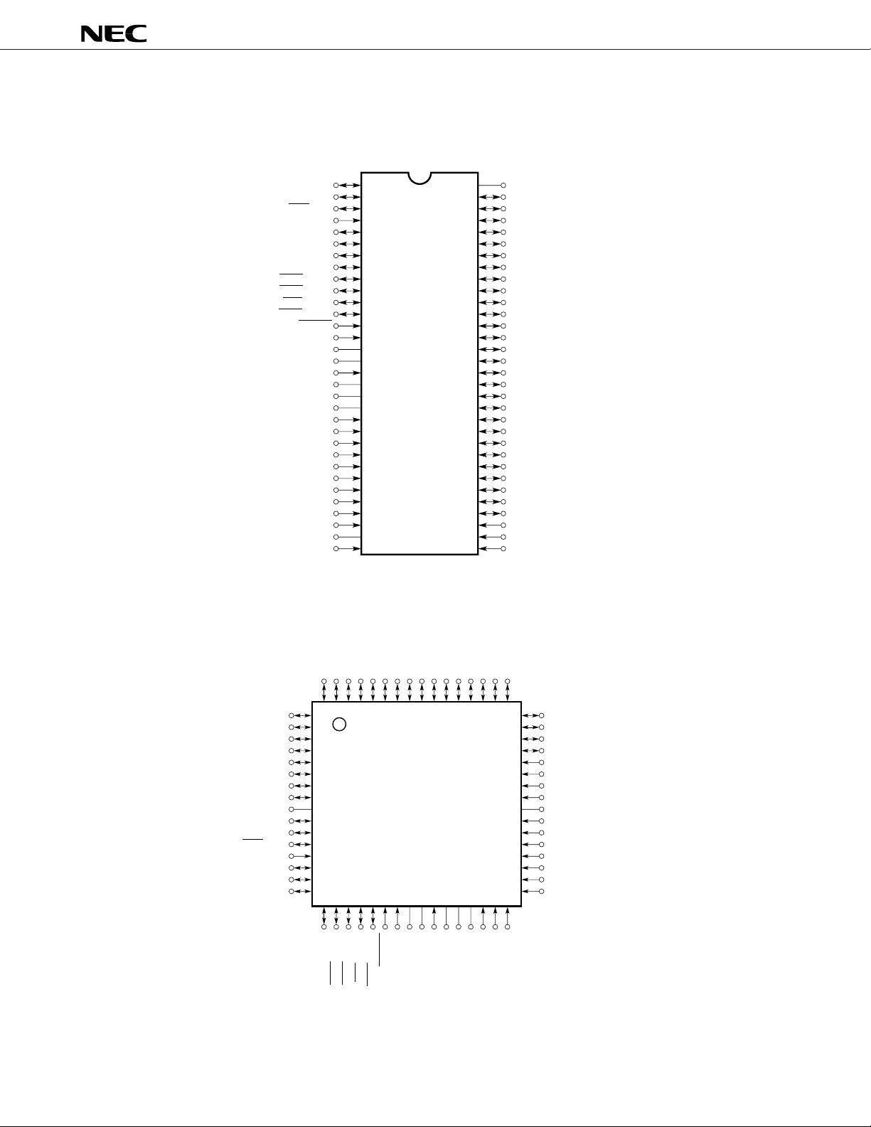
PIN CONFIGURATION (Top View)
• 64-pin plastic shrink DIP
µ
PD75P048
• 64-pin plastic QFP
SB1/SI/P03
SB0/SO/P02
SCK/P01
INT4/P00
BUZ/P23
PCL/P22
PPO/P21
PTO0/P20
MAT/P103
MAZ/P102
MAI/P101
MAR/P100
RESET
X1
X2
V
XT1
XT2
V
AVDD
AVREF+
AVREF–
AN7
AN6
AN5
AN4
AN3/P113
AN2/P112
AN1/P111
AN0/P110
AV
TI0/P13
1
2
3
4
5
6
7
8
9
10
11
12
13
14
µ
PD75P048CW
15
16
PP
17
18
19
DD
20
21
22
23
24
25
26
27
28
29
30
31
SS
32
64
63
62
61
60
59
58
57
56
55
54
53
52
51
50
49
48
47
46
45
44
43
42
41
40
39
38
37
36
35
34
33
V
SS
P30/MD0
P31/MD1
P32/MD2
P33/MD3
P40
P41
P42
P43
P50
P51
P52
P53
P60/KR0
P61/KR1
P62/KR2
P63/KR3
P70/KR4
P71/KR5
P72/KR6
P73/KR7
P80
P81
P82
P83
P90
P91
P92
P93
P10/INT0
P11/INT1
P12/INT2
P43
P42
P41
P40
MD3/P33
MD2/P32
MD1/P31
MD0/P30
V
SB1/SI/P03
SB0/SO/P02
SCK/P01
INT4/P00
BUZ/P23
PCL/P22
PPO/P21
P50
P51
P52
P53
P60/KR0
P61/KR1
P62/KR2
P63/KR3
64 63 62 61 60 59 58 57 56 55 54 53 52 51 50 49
1
2
3
4
5
6
7
8
9
SS
10
11
12
13
14
15
16
17 18 19 20 21 22 23 24 25 26 27 28 29 30 31 32
µ
PD75P048GC-AB8
X1
X2
RESET
MAI/P101
PTO0/P20
MAT/P103
MAZ/P102
MAR/P100
P70/KR4
P71/KR5
P72/KR6
VPP
XT1
XT2
P73/KR7
P80
P81
VDD
AVDD
AVREF+
P82
AVREF–
P83
48
47
46
45
44
43
42
41
40
39
38
37
36
35
34
33
AN7
P90
P91
P92
P93
P10/INT0
P11/INT1
P12/INT2
TI0/P13
AV
SS
AN0/P110
AN1/P111
AN2/P112
AN3/P113
AN4
AN5
AN6
2

µ
PD75P048
PIN IDENTIFICATION
P00-03 : Port0
P10-13 : Port1
P20-23 : Port2
P30-33 : Port3
P40-43 : Port4
P50-53 : Port5
P60-63 : Port6
P70-73 : Port7
P80-83 : Port8
P90-93 : Port9
P100-103 : Port10
P110-113 : Port11
KR0-7 : Key Return
SCK : Serial Clock
SI : Serial Input
SO : Serial Output
SB0, 1 : Serial Bus 0, 1
RESET : Reset Input
TI0 : Timer Input 0
PTO0 : Programmable Timer Output 0
BUZ : Buzzer Clock
PCL : Programmable Clock
INT0,1,4 : External Vectored Interrupt 0, 1, 4
INT2 : External Test Input 2
X1, 2 : Main System Clock Oscillation 1, 2
XT1, 2 : Subsystem Clock Oscillation 1, 2
MAR : Reference Integration Control
MAI : Integration Control
MAZ : Autozero Control
MAT : External Comparate Timing Input
PPO : Programmable Pulse Output ... MFT timer mode
AN0-7 : Analog Input 0-7
AVREF+ : Analog Reference (+)
REF- : Analog Reference (-)
AV
AVDD : Analog VDD
AVSS : Analog VSS
VDD : Positive Power Supply
VSS : Ground
VPP : Programming Power Supply
MD0-MD3 : Mode Selection
MFT
A/D
mode
★
Remarks MFT: Multi-function timer
3
4
TI0/P13
PTO0/P20
BASIC
INTERVAL
TIMER
INTBT
TIMER/
COUNTER
#0
INTT0
PROGRAM
COUNTER
SP
CY
ALU
BIT SEQ.
BUFFER
PORT 0
PORT 1 P10 - P13
P00 - P03
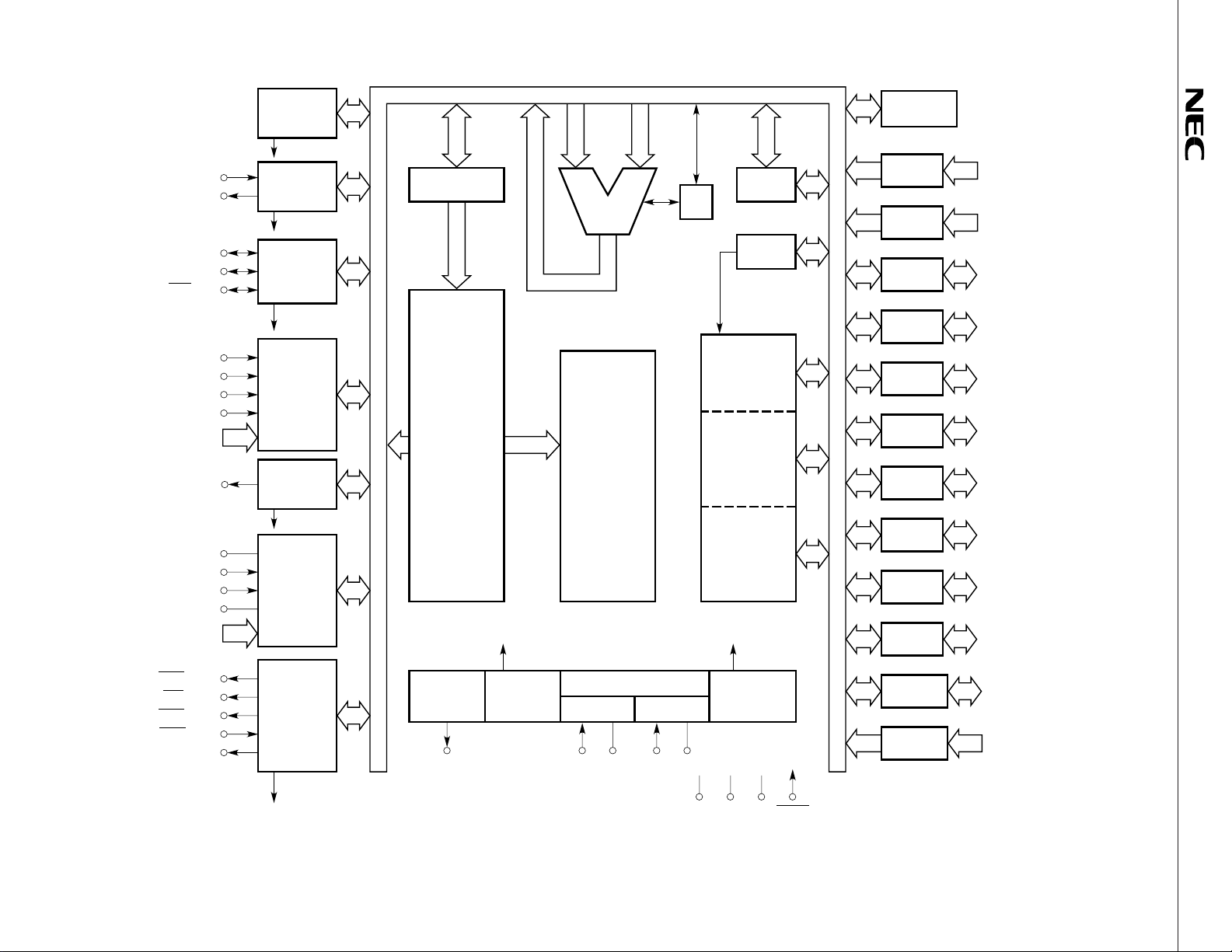
BLOCK DIAGRAM
SI/SB1/P03
SO/SB0/P02
SCK/P01
INT0/P10
INT1/P11
INT2/P12
INT4/P00
KR0 - KR3/P60 - P63
KR4 - KR7/P70 - P73
BUZ/P23
AVDD
AVREF+
AVREF–
AVSS
AN0 - AN3/P110 - P113
AN4 - AN7
MAR/P100
MAI/P101
MAZ/P102
MAT/P103
PPO/P21
SERIAL
INTERFACE
INTCSI
INTERRUPT
CONTROL
WATCH
TIMER
INTW
A/D
CONVERTER
MULTIFUNCTION
TIMER
PROM
PROGRAM
MEMORY
8064 × 8 BITS
CLOCK
OUTPUT
CONTROL
PCL/P22
N
fx/2
CLOCK
DIVIDER
DECODE
AND
CONTROL
CLOCK GENERATOR
SUB
XT1 XT2
MAIN
X1 X2
BANK
DATA
MEMORY
GENERAL REG.
RAM
512 × 4 BITS
EEPROM
1024 × 4 BITS
CPU CLOCK
Φ
STAND BY
CONTROL
PORT 2 P20 - P23
PORT 3 P30/MD0 - P33/MD3
PORT 4 P40 - P43
PORT 5 P50 - P53
PORT 6 P60 - P63
PORT 7 P70 - P73
PORT 8 P80 - P83
PORT 9 P90 - P93
PORT 10 P100 - P103
PORT 11 P110 - P113
µ
PD75P048
INTMFT
VSSVDDVPP
RESET

µ
PD75P048
CONTENTS
1. PIN FUNCTIONS ························································································································· 6
1.1 PORT PINS ·········································································································································· 6
1.2 NON-PORT PINS ································································································································· 8
1.3 PIN INPUT/OUTPUT CIRCUITS ········································································································ 10
2. DIFFERENCES BETWEEN THE µPD75P048 AND THE µPD75048 ······································· 13
3. PROM (PROGRAM MEMORY) WRITE AND VERIFY····························································· 14
3.1 PROM WRITE AND VERIFY OPERATION MODE ·········································································· 14
3.2 PROM WRITE PROCEDURE ·············································································································· 15
3.3 PROM READ PROCEDURE ················································································································ 16
4. SCREENING OF ONE-TIME PROM MODEL··········································································· 17
5. ELECTRICAL SPECIFICATIONS ·································································································· 18
6. PERFORMANCE CURVE (REFERENCE VALUE) ····································································· 32
7. PACKAGE DRAWINGS··············································································································· 34
8. RECOMMENDED SOLDERING CONDITIONS ········································································· 36
APPENDIX A. DEVELOPMENT TOOLS ·························································································· 37
APPENDIX B. RELATED DOCUMENTS ·························································································· 38
★
★
★
★
★
★
5
1. PIN FUNCTIONS
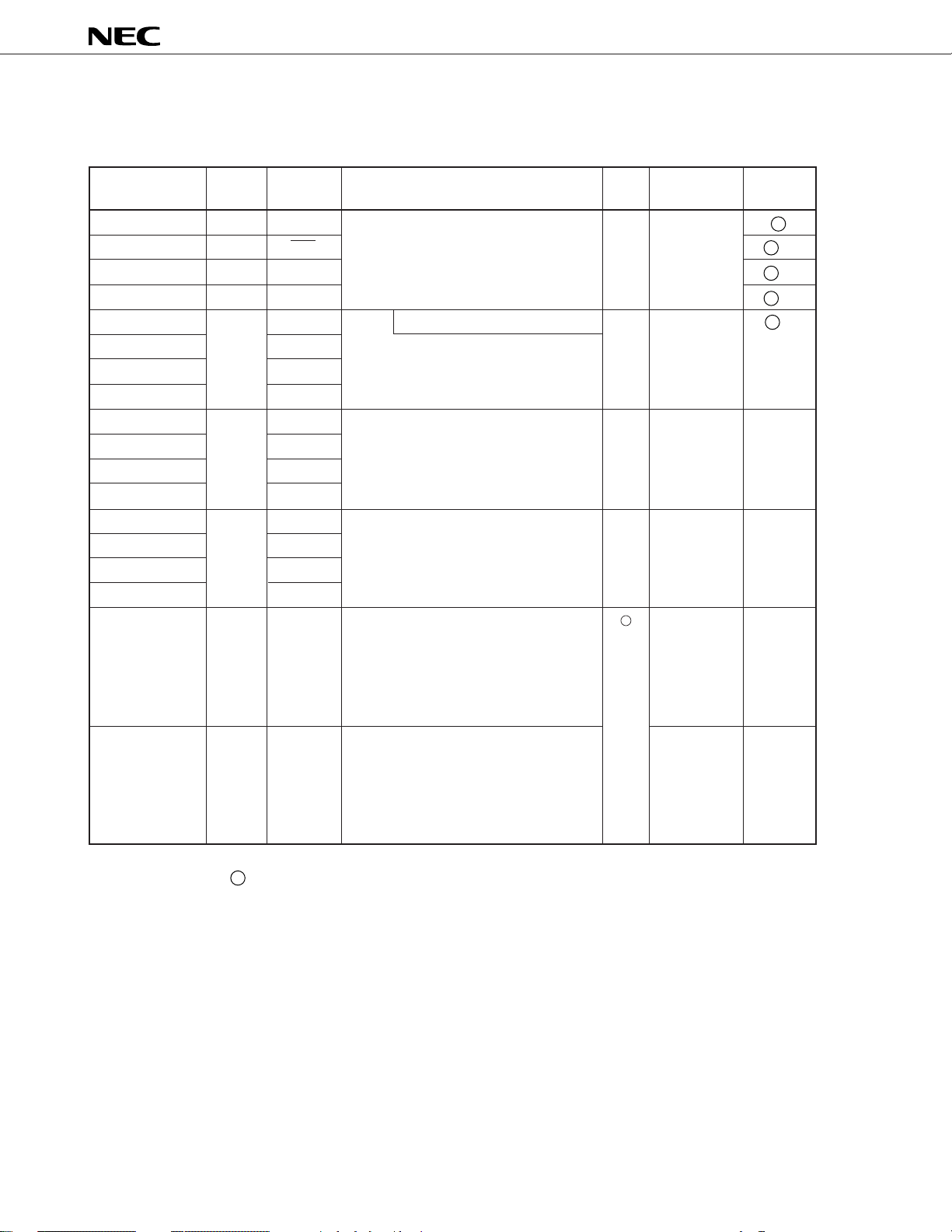
1.1 PORT PINS (1/2)
µ
PD75P048
Pin Name
P00
P01
P02
P03
P10
P11
P12
P13
P20
P21
P22
P23
Note 2
P30
Note 2
P31
Note 2
P32
Note 2
P33
P40 - P43
Note 2
Input/
Output
Input
I/O
I/O
I/O
Input
I/O
I/O
I/O
Shared
Pin
INT4
SCK
SO/SB0
SI/SB1
INT0
INT1
INT2
TI0
PTO0
PPO
PCL
BUZ
MD0
MD1
MD2
MD3
–
Function
4-bit input port (PORT0).
For P01 to P03, pull-up resistors can be
provided by software in units of 3 bits.
With noise elimination function
4-bit input port (PORT1).
Pull-up resistors can be provided by
software in units of 4 bits.
4-bit I/O port (PORT2).
Pull-up resistors can be provided by
software in units of 4 bits.
Programmable 4-bit I/O port (PORT3).
I/O can be specified bit by bit.
Pull-up resistors can be provided by
software in units of 4 bits.
N-ch open-drain 4-bit I/O port (PORT4).
Can withstand 10 V.
Data input/output pins for the PROM
write and verity (Four low-order bits).
8-Bit
I/O
×
×
×
×
When Reset
Input
Input
Input
Input
High
impedance
I/O Circuit
Note 1
Type
B
-A
F
-B
F
-C
M
-C
B
E-B
E-B
M-A
P50 - P53
Note 2
I/O
–
N-ch open-drain 4-bit I/O port (PORT5).
Can withstand 10 V.
Data input/output pins for the PROM
write and verify (Four high-order bits).
Note 1. The circle ( ) indicates the Schmitt trigger input.
2. Can directly drive LEDs.
High
impedance
M-A
6

1.1 PORT PINS (2/2)
µ
PD75P048
Pin Name
P60
P61
P62
P63
P70
P71
P72
P73
P80 - P83
P90 - P93
P100
P101
P102
P103
P110
P111
P112
P113
Input/
Output
I/O
I/O
I/O
I/O
I/O
Input
Shared
Pin
KR0
KR1
KR2
KR3
KR4
KR5
KR6
KR7
–
–
MAR
MAI
MAZ
MAT
AN0
AN1
AN2
AN3
Function
Programmable 4-bit I/O port (PORT 6).
Pull-up resistors can be provided by
software in units of 4 bits.
4-bit I/O port (PORT 7).
A pull-up resistor can be provided by
software in units of 4 bits
4-bit I/O port (PORT 8).
A pull-up resistor can be provided by
software in units of 4 bits.
4-bit I/O port (PORT 9).
A pull-up resistor can be provided by
software in units of 4 bits.
N-ch open drain 4-bit I/O port (PORT 10).
Can withstand 10 V in open-drain
mode.
4-bit input port (PORT 11).
8-Bit
I/O
×
×
When Reset
Input
Input
Input
Input
High
impedance
Input
I/O Circuit
Note
Type
-A
F
-A
F
E-B
E-D
M-A
Y
★
Note The circle ( ) indicates the Schmitt trigger input.
7
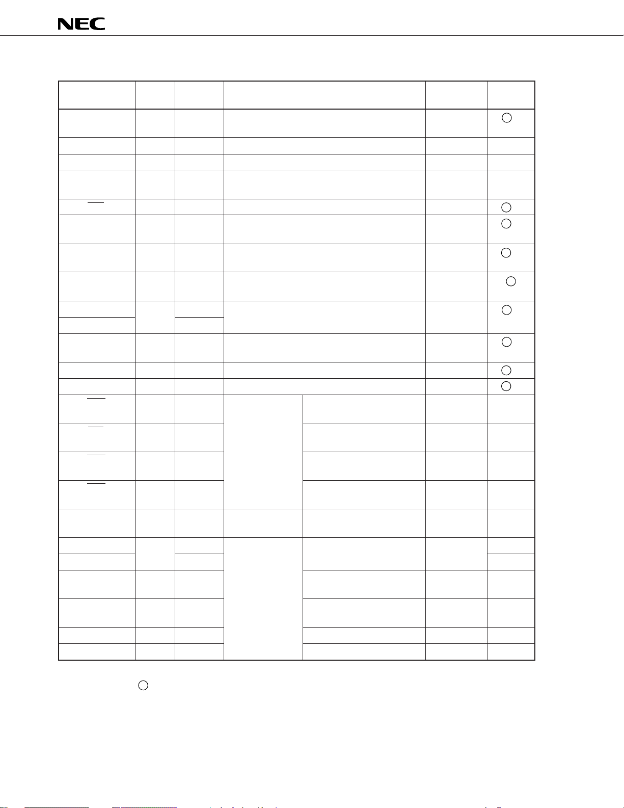
1.2 NON-PORT PINS (1/2)
µ
PD75P048
Pin Name
TI0
PTO0
PCL
BUZ
SCK
SO/SB0
SI/SB1
INT4
INT0
INT1
INT2
KR0 - KR3
KR4 - KR7
MAR
MAI
MAZ
MAT
PPO
AN0 - AN3
AN4 - AN7
AVREF+
AVREF–
AVDD
AVSS
Input/
Output
Input
I/O
I/O
I/O
I/O
I/O
I/O
Input
Input
Input
I/O
I/O
I/O
I/O
I/O
I/O
I/O
Input
Input
Input
–
–
Shared
Pin
P13
P20
P22
P23
P01
P02
P03
P00
P10
P11
P12
P60 - P63
P70 - P73
P100
P101
P102
P103
P21
P110 - P113
–
–
–
–
–
Function
Input for receiving external event pulse signal
for timer/event counter
Timer/event counter output
Clock output
Output for arbitrary frequency output (for
buzzer output or system clock trimming)
Serial clock I/O
Serial data output
Serial bus I/O
Serial data input
Serial bus I/O
Edge detection vectored interrupt input (either
rising edge or falling edge detection)
Edge detection vectored interrupt input
(detection edge selectable)
Edge detection testable input (rising edge
detection)
Parallel falling edge detection testable input
Parallel falling edge detection testable input
In MFT integrating A/D
converter mode
In MFT timer
mode
For A/D
converter only
Reverse integration signal
output
Integration signal output
Auto-zero signal output
Comparator input
Timer pulse output
8-bit analog input
Reference voltage input
(AVDD side)
Reference voltage input
(AVSS side)
Positive power supply
GND potential
When Reset
Input
Input
Input
Input
Input
Input
Input
Input
Input
Input
Input
Input
High
impedance
High
impedance
High
impedance
High
impedance
Input
–
–
–
–
–
I/O Circuit
Note
Type
-C
B
E-B
E-B
E-B
-A
F
-B
F
-C
M
B
-C
B
-C
B
-A
F
F
-A
M-A
M-A
M-A
M-A
E-B
Y-A
Y-A
Z-A
Z-A
–
–
Note The circle ( ) indicates the Schmitt trigger input.
Remark MFT: Multi-Function Timer
8

1.2 NON-PORT PINS (2/2)
µ
PD75P048
Pin Name
X1, X2
XT1, XT2
RESET
MD0 - MD3
Note 2
VPP
VDD
VSS
Input/
Output
Input
Input
Input
I/O
–
–
–
Shared
Pin
–
–
–
P30 - P33
–
–
–
Function
Crystal/ceramic resonator connection for main
system clock generation. When external clock
signal is used, it is applied to X1, and its
reverse phase signal is applied to X2.
Crystal connection for subsystem clock
generation. When external clock signal is
used, it is applied to XT1, and its reverse
phase signal is applied to XT2. XT1 can be
used as a 1-bit input (test).
System reset input
Operation mode selection pins during the
PROM write/verify cycles.
Normally connected to VDD directly; +12.5 V is
applied as the programming voltage during the
PROM write/verify cycles.
Positive power supply
GND potential
When Reset
–
–
–
Input
–
–
–
Note 1. The circle ( ) indicates the Schmitt trigger input.
2. The VPP should be connected to VDD directly in normal operation mode. If VPP and VDD pins are not
µ
connected, the
PD75P048 does not operate correctly.
I/O Circuit
Note 1
Type
–
–
B
E-B
–
–
–
9
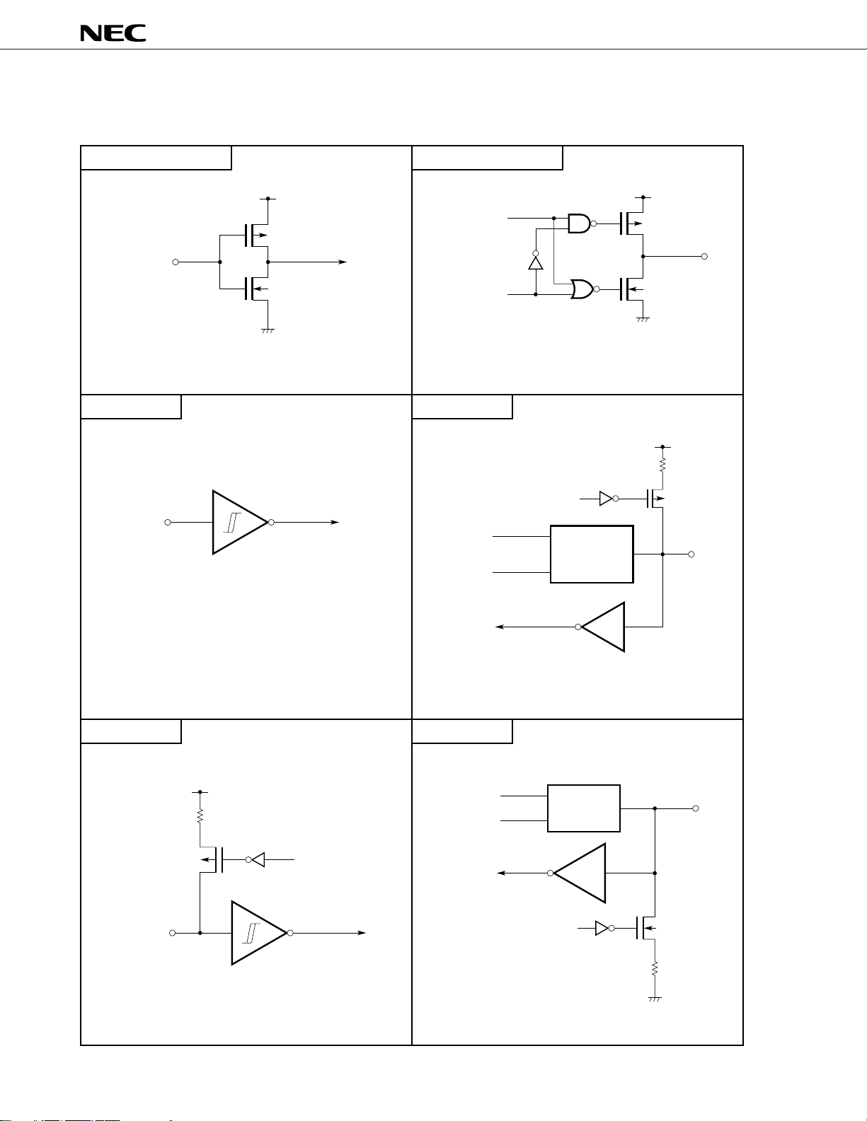
1.3 PIN INPUT/OUTPUT CIRCUITS
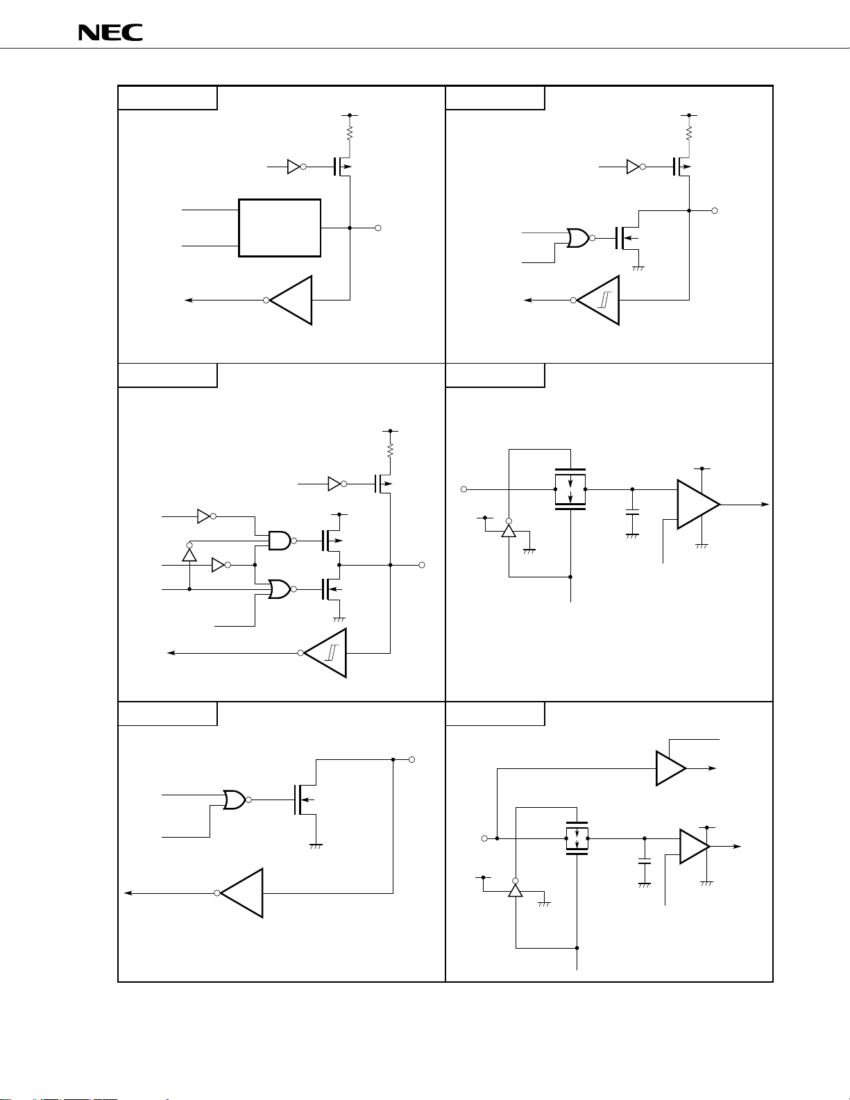
The input/output circuit of each µPD75P048 pin is shown below in a simplified manner.
Type A (For Type E-B)
Type D (For Type E-B, F-A)
µ
PD75P048
(1/3)
Type B
VDD
Data
P-ch
IN
N-ch
CMOS input buffer
Type E-B
IN
Output
disable
Push-pull output which can be set to high-impedance output
(off for both P-ch and N-ch)
P.U.R.
enable
Data
Output
disable
Type D
VDD
P-ch
OUT
N-ch
VDD
P.U.R.
P-ch
IN/OUT
Schmitt trigger input with hysteresis
Type B-C Type E-D
VDD
P.U.R.
P-ch
IN
P.U.R.: Pull-Up Resistor P.D.R.: Pull-Down Resistor
P.U.R.
enable
Data
Output
disable
Type A
P.U.R.: Pull-Up Resistor
Type D
Type A
P.D.R.
enable
IN/OUT
N-ch
P.D.R.
10
Type F-A Type M-C
VDD
µ
PD75P048
VDD
(2/3)
Output
disable
Type F-B
Output
disable
(P)
Data
Output
disable
Data
Output
disable
(N)
P.U.R.
enable
Type D
Type B
P.U.R.: Pull-Up Resistor
P.U.R.
enable
VDD
P-ch
N-ch
P.U.R.
P-ch
IN/OUT
VDD
P.U.R.
P-ch
IN/OUT
Output
disable
Type Y
IN
AVDD
Data
P.U.R.
enable
P.U.R.: Pull-Up Resistor
P-ch
N-ch
AVSS
Sampling C
Input
enable
P.U.R.
P-ch
IN/OUT
N-ch
AVDD
+
–
AVSS
Reference voltage
(from voltage tap of
series resistor string)
P.U.R.: Pull-Up Resistor
Type M-A Type Y-A
IN/OUT
Data
Output
disable
Middle-voltage input buffer
(Can withstand + 10 V)
P.U.R.: Pull-Up Resistor
N-ch
(Can with stand + 10 V)
AVDD
IN
P-ch
N-ch
AVSS
Input buffer
+
Sampling C
Reference voltage
(from voltage tap of
series resistor string)
–
IN instruction
AVDD
AVSS
11
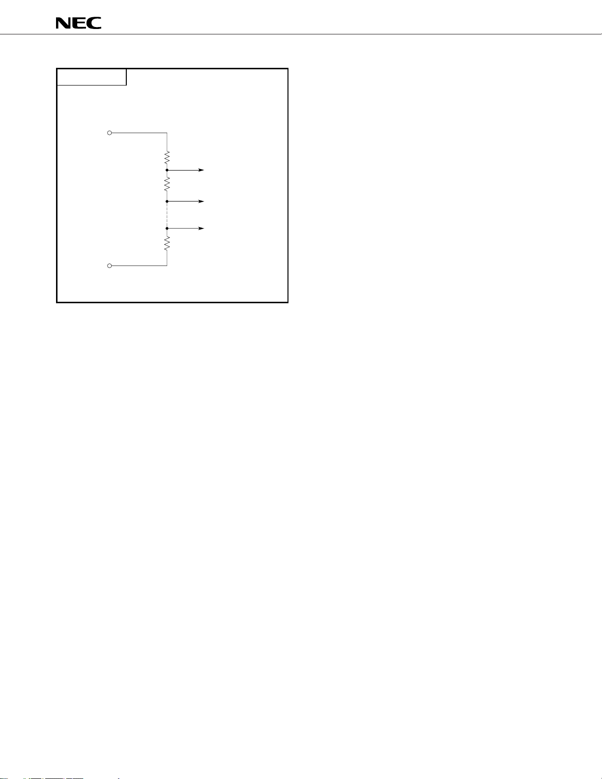
Type Z-A
AVREF+
AVREF–
Reference voltage
(3/3)
µ
PD75P048
12
 Loading...