NEC UPD72042AGT, UPD72042BGT Datasheet
DATA SHEET
MOS INTEGRATED CIRCUIT
µ
PD72042A, 72042B
LSI DEVICES FOR Inter Equipment BusTM (IEBusTM)
PROTOCOL CONTROL
The µPD72042A and µPD72042B are microcomputer peripheral LSI devices for IEBus protocol control.
µ
PD72042A and µPD72042B perform all the processing required for layers 1 and 2 of the IEBus. The devices
The
incorporate large transmission and reception buffers, allowing the microcomputer to perform IEBus operations without
interruption. They also contain an IEBus driver and receiver, allowing them to directly connected to the bus directly.
FEATURES
Control of layers 1 and 2 of the IEBus protocol
••
• Support of a multi-master scheme
• Broadcast function
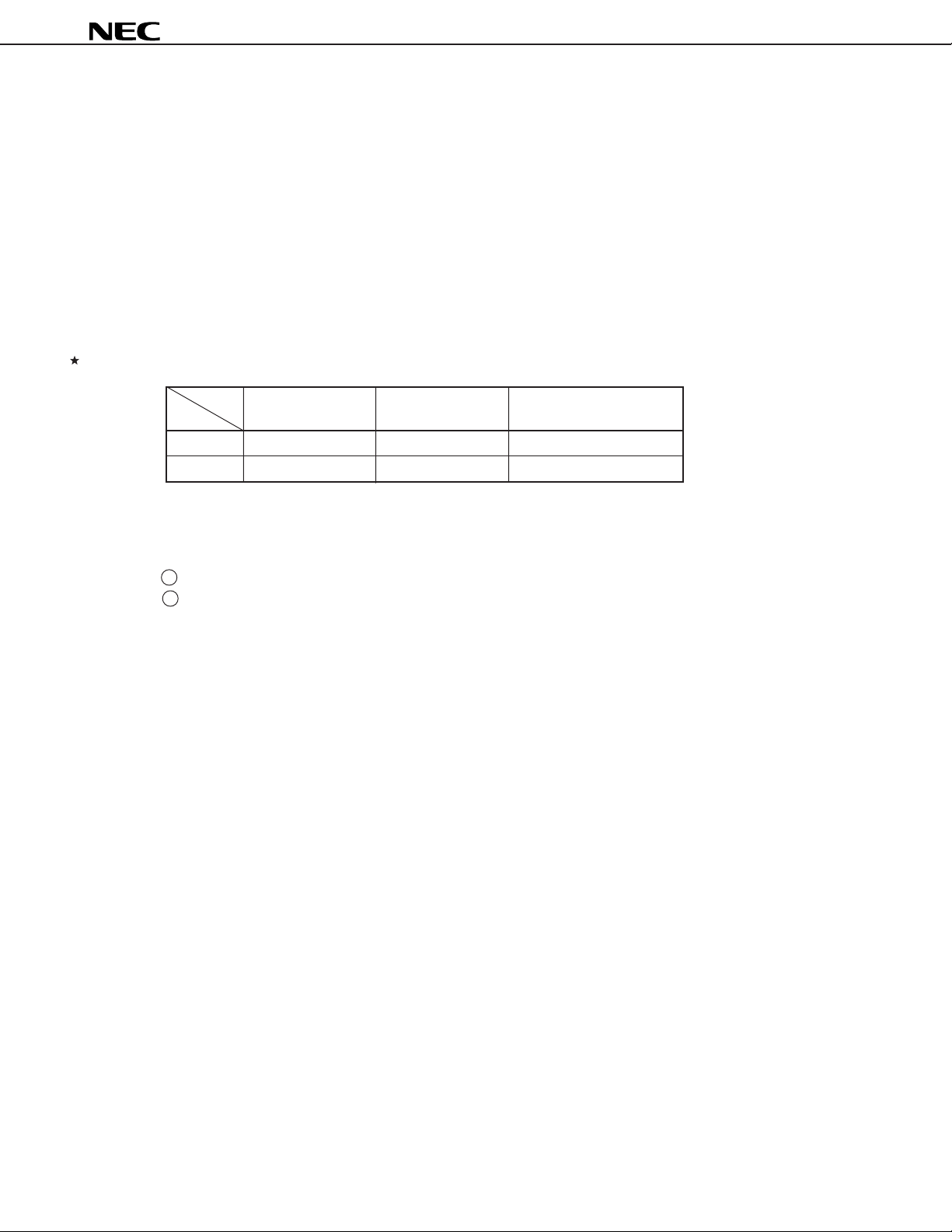
• Two communication modes having different
transmission speeds can be selected.
When operating When operating
at 6 MHz at 6.29 MHz
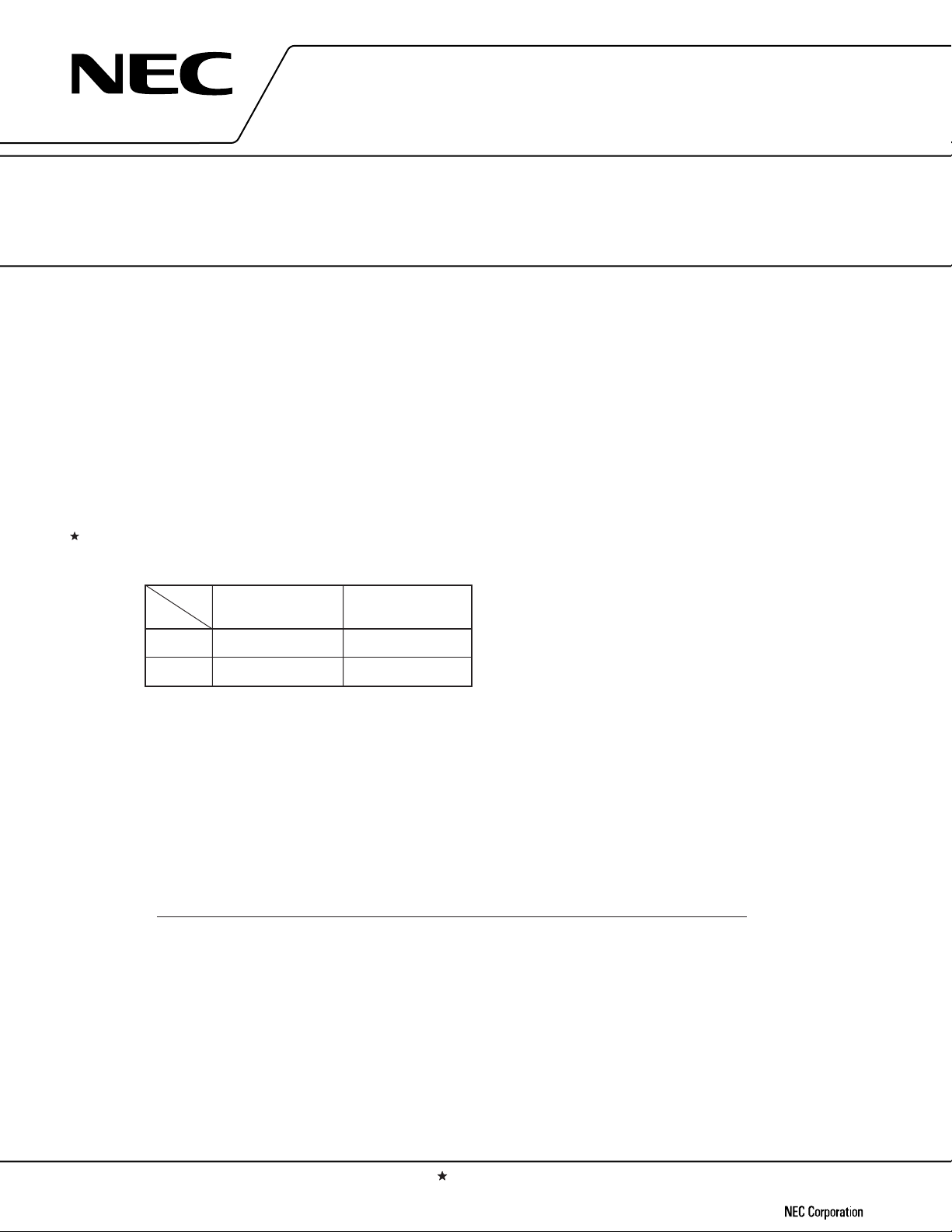
Mode 0 Approx. 3.9 Kbps Approx. 4.1 Kbps
Mode 1 Approx. 17 Kbps Approx. 18 Kbps
Built-in IEBus driver and receiver
●●
●● Transmission and reception buffers
Transmission buffer : 33 bytes, FIFO
Reception buffer : 40 bytes, FIFO (capable of
holding more than one frame
of reception data.)
Microcomputer interface
••
Three-/two-wire serial I/O
µ
• Transfer starting with MSB :
• Transfer starting with LSB :µPD72042B
Program crashes can be detected by means of a
••
watchdog timer.
Low power consumption (standby mode):
••
µ
A (max)
50
Oscillator frequency (fX): 6 MHz, 6.29 MHz
••
• frequency accuracy: ±1.5%
Operating voltage: 5 V ±10%
••
PD72042A
ORDERING INFORMATION
Part number Package Starting with MSB/LSB
µ
PD72042AGT 16-pin plastic SOP (375 mil) MSB
µ
PD72042BGT 16-pin plastic SOP (375 mil) LSB
Document No. S13990EJ2V0DS00 (2nd edition)
(Previous No. ID-3649)
Date Published January 1999 N CP(N)
Printed in Japan
The information in this document is subject to change without notice.
The mark shows major revised points.
©
1995
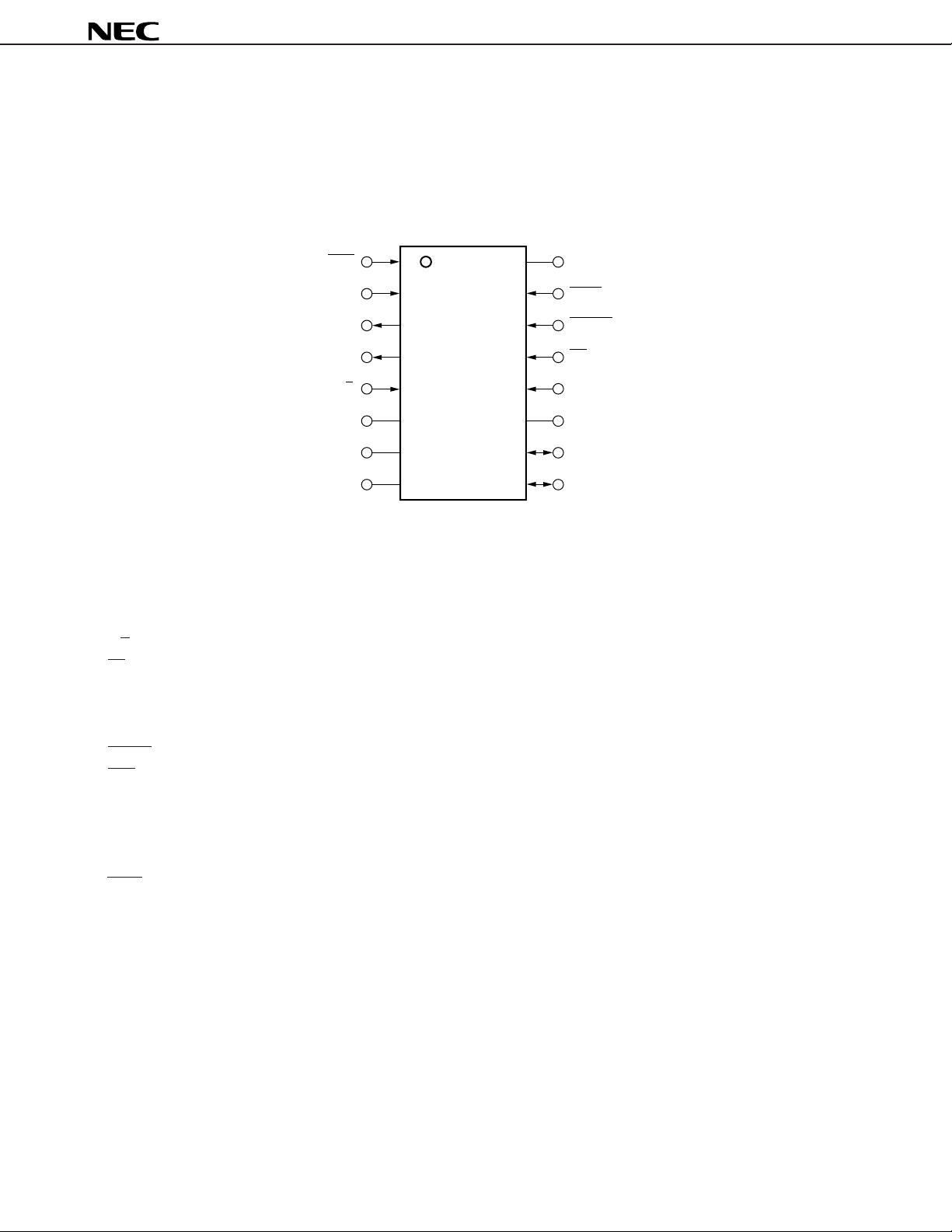
PIN CONFIGURATION (TOP VIEW)
• 16-pin plastic SOP (375 mil)
µ
PD72042AGT
µ
PD72042BGT
µ
PD72042A, 72042B
SI(SIO)
SO(NC)
SCK
Note
Note
IRQ
C/D
XO
GND
1
2
3
4
5
XI
6
7
8
16
15
14
13
12
11
10
9
V
DD
TEST
RESET
CS
SEL
DD
AV
BUS+
BUS−
Note Parentheses indicate the state corresponding to two-wire serial I/O mode.
AVDD : Main power supply for IEBus (connected to the VDD pin)
BUS–, BUS+ : IEBus I/O
C/D : Command/data switch input
CS : Chip select input
GND : Ground
IRQ : Interrupt request output
NC : No connection
RESET : Reset input
SCK : Serial clock input
SEL : Serial mode selection
SI : Serial data input
SIO : Serial data I/O
SO : Serial data output
TEST : Test input (connected to the V
DD pin)
VDD : Main power supply
XI, XO : System clock
2
DATA SHEET S13990EJ2V0DS00
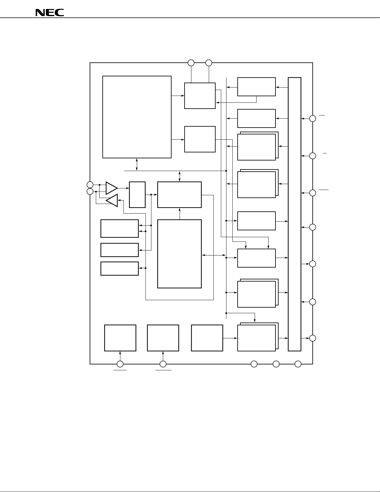
BLOCK DIAGRAM
XI XO
µ
PD72042A, 72042B
BUS +
BUS –
Data link controller
Internal bus
Receiver
Driver
Contention
detection
section
Parity generation
section
Parity detection
section
Filter
Oscillation
control
section
Program
detection
section
P/S conversion
section
Synchronization
control section
crash
CTR
CMR
WDB
(5 bytes)
TBF
(33 bytes)
STR
FLG
CS
C/D
SCK
SI
(SIO)
Serial I/O control section
SO
(NC)
RDB
(7 bytes)
Frame data
control
section
RBF
(40 bytes)
DD
V
DD
Test circuit
TEST
Timing
generation
section
RESET AV
Remark The pin names in parentheses are used when two-wire serial I/O is selected.
SEL
IRQ
GND
DATA SHEET S13990EJ2V0DS00
3

µ
PD72042A, 72042B
CONTENTS
1. PIN FUNCTIONS ............................................................................................................................. 6
1.1 PIN FUNCTIONS..................................................................................................................................... 6
2. IEBus OPERATION......................................................................................................................... 8
2.1 OVERVIEW.............................................................................................................................................. 8
2.2 IEBus COMMUNICATION PROTOCOL ................................................................................................ 9
2.2.1 Bus Mastership Determination (Arbitration) ............................................................................... 10
2.2.2 Communication Mode ................................................................................................................. 1 0
2.2.3 Communication Address ............................................................................................................. 11
2.2.4 Broadcast..................................................................................................................................... 11
2.3 TRANSMISSION PROTOCOL ............................................................................................................... 11
2.4 TRANSMISSION DATA (CONTENTS OF THE DATA FIELD) ............................................................. 17
2.5 BIT FORMAT........................................................................................................................................... 21
3. MICROCOMPUTER INTERFACE .................................................................................................. 22
3.1 TRANSFER METHOD ............................................................................................................................ 22
3.2 DATA TRANSFER FORMAT .................................................................................................................. 23
3.2.1 Three-Wire Data Transfer (SEL = 1) .......................................................................................... 2 3
3.2.2 Two-Wire Data Transfer (SEL = 0) ............................................................................................. 2 6
3.3 CONNECTION TO A MICROCOMPUTER ............................................................................................. 29
3.4 STANDBY MODE SETTING AND CANCELLATION............................................................................ 30
3.5 RESET MODE SETTING AND CANCELLATION................................................................................. 30
4. REGISTERS .................................................................................................................................... 31
5. EXAMPLE TIMINGS FOR COMMUNICATION.............................................................................. 61
6. EXAMPLE MICROCOMPUTER PROCESSING FLOW ................................................................ 69
6.1 COMMUNICATION FLAGS .................................................................................................................... 70
6.2 MAIN ROUTINE ...................................................................................................................................... 71
6.3 INTERRUPT ROUTINE........................................................................................................................... 72
6.4 PROCESSING ROUTINES ..................................................................................................................... 74
µ
6.4.1
6.4.2 Communication Flag Initialization Routine................................................................................. 74
6.4.3 Command Processing Routine ................................................................................................... 7 5
6.4.4 Master Communication Processing Routine.............................................................................. 75
6.4.5 Slave Data Transmission Processing Routine........................................................................... 79
6.4.6 Transmission Processing Routine .............................................................................................. 8 2
6.4.7 Reception Processing Routine ................................................................................................... 83
PD72042A or µPD72042B Initial Setting Routine.................................................................... 74
7. ELECTRICAL CHARACTERISTICS .............................................................................................. 84
8. PACKAGE DRAWING..................................................................................................................... 88
4
DATA SHEET S13990EJ2V0DS00

µ
PD72042A, 72042B
9. RECOMMENDED SOLDERING CONDITIONS ............................................................................. 89
APPENDIX A MAIN DIFFERENCES BETWEEN µPD72042A, µPD72042B, AND µPD6708 ......... 90
APPENDIX B IEBus PROTOCOL ANALYZER .................................................................................. 90
DATA SHEET S13990EJ2V0DS00
5

1. PIN FUNCTIONS
1.1 PIN FUNCTIONS
µ
PD72042A, 72042B
Pin No.
1
2
3
4
5
6
7
8
9
10
11
12
13
Note
Pin
SCK
SI (SIO)
SO (NC)
IRQ
C/D
XI
XO
GND
BUS–
BUS+
AVDD
SEL
CS
Note
I/O
Input
Input (I/O)
Output
(none)
Output
Input
–
–
I/O
–
Input
Input
Function
Serial clock input pin for CPU interface
Serial data pin for CPU interface. (This pin
functions as an input pin when 3-wire serial
I/O mode is selected, or as an I/O pin when
2-wire serial I/O mode is selected.)
Serial data output pin for CPU interface. (The
pin functions as an output when 3-wire serial I/O
mode is selected. When 2-wire serial I/O mode
is selected, the pin is left open.)
Output pin for making an interrupt request to the
CPU. When a return code or a program crash is
detected, a high-level signal is output on this pin
for at least 8 µs.
Input pin used to select control mode or data
read/write mode. When this pin is driven high,
internal register address setting and data read/
write are enabled. When the mode changes, the
serial clock counter is reset.
Pins for connecting a system clock resonator. A
6- or 6.29-MHz crystal or ceramic resonator
must be used. The accuracy of the frequency is
as follows;
Mode 0, 1: ±1.5%
Ground pin
I/O pins connected to the IEBus bus
Main power supply pin for the IEBus bus driver/
receiver. When used, this pin must be tied to
VDD.
Input pin used to select either 3- or 2-wire serial
I/O mode. A high-level signal on this pin selects
3-wire serial I/O mode. A low-level signal on this
pin selects 2-wire serial I/O mode.
Chip select pin. When this pin is driven low, the
serial interface is enabled. When this pin is
driven high, the SO pin becomes high-impedance, and the serial clock counter is reset.
I/O format
CMOS input
CMOS input
(CMOS I/O)
CMOS output
(none)
CMOS output
CMOS input
–
–
–
–
CMOS input
CMOS input
Note
When reset
[for both hardware
and software]
Input
Input
High-impedance
Low level
Input
When reset by
hardware (Oscillation stopped)
XI = GND
XO = High level
When reset by
software (Oscillation continued)
–
High-impedance
–
Input
Input
Note Parentheses indicate the state corresponding to two-wire serial I/O mode.
6
DATA SHEET S13990EJ2V0DS00
µ
PD72042A, 72042B
Pin No.
14
15
16
Pin
RESET
TEST
VDD
Input
Input
–
I/O
Function
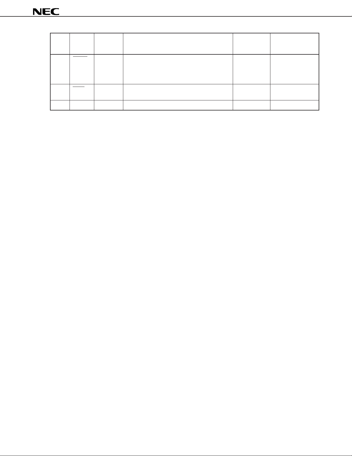
Serial reset signal input pin. A low input causes
a reset. Whenever the power is turned on, a
low-level signal must be applied to this pin.
During normal operation, a high level is applied.
IC test pin. When used, this pin must be tied to
the VDD pin directly.
Main power supply input pin
I/O format
CMOS input
CMOS input
–
When reset
[for both hardware
and software]
Input
–
–
DATA SHEET S13990EJ2V0DS00
7

µ
PD72042A, 72042B
2. IEBus OPERATION
2.1 OVERVIEW
µ
PD72042A and µPD72042B are CMOS LSI devices for the IEBus interface.
The
The IEBus is designed to enable the data transmission between devices in a small-scale digital data transmission
system.
µ
PD72042A and µPD72042B are connected to a microcomputer built into a device. A serial interface (SCK,
The
SO, and SI pins) is used for connection. The host controller (microcomputer) sets the commands and data needed
for data transmission via this serial interface.
µ
When data is transmitted, the host controller sets the data in the
Then, signals are output on the BUS pins (BUS+, BUS–). When data is received from the BUS pins, the host controller
can read it via the serial interface.
PD72042A or µPD72042B via the serial interface.
8
DATA SHEET S13990EJ2V0DS00
2.2 IEBus COMMUNICATION PROTOCOL
The IEBus is outlined below.
• Communication method: Half duplex asynchronous communication
• Multi-master method
All units connected to the IEBus can transmit data to every other connected unit.
• Broadcast function (one-unit-to-multiple-units communication)
Group broadcast : Broadcast to a specific group of units
General broadcast : Broadcast to all units
• Two modes, each offering different transmission speeds, can be selected.
µ
PD72042A, 72042B
fX = 6 MHz
Mode 0 Approx. 3.9 Kbps Approx. 4.1 Kbps 16
Mode 1 Approx. 17 Kbps Approx. 18 Kbps 32
fX = 6.29 MHz
Maximum number of bytes
transmitted (bytes/frame)
• Access control: Carrier Sense Multiple Access with Collision Detection (CSMA/CD)
Bus mastership priority is as follows:
1 Broadcast takes priority over ordinary communication (one-unit-to-one-unit communication).
2 Units having lower master addresses have a higher priority.
• Communication scale
Number of units : 50 max
Cable length : 150 m max (when twisted-pair cable is used <resistance 0.1 Ω/m or less>)
Load capacity : 8000 pF max <between BUS- and BUS+>, f
7100 pF max <between BUS- and BUS+>, f
X = 6 MHz
X = 6.29 MHz
Terminating resistance : 120 Ω
µ
Caution For the
PD72042A and µPD72042B, as a protective resistance, connect a 180-Ω resistor in series
with the BUS– and BUS+ pins.
DATA SHEET S13990EJ2V0DS00
9
µ
PD72042A, 72042B
2.2.1 Bus Mastership Determination (Arbitration)
Before devices connected to the IEBus can control other devices, they must first acquire the bus. This operation
is called arbitration.
When more than one unit starts transmission at the same time, arbitration determines which of those units is allowed
to use the bus.
When arbitration results in only one device being granted bus mastership, the following bus mastership priority
conditions are used:
Remark Those devices that are defeated in arbitration can automatically enter retransmission mode. (For the
µ
PD72042A and µPD72042B, the number of retransmissions can be set by specifying a value between
0 and 7 in the MCR register.)
(1) Priority by communication type
Broadcast (one-unit-to-multiple-units communication) takes priority over ordinary communication (one-unit-toone-unit communication).
(2) Priority by master address
If the communication type is the same, the smallest master address value has the highest priority.
Example Each master address consists of 12 bits. A unit having master address 000H has the highest priority,
while a unit having master address FFFH has the lowest priority.
2.2.2 Communication Mode
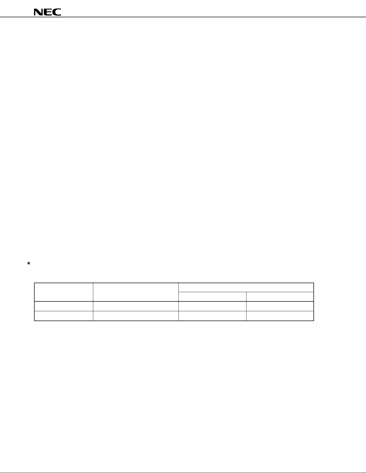
The IEBus supports two communication modes, each having a different transmission speed. Table 2-1 lists the
transmission speed for each communication mode and the maximum number of bytes transmitted within one
communication frame.
Table 2-1 Transmission Speed and Maximum Number of Transmission
Bytes in Each Communication Mode
Note 1
(Kbps)
fX = 6.29 MHz
Note 2
Communication mode
0 16 Approx. 3.9 Approx. 4.1
1 32 Approx. 17 Approx. 18
Maximum number of transmission
bytes (bytes/frame)
Effective transmission speed
fX = 6 MHz
Note 2
Notes 1. Effective transmission speed at which the maximum transfer rate is achieved
µ
2. Oscillator frequencies for the
PD72042A and µPD72042B
Cautions 1. Before devices connected to the IEBus can perform communication, an appropriate commu-
nication mode must be set. Note that if a master unit and an associated unit (slave unit) have
different communication modes, they will not be able to communicate properly.
2. Communication cannot be performed properly between a unit operating at an oscillator
frequency of 6 MHz and another operating at 6.29 MHz, even when set to the same communication
mode. Units must use the same oscillator frequency to be able to communicate.
10
DATA SHEET S13990EJ2V0DS00

µ
PD72042A, 72042B
2.2.3 Communication Address
With the IEBus, each device is assigned a unique 12-bit communication address. The communication address
consists of the following parts:
High-order 4 bits : Group number (number identifying the group to which a device belongs)
Low-order 8 bits : Unit number (number identifying a device in a group)
2.2.4 Broadcast
In ordinary communication, transmission and reception are performed between one master unit and one associated
slave unit. Broadcast can also be done between one master unit and more than one slave unit. In this case master
unit transmits data to an arbitrary number of slave units. In this case, the slave units do not return on acknowledge
signal to the master unit.
Whether the communication to be performed is broadcast or ordinary communication is determined by the setting
of the broadcast bit. (For details of the broadcast bit, see (1) 2 in Section 2.3.)
There are two types of broadcast.
(1) Group broadcast
Broadcast is performed to the devices in a particular group. These devices all have the same group number,
as indicated by the high-order 4 bits of each communication address.
(2) General broadcast
Broadcast is performed to all devices, regardless of their group numbers.
These two types of broadcast are distinguished by the slave address. (For details of the slave address, see (3)
in Section 2.3.)
2.3 TRANSMISSION PROTOCOL
Fig. 2-1 shows the IEBus transmission signal format.
Communication data is transmitted as a sequence of signals called a communication frame. The transmission
speed and the maximum amount of data that can be transmitted in one communication frame depend on the
communication mode.
DATA SHEET S13990EJ2V0DS00
11
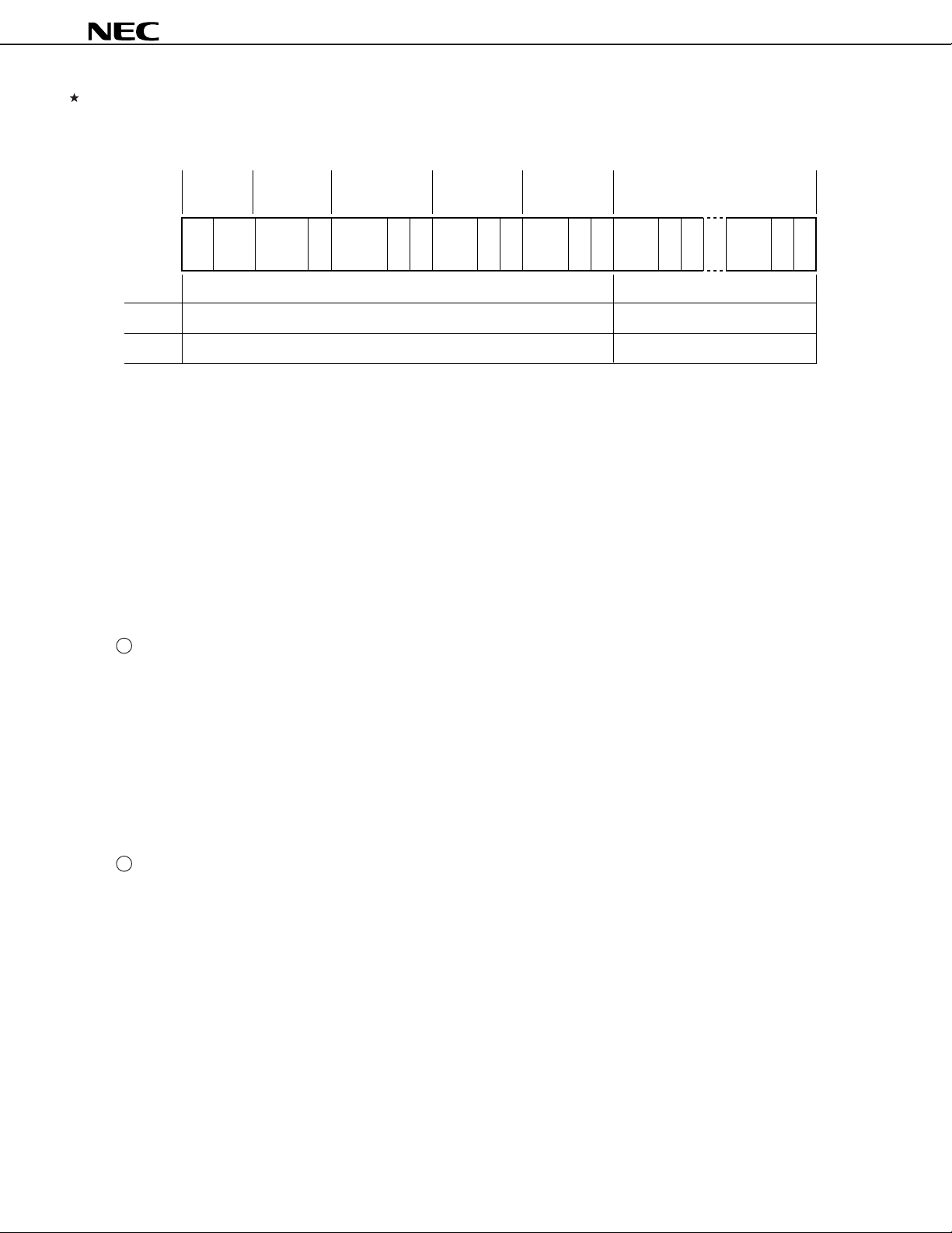
Fig. 2-1 Transmission Signal Format
µ
PD72042A, 72042B
(When f
X
= 6 MHz)
Field name
Number of bits
Transmission
time
Mode 0
Mode 1
Header
11
Broad-
Start
cast
bit
bit
Master
address field
12 1
Master
address
Slave
address field
12 1 1
P Slave
address
Approx. 7330
Approx. 2090
Control field
411
P A Control
bits
s
µ
s
µ
PA
Data-length
field
811
Data-
length
P A Data
bits
P : Parity bit (1 bit)
A : Acknowledge bit (1 bit)
When A = 0: ACK
When A = 1: NAK
N : Number of data bytes
Remark For broadcast, the value of the acknowledge bit is ignored.
(1) Header
The header consists of a start bit and a broadcast bit. These are explained below.
Data field
811 811
P A Data
bits
Approx. 1590 × N
Approx. 410 × N
bits
µ
s
µ
PA
s
1 Start bit
The start bit is a signal used to notify the other units of the beginning of data transmission.
Before a unit starts data transmission, it outputs a low-level signal (start bit) for a specified duration, then
outputs the broadcast bit.
When the unit attempts to output the start bit, another unit may have already output the start bit. In such
a case, the unit does not output the start bit, and instead waits for the other unit to stop outputting the start
bit. Then, synchronized with the completion of start bit output by the other unit, the unit starts output of the
broadcast bit.
All units, except that unit which started the transmission, detect the start bit and become ready for reception.
2 Broadcast bit
The broadcast bit is used to distinguish between broadcast and ordinary communication.
If the broadcast bit is 0, broadcast is indicated. If the broadcast bit is 1, ordinary communication is indicated.
There are two types of broadcast: group broadcast and general broadcast. These types are distinguished
by the slave address. (For details of the slave address, see (3).)
For broadcast, more than one slave unit can exist as an associated communication station. Therefore, the
acknowledge bits for the master address field and subsequent fields are not returned.
When more than one unit starts sending a communication frame at the same time, broadcast takes
precedence over ordinary communication and wins arbitration.
12
DATA SHEET S13990EJ2V0DS00

µ
PD72042A, 72042B
(2) Master address field
The master address field is used to transmit the local unit address (master address) to other units.
The master address field consists of master address bits and a parity bit.
A master address consists of 12 bits. It is output starting with the MSB.
When more than one unit starts transmitting the same broadcast bit value at the same time, arbitration
determination is performed by the master address field.
Each time a unit transmits one bit of the master address field, the unit compares its output data with the data
on the bus. If the comparison indicates that the master address output by the unit differs from the data on the
bus, the unit determines that it has lost an arbitration. The unit stops transmission, and readies itself for reception.
The IEBus is organized by wired AND. When arbitration is performed between units (arbitration masters), the
unit having the smallest master address value wins the arbitration.
After the 12-bit master address has been output, only one unit is finally determined as being the master unit,
such that that unit remains in the transmission state.
Note
Next, the master unit outputs a parity bit
proceeds to the slave address field.
Note Even parity is used. When the number of 1’s in the master address bits is odd, the parity bit is set to 1.
to post the master address to other units. Then, the master unit
(3) Slave address field
The slave address field is used to transmit the address (slave address) of a unit (slave unit) with which the master
unit wants to communicate.
The slave address field consists of slave address bits, a parity bit, and an acknowledge bit.
A slave address consists of 12 bits. It is output starting with the MSB. After a 12-bit slave address has been
transmitted, a parity bit is output to prevent the slave address from being received incorrectly. Then, the master
unit attempts to detect the acknowledge signal from a slave unit to confirm that the slave unit exists on the bus.
When the acknowledge signal is detected, the master unit outputs a control field. Note, however, that when
performing broadcast, the master unit outputs the control field without attempting to detect the acknowledge bit.
The slave unit outputs an acknowledge signal when the slave unit recognizes a match between the slave unit’s
address and the slave address transmitted by the master unit match, and that both the master address and slave
address have even parity. If the slave unit detects odd parity, it does not recognize the addresses as matching,
so does not output an acknowledge signal. In this case, the master unit is placed in the standby (monitor) state,
and communication terminates.
For broadcast, the slave address is used to distinguish between group broadcast or general broadcast, as follows:
When the slave address is FFFH : General broadcast
When the slave address is other than FFFH : Group broadcast
Remark For group broadcast, the number of a target group is indicated by the high-order 4 bits of the slave
address.
DATA SHEET S13990EJ2V0DS00
13

µ
PD72042A, 72042B
(4) Control field
The control field indicates the type and direction of the next data field.
The control field consists of control bits, a parity bit, and an acknowledge bit.
The four control bits are output starting with the MSB.
Following the control bits, a parity bit is output. If even parity is detected, and the function requested by the master
unit can be performed by the slave unit, the slave unit outputs an acknowledge signal. Then, the slave unit
proceeds to the data-length field. If the slave unit cannot perform the processing requested by the master unit,
even when even parity is detected, or if odd parity is detected, the slave unit does not output an acknowledge
signal, and it enters the standby (monitor) state again.
After detecting the acknowledge signal, the master unit proceeds to the data-length field.
If an acknowledge signal is not detected, the master unit enters the standby state, terminating communication.
For broadcast, however, the master unit proceeds to the next data-length field without attempting to detect the
acknowledge signal.
Table 2-3 lists the meanings of the control bits.
(5) Data-length field
The data-length field specifies the communication data length, in bytes.
The data-length field consists of the data-length bits, a parity bit, and an acknowledge bit.
The eight data-length bits are output starting with the MSB. The data-length bits indicate the communication
data length, in bytes, as shown in Table 2-2.
Table 2-2 Values of the Data-Length Bits and Their Meanings
Data-length bit (hexadecimal) Transmission data length, in bytes
01H 1
02H 2
::
::
FFH 255
00H 256
Remark If the data length set in the data-length bits exceeds the maximum number of transmission bytes, the
latter varying with the communication mode, more than one frame is transmitted. In the second and
subsequent frames, the data-length bits indicate the remaining communication data length, in bytes.
The operation performed for this field differs depending on whether master transmission (when bit 3 of the control
bits is 1) or master reception (when bit 3 of the control bits is 0) is performed.
1 Master transmission
The data-length bits and parity bit are output by the master unit. When the slave unit detects even parity,
the slave unit outputs an acknowledge signal, then proceeds to the data field. For broadcast,
however, the slave unit does not output an acknowledge signal.
If the slave unit detects odd parity, the slave unit does not output an acknowledge signal, regarding the
received data-length bits as being incorrect. Then, the slave unit enters the standby (monitor) state again.
At this time, the master unit also enters the standby state again, and communication terminates.
14
DATA SHEET S13990EJ2V0DS00

µ
PD72042A, 72042B
2 Master reception
The data-length bits and parity bit are output by the slave unit. When the master unit detects even parity,
the master unit outputs the acknowledge signal.
If the master unit detects odd parity, the master unit does not output an acknowledge signal, regarding the
received data-length bits as being incorrect. Then, the master unit enters the standby state again. At this
time, the slave unit also enters the standby state again, and communication terminates.
(6) Data field
The data field is used for data transmission and reception to and from a slave unit.
The master unit uses the data field to transmit data to the slave unit, or to receive data from the slave unit.
The data field consists of data bits, a parity bit, and an acknowledge bit.
The eight data bits are output, starting with the MSB.
After the data bits have been output, the parity bit and acknowledge bit are output from the master unit and slave
unit, respectively.
Broadcast is performed only when the master unit transmits data. At this time, any acknowledge signal is ignored.
The operations related to master transmission and master reception are explained below.
1 Master transmission
When the master unit performs a write to a slave unit, the master unit transmits the data bits and a parity
bit to the slave unit. The slave unit receives the data bits and parity bit, then outputs an acknowledge signal
if even parity is detected and the reception buffer is empty. If odd parity is detected, or if the reception buffer
is not empty, the slave unit rejects the corresponding data, and does not output an acknowledge signal.
If no acknowledge signal is received from the slave unit, the master unit transmits the same data
again. The master unit repeats this operation until it receives an acknowledge signal from the slave unit,
or until the data exceeds the maximum number of transmission bytes.
When even parity is detected, and an acknowledge signal is received from the slave unit, the master unit
transmits the subsequent data, if any, and provided the maximum number of transmission bytes is not
reached.
For broadcast, an acknowledge signal is not output by any slave unit. The master unit transfers data one
byte at a time.
2 Master reception
When the master unit reads data from a slave unit, the master unit outputs a synchronization signal for each
bit as it is read.
The slave unit outputs data and a parity bit to the bus according to the synchronization signal output by the
master unit.
The master unit reads the data and parity bit output by the slave unit, and checks the parity.
If the master unit detects odd parity, or if the reception buffer is not empty, the master unit rejects the data,
and does not output an acknowledge signal. The master unit repeats the read operation for the same data
provided the maximum allowable number of transmission bytes per communication frame has not been
reached.
If the master unit confirms even parity, and the reception buffer is empty, the master unit accepts the data,
and returns an acknowledge signal to the slave unit. Then, the master unit reads the next data, provided
the maximum allowable number of transmission bytes per frame has not been reached.
DATA SHEET S13990EJ2V0DS00
15

µ
PD72042A, 72042B
(7) Parity bit
A parity bit is used to check for errors in the transmission data.
A parity bit is added to the master address bits, slave address bits, control bits, data-length bits, and data bits.
Even parity is used. If the number of 1’s in the data is odd, the parity bit is set to 1. If the number of 1’s in the
data is even, the parity bit is set to 0.
(8) Acknowledge bit
In ordinary communication (one-unit-to-one-unit communication), an acknowledge bit is added in the following
positions to confirm that data has been received correctly:
• At the end of the slave address field
• At the end of the control field
• At the end of the data-length field
• At the end of the data field
The acknowledge bit is defined as follows:
• 0: Indicates that transmission data has been recognized. (ACK)
• 1: Indicates that no transmission data has been recognized. (NAK)
For broadcast, the acknowledge bit is ignored.
1 Acknowledge bit at the end of the slave address field
If any of the following is detected, the acknowledge bit at the end of the slave address field is set to NAK,
and transmission is stopped:
• The parity of the master address bits or slave address bits is incorrect.
• A timing error occurred (bit format error).
• No slave unit is found.
2 Acknowledge bit at the end of the control field
If any of the following is detected, the acknowledge bit at the end of the control field is set to NAK, and
transmission is stopped:
• The parity of the control bits is incorrect.
Note
• Although the slave reception buffer
• Although the slave transmission buffer
• For a locked unit, a unit other than the unit that specified the lock makes a request by using control bits
indicating 3H, 6H, 7H, AH, BH, EH, or FH.
• Although no lock has been set, control bits indicating lock address read (4H) are set.
• A timing error occurred.
• An undefined control bit setting has been made.
is not empty, bit 3 of the control bits is 1 (write operation).
Note
is empty, the control bits indicate data read (3H, 7H).
Note See (1) in Section 2.4.
16
DATA SHEET S13990EJ2V0DS00

µ
PD72042A, 72042B
3 Acknowledge bit at the end of the data-length field
If any of the following is detected, the acknowledge bit at the end of the data-length field is set to NAK, and
transmission is stopped:
• The parity of the data-length bits is incorrect.
• A timing error occurred.
4 Acknowledge bit at the end of the data field
If any of the following is detected, the acknowledge bit at the end of the data field is set to NAK, and
transmission is stopped:
Note
• The parity of the data bits is incorrect
• A timing error occurred after the previous acknowledge bit.
• The reception buffer is full, such that no more data can be accepted
Note In this case, if the maximum allowable number of transmission bytes per frame has not yet been reached,
the transmitter retries transmission of the data field until the maximum number of transmission bytes is
reached.
.
Note
.
2.4 TRANSMISSION DATA (CONTENTS OF THE DATA FIELD)
The contents of the data field are indicated by the control bits.
DATA SHEET S13990EJ2V0DS00
17
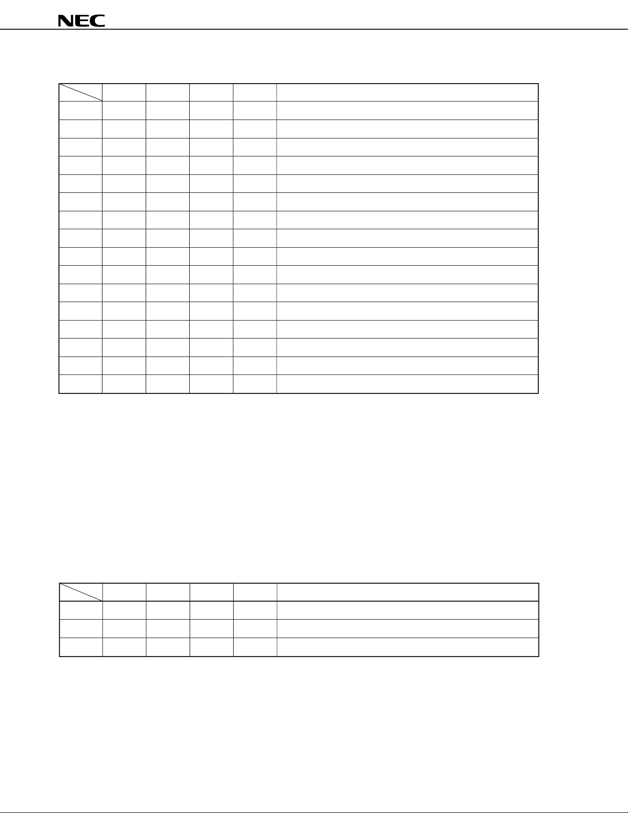
Table 2-3 Meanings of the Control Bits
µ
PD72042A, 72042B
Note 1
Bit 3
0H 0 0 0 0 Read slave status (SSR)
1H 0 0 0 1 Undefined
2H 0 0 1 0 Undefined
3H 0 0 1 1 Read data and locking
4H 0 1 0 0 Read lock address (low-order 8 bits)
5H 0 1 0 1 Read lock address (high-order 4 bits)
6H 0 1 1 0 Read slave status (SSR) and unlocking
7H 0 1 1 1 Read data
8H 1 0 0 0 Undefined
9H 1 0 0 1 Undefined
AH 1 0 1 0 Write command and locking
BH 1 0 1 1 Write data and locking
CH 1 1 0 0 Undefined
DH 1 1 0 1 Undefined
EH 1 1 1 0 Write command
FH 1 1 1 1 Write data
Bit 2 Bit 1 Bit 0 Function
Note 2
Notes 1. The transfer direction of the data-length bits of the subsequent data-length field and data in the data
field changes according to the value of bit 3 (MSB).
When bit 3 is 1: Transfer from the master unit to the slave unit
When bit 3 is 0: Transfer from the slave unit to the master unit
2. The values of control bits 3H, 6H, AH, and BH specify locking and unlocking. When an undefined value,
1H, 2H, 8H, 9H, CH, or DH, is transmitted, no acknowledge signal is returned.
Once a unit has been locked by a master unit, the locked unit rejects the control bits received from other than the
master unit that requested the lock, unless the value of the control bits is one of the values listed in Table 2-4. Then,
the unit does not output the acknowledge bit.
Table 2-4 Control Field Acceptable to a Locked Slave Unit
Bit 3 Bit 2 Bit 1 Bit 0 Function
0H 0 0 0 0 Read slave status
4H 0 1 0 0 Read lock address (low-order 8 bits)
5H 0 1 0 1 Read lock address (high-order 4 bits)
(1) Reading the slave status (SSR) (control bits: 0H, 6H)
A master unit can read the slave status (0H, 6H) to determine why the slave unit did not return the acknowledge
bit (ACK).
The slave status is determined from the result of the communication last performed by the slave unit.
All slave units can provide slave status information.
Table 2-5 lists the slave status meanings.
18
DATA SHEET S13990EJ2V0DS00
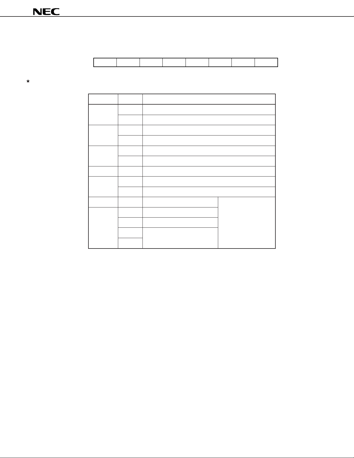
Fig. 2-2 Slave Status (SSR) Bit Format
µ
PD72042A, 72042B
MSB
bit 7 bit 6 bit 5 bit 4 bit 3 bit 2 bit 1 bit 0
Table 2-5 Slave Status Meanings
Bit Value Meaning
Note 1
Bit 0
Note 2
Bit 1
Bit 2 0 The unit is not locked.
Bit 3 0 Fixed at 0
Note 3
Bit 4
Bit 5 0 Fixed at 0
Bit 7 00 Mode 0
Bit 6 01 Mode 1
0 The slave transmission buffer is empty.
1 The slave transmission buffer is not empty.
0 The slave reception buffer is empty.
1 The slave reception buffer is not empty.
1 The unit is locked.
0 Slave transmission disabled
1 Slave transmission enabled
Indicates the highest
mode supported by the
Note 4
unit
.
LSB
10 Reserved for future expansion
11
Notes 1. The slave transmission buffer is accessed during a data read operation (control bits: 3H, 7H).
For the µPD72042A and µPD72042B, this buffer corresponds to the TBF available when STRQ of the
FLG register is set to 1.
2. The slave reception buffer is accessed during a data write operation (control bits: 8H, AH, BH, EH, FH).
µ
For the
PD72042A and µPD72042B, this buffer corresponds to the RBF available when SLRE of the
FLG register is set to 1.
3. The value of bit 4 can be selected by using the UAR1 register.
µ
4. Bits 7 and 6 are currently fixed to 10 in the hardware of the
PD72042A and µPD72042B.
(2) Data/command transfer (control bits: Read (3H, 7H), write (AH, BH, EH, FH))
When data read (3H, 7H) is set, the data in the data buffer of the slave unit is read into the master unit.
When data write (BH, FH) or command write (AH, EH) is set, the data received by the slave unit is processed
according to the operation specifications for the slave unit.
Remarks 1. The user can select data and commands as necessary according to the system.
2. 3H, AH, and BH may cause locking, depending on the communication conditions and status.
DATA SHEET S13990EJ2V0DS00
19
µ
PD72042A, 72042B
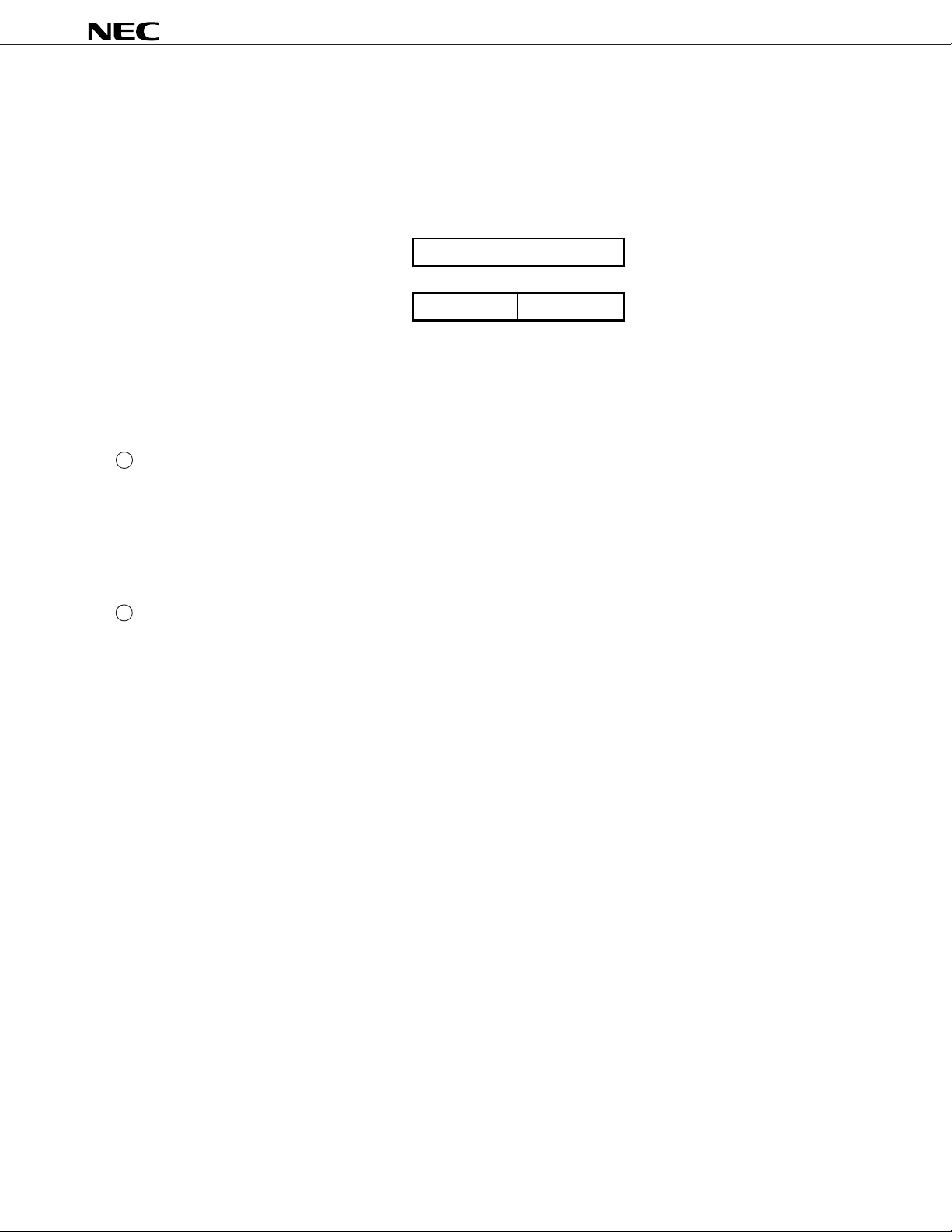
(3) Reading a lock address (control bits: 4H, 5H)
When a lock address read operation (4H, 5H) is specified, the address (12 bits) of the master unit that
issued the lock instruction is read in one-byte form, as shown below.
Fig. 2-3 Lock Address Format
MSB LSB
Control bits : 4H
Control bits : 5H
(4) Locking and unlocking (control bits: Locking (3H, AH, BH), unlocking (6H))
The lock function is used to enable the transfer a message using more than one communication frame.
When locked, a unit cannot receive data from other than the unit that requested the lock.
Locking and unlocking are performed as follows:
1 Locking
The master unit can lock the slave unit by specifying the lock with the corresponding control bits (3H, AH,
BH). In this case, when the transmission or reception of acknowledge bit 0 for the data-length field has been
completed, but the communication frame is then terminated before transmission or reception of as many data
bytes as are specified by the data-length bits is completed, the slave unit is locked. At this time, the bit
indicating the lock status (bit 2) in the slave status byte is set to 1.
2 Unlocking
The master unit can unlock a locked slave unit when the control bits specify locking (3H, AH, or BH) or
unlocking (6H). The slave unit is unlocked once as many data bytes as are specified by the data-length bits
have been transmitted or received within one communication frame. At this time, the bit indicating the lock
status (bit 2) in the slave status byte is reset to 0.
For broadcast, locking or unlocking is not performed.
Low-order 8 bits
Undefined High-order 4 bits
Caution When a locked unit is to be unlocked by the unit itself, hardware reset or software reset must
be performed. (The lock status can be checked by referring to the contents of the LOR2 register.)
20
DATA SHEET S13990EJ2V0DS00
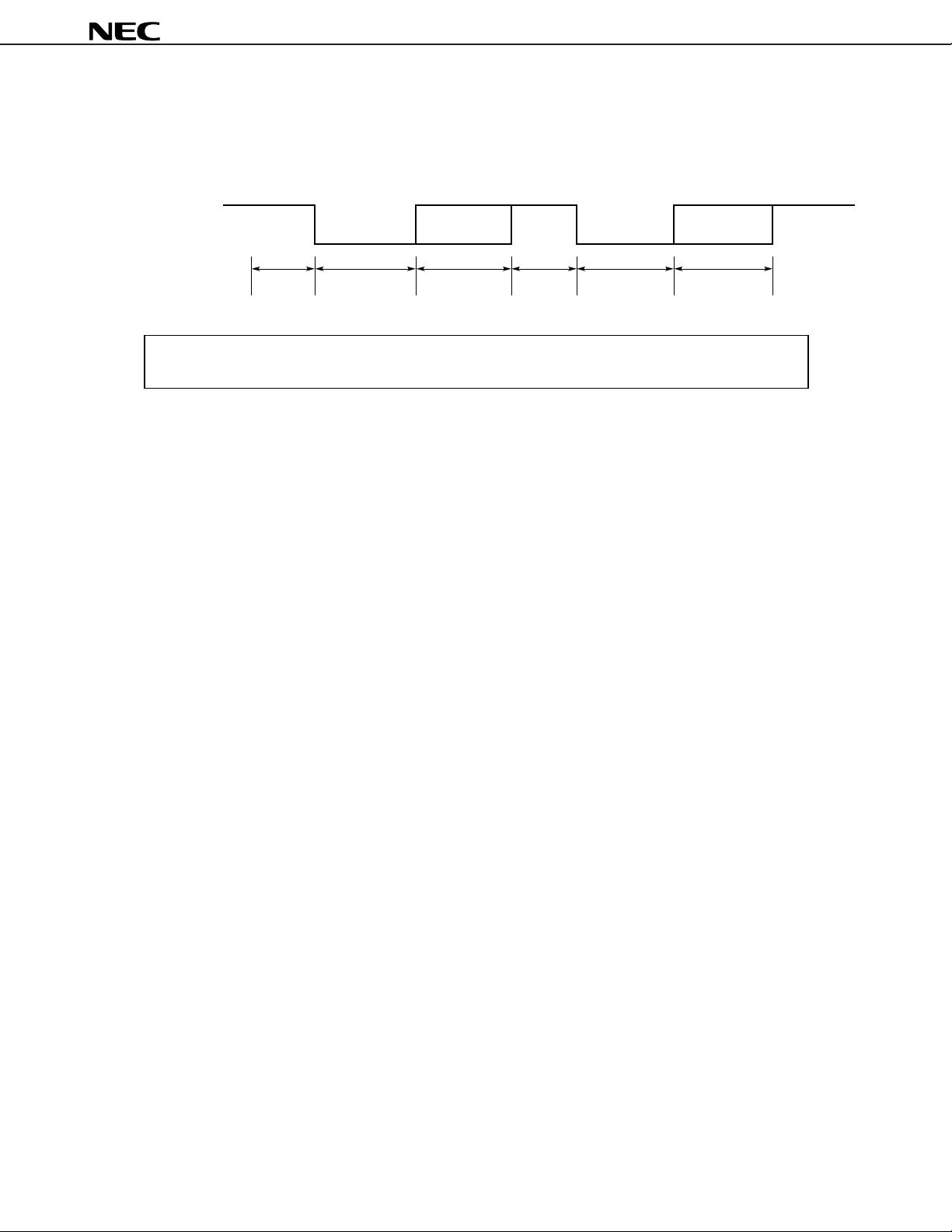
2.5 BIT FORMAT
Fig. 2-4 illustrates the bits that constitute an IEBus communication frame.
Fig. 2-4 IEBus Bit Format (Concept)
Logic "1"
Logic "0"
µ
PD72042A, 72042B
Preparation
period
Logic 1: The potential difference between the bus lines (the BUS+ and BUS- pins) is 20 mV or less (low level).
Logic 0: The potential difference between the bus lines (the BUS+ and BUS- pins) is 120 mV or more (high level).
Synchronization
period
Data period
Preparation
period
Synchronization
period
Data period
Preparation period : First and subsequent low-level (logic 1) periods
Synchronization period : Next high-level (logic 0) period
Data period : Period in which a bit value is indicated (logic 1 = low level, logic 0 = high level)
The synchronization and data periods are almost equal in duration.
For the IEBus, synchronization is established for each bit. The specifications of the total time required for a bit
and the duration of each period allotted within the bit vary depending on the type of the transmission bits, and whether
the unit is a master or slave.
DATA SHEET S13990EJ2V0DS00
21

µ
PD72042A, 72042B
3. MICROCOMPUTER INTERFACE
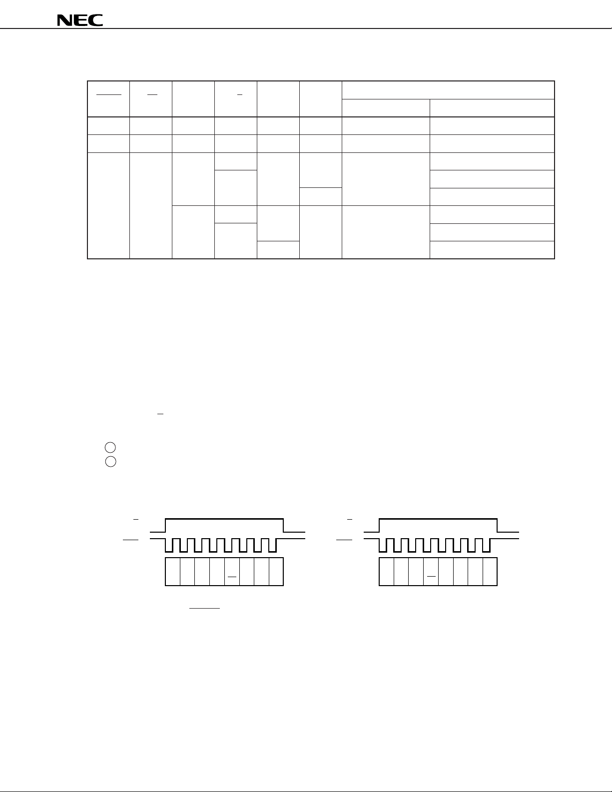
3.1 TRANSFER METHOD
Either of two microcomputer interface modes can be selected: three-wire serial I/O mode or two-wire serial I/O
mode.
Whether three-wire serial I/O mode or two-wire serial I/O mode is selected depends on the input level of the SEL
pin (pin 12). (See Section 3.3 for details.)
SEL ← 1: Three-wire serial I/O
SEL ← 0: Two-wire serial I/O
(1) Three-wire serial I/O (SEL ← 1)
Three wires are used to read and write data. The three wires are the serial clock input (SCK), serial data input
Note 1
(SI
(a) Read operation
), and serial data output (SO
Data is output to the SO pin upon detecting the falling edge of the SCK pin.
Note 2
).
(b) Write operation
Data is input via the SI pin upon detecting the rising edge of the SCK pin. At this time, 1 is output on the
SO pin.
(2) Two-wire serial I/O (SEL ← 0)
Two wires are used to read and write data. The two wires are the serial clock input (SCK) and serial data I/O
Note 1
(SIO
(a) Read operation
(b) Write operation
Notes 1. The SI pin for three-wire serial I/O mode is also used as the SIO pin for two-wire serial I/O mode.
).
The SIO pin is placed in the output state, and data is output upon detecting the falling edge of the SCK pin.
The SIO pin is placed in the input state, and data is input upon detecting the rising edge of the SCK pin.
2. The impedance of the SO pin for three-wire serial I/O mode goes high in two-wire serial I/O mode. So,
connect the SO pin to GND or V
DD.
22
DATA SHEET S13990EJ2V0DS00
µ
Table 3-1 I/O States of the SIO (SI) and SO Pins
PD72042A, 72042B
RESET CS SEL C/D SI (SIO) SO
Three-wire/two-wire Operating mode
0 ×××I Hi-Z – Reset state
11×× I Hi-Z – Chip nonselected state
1 0 1 1 I O* Three-wire Control mode
0 Data write mode
O Data read mode
0 1 I Hi-Z Two-wire Control mode
0 Data write mode
O Data read mode
State
I : Input state Hi-Z : High-impedance state
O : Output state × : Don’t care
O* : State in which 1 is output
3.2 DATA TRANSFER FORMAT
3.2.1 Three-Wire Data Transfer (SEL = 1)
(1) Control mode
When the C/D input is set high, control mode is set to control data transfer. Data transfer control involves the
following processing.
1 Register address setting
2 Register read/write selection
µ
PD72042A (starting with MSB) (b) µPD72042B (starting with LSB)
(a)
C/D
SCK
SI
A3 A2 A1 A0
R
×××
/
W
C/D
SCK
SI
×××
R
/
W
A3A2A1A0
Remark After reset (RESET) cancellation, the state enabling writing to the register at address 0000B is set.
Caution In control mode, each data item is read every eighth clock pulse. (Data of less than eight clock
periods is ignored.)
DATA SHEET S13990EJ2V0DS00
23
µ
PD72042A, 72042B
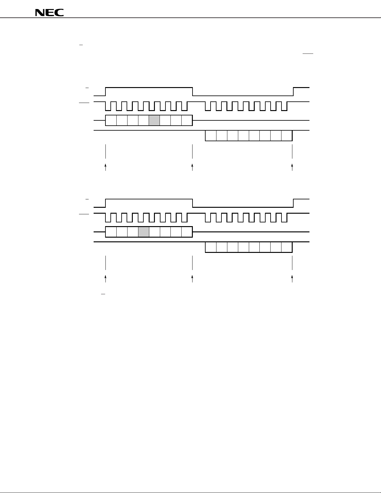
(2) Data read mode
When the C/D pin is set low after register read is selected in control mode, the data read mode is set. In data
read mode, the data in a read register is read on the SO pin upon detecting the falling edge of the SCK pin.
µ
PD72042A (starting with MSB)
(a)
C/D
SCK
SI
SO
State
Serial clock counter
reset pointer
A3 A2 A1 A0 ×××
“1”
Control mode
(selection of register read)
1
D7 D6 D5 D4 D3 D2 D1 D0
Data read mode
(b)µPD72042B (starting with LSB)
C/D
SCK
1
SI
SO
State
Serial clock counter
reset pointer
“1”
(selection of register read)
A0 A1 A2 A3×××
D0 D1 D2 D3 D4 D5 D6 D7
Control mode
Data read mode
Caution When the C/D pin is set high in data read mode, the serial clock counter is reset. Therefore, the
remaining bits of the byte cannot be read; at the next falling edge, read is performed starting from
the next byte in the case of RBF, or from the first bit for other registers.
24
DATA SHEET S13990EJ2V0DS00
µ
PD72042A, 72042B
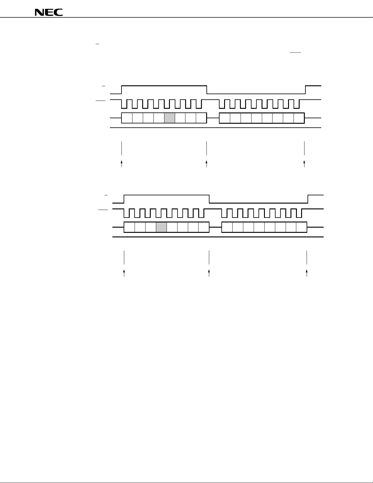
(3) Data write mode
When the C/D pin is set low after register write has been selected in control mode, data write mode is set. In
data write mode, data for a write register is applied to the SI pin at the rising edge of the SCK pin.
µ
PD72042A (starting with MSB)
(a)
C/D
SCK
SI
SO
State
Serial clock counter
reset pointer
A3 A2 A1 A0 ×××
“1”
Control mode
(selection of register write)
0
D7 D6 D5 D4 D3 D2 D1 D0
Data write mode
(b)µPD72042B (starting with LSB)
C/D
SCK
A0 A1 A2 A3×××
SI
SO
State
Serial clock counter
reset pointer
0
“1”
Control mode
(selection of register write)
D0 D1 D2 D3 D4 D5 D6 D7
Data write mode
Caution Register overwrite is started immediately after the eighth clock rising edge. All registers other
than TBF are overwritten on the eighth clock rising edge. (Data of less than eight clock periods
is ignored.)
DATA SHEET S13990EJ2V0DS00
25
µ
PD72042A, 72042B
3.2.2 Two-Wire Data Transfer (SEL = 0)
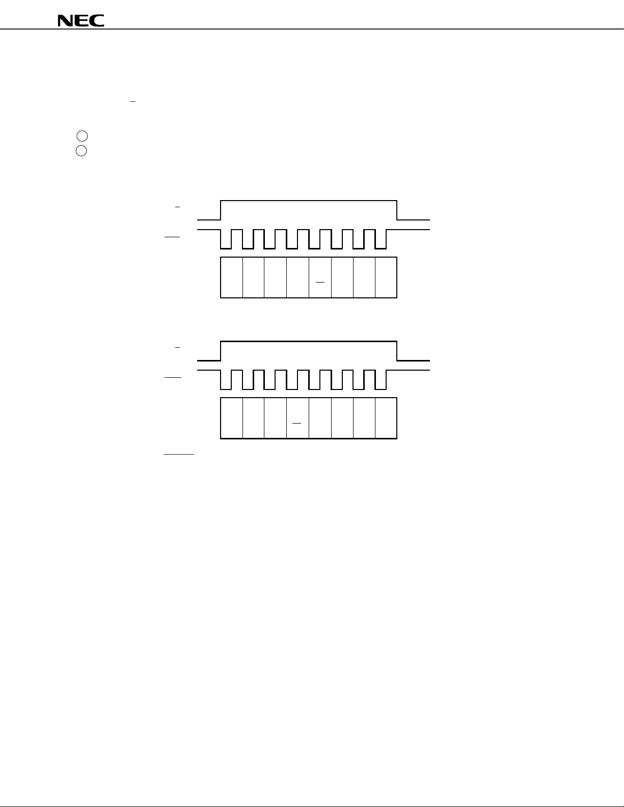
(1) Control mode
When the C/D input is set high, control mode is set to control data transfer. Data transfer control involves the
following processing.
1 Register address setting
2 Register read/write selection
µ
PD72042A (starting with MSB)
(a)
C/D
SCK
R
SIO
A3 A2 A1 A0
/
×××
W
(b) µPD72042B (starting with LSB)
C/D
SCK
R
SIO
××× A0 A1 A2 A3
/
W
Remark After reset (RESET) cancellation, the state enabling writing to the register at address 0000B is set.
Caution In control mode, each data item is read every eighth clock pulse. (Data of less than eight clock
periods is ignored.)
26
DATA SHEET S13990EJ2V0DS00
(2) Data read mode
(a)µPD72042A (starting with MSB)
C/D
SCK
µ
PD72042A, 72042B
Note
SIO
State
Serial clock counter
reset pointer
A3 A2 A1 A0 ×××
(selection of register read)
(b)µPD72042B (starting with LSB)
C/D
SCK
Note
SIO
State
Serial clock counter
reset pointer
(selection of register read)
Note SIO pin input state
SIO pin output state
1
Control mode
A0 A1 A2
1××× A3
Control mode
D7 D6 D5 D4 D3 D2 D1 D0
Data read mode
D0 D1 D2 D3 D4 D5 D6 D7
Data read mode
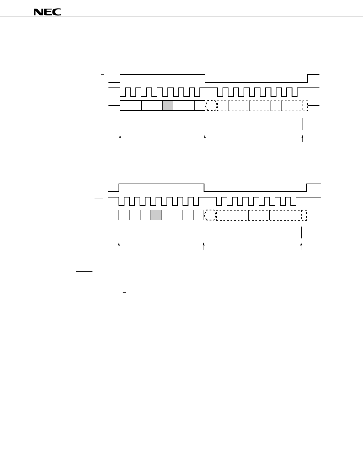
Cautions 1. When the C/D pin is set high in data read mode, the serial clock counter is reset. Therefore,
the remaining bits of the byte cannot be read; at the next falling edge, a read operation is
performed starting from the next byte in the case of RBF, or from the first bit for other registers.
2. The SIO pin is a CMOS I/O pin. So, be careful to avoid an output collision between the SIO
pin and the microcomputer. Further, a pull-up resistor is required when N-ch open-drain
output of the microcomputer is used. Note that if the last output level is low upon the
termination of read mode, current will flow constantly.
DATA SHEET S13990EJ2V0DS00
27
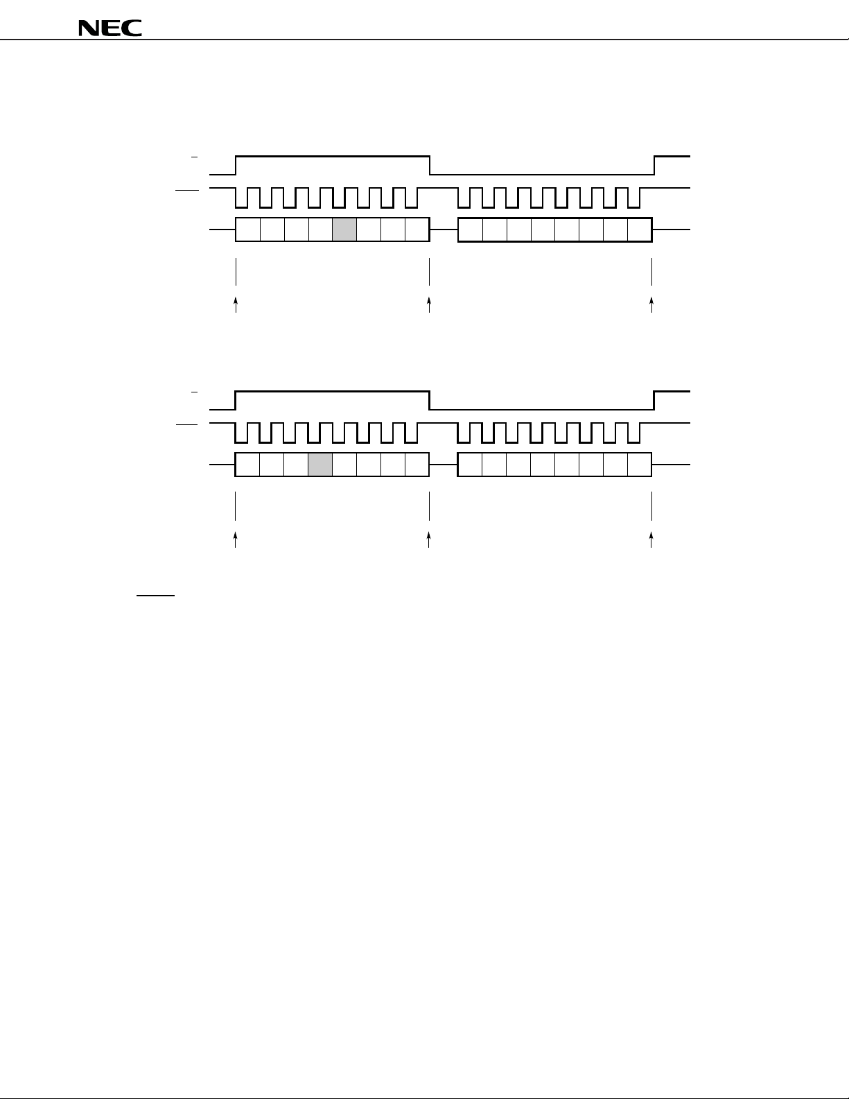
(3) Data write mode
(a)µPD72042A (starting with MSB)
C/D
SCK
µ
PD72042A, 72042B
Note
SIO
State
Serial clock counter
reset pointer
A3 A2 A1 A0 ×××
(selection of register write)
(b)µPD72042B (starting with LSB)
C/D
SCK
Note
SIO
State Data write mode
Serial clock counter
reset pointer
(selection of register write)
Note SIO pin input state
0
Control mode
A0 A1 A2 A3×××
0
Control mode
D7 D6 D5 D4 D3 D2 D1 D0
Date write mode
D0 D1 D2 D3 D4 D5 D6 D7
Caution Register overwrite is started immediately after the eighth clock rising edge. All registers other
than TBF are overwritten at the eighth clock rising edge. (Data of less than eight clock periods
is ignored.)
28
DATA SHEET S13990EJ2V0DS00
 Loading...