NEC UPD70F3102GJ-33-8EU Datasheet

PRELIMINARY DATA SHEET
MOS INTEGRATED CIRCUITS
µµµµ
PD70F3102-33
V850E/MS1
TM
32-/16-BIT SINGLE-CHIP MICROCONTROLLER
The µPD70F3102-33 is a product that substitutes the internal mask ROM of the µPD703102-33 with flash
memory. This enables users to perform on-board program writing and erasure, enabling effective evaluation during
system development, small-lot production of multiple devices, and rapid production start, and quick development and
time-to-market.
A version using a 3.3 V power supply for external pins, the µPD70F3102-A33, is also available.
For additional information, refer to the following user’s manuals. Be sure to read them before starting
design.
V850E/MS1 User’s Manual Hardware: U12688E
V850E/MS1 User’s Manual Architecture: U12197E
FEATURES
PD703102-33 compatible
•
µ
Can be replaced by the µPD703102-33 with internal mask ROM for mass production
Internal flash memory: 128 KB
•
ORDERING INFORMATION
Part Number Package
PD70F3102GJ-33-8EU 144-pin plastic LQFP (fine pitch) (20 × 20)
µ
PD70F3102GJ-33-UEN 144-pin plastic LQFP (fine pitch) (20 × 20)
µ
The information contained in this document is being issued in advance of the production cycle for the
device. The parameters for the device may change before final production or NEC Corporation, at its own
discretion, may withdraw the device prior to its production.
Not all devices/types available in every country. Please check with local NEC representative for
availability and additional information.
Document No. U13844EJ2V0DS00 (2nd edition)
Date Published July 2000 N CP(K)
Printed in Japan
The mark shows major revised points.
©
1999
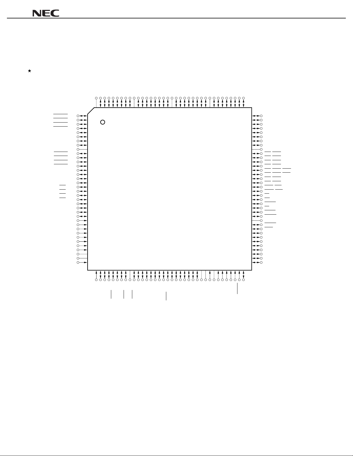
PIN CONFIGURATION (Top View)
µµµµ
PD70F3102-33
144-pin plastic LQFP (fine pitch) (20
PD70F3102GJ-33-8EU
•
µµµµ
PD70F3102GJ-33-UEN
•
µµµµ
DD
V
D0/P40
D1/P41
D2/P42
D3/P43
144
143
142
141
INTP103/DMARQ3/P07
INTP102/DMARQ2/P06
INTP101/DMARQ1/P05
INTP100/DMARQ0/P04
INTP113/DMAAK3/P17
INTP112/DMAAK2/P16
INTP111/DMAAK1/P15
INTP110/DMAAK0/P14
TI10/P03
TCLR10/P02
TO101/P01
TO100/P00
V
TI11/P13
TCLR11/P12
TO111/P11
TO110/P10
INTP123/TC3/P107
INTP122/TC2/P106
INTP121/TC1/P105
INTP120/TC0/P104
TI12/P103
TCLR12/P102
TO121/P101
TO120/P100
ANI7/P77
ANI6/P76
ANI5/P75
ANI4/P74
ANI3/P73
ANI2/P72
ANI1/P71
ANI0/P70
AV
AV
AV
1
2
3
4
5
6
7
8
SS
9
10
11
12
13
14
15
16
17
18
19
20
21
22
23
24
25
26
27
28
29
30
31
32
33
DD
34
SS
REF
35
36
140
3738394041424344454647484950515253545556575859606162636465666768697071
××××
D4/P44
D5/P45
139
138
20)
D6/P46
137
D7/P47
VSSD8/P50
136
135
134
D9/P51
D10/P52
133
132
D11/P53
D12/P54
D13/P55
131
130
129
D14/P56
D15/P57
HVDDA0/PA0
128
127
126
125
A1/PA1
A2/PA2
124
123
A3/PA3
A4/PA4
122
121
A5/PA5
A6/PA6
120
119
A7/PA7
VSSA8/PB0
118
117
116
A9/PB1
A10/PB2
115
114
A11/PB3
A12/PB4
A13/PB5
113
112
111
A14/PB6
A15/PB7
110
109
108
107
106
105
104
103
102
101
100
99
98
97
96
95
94
93
92
91
90
89
88
87
86
85
84
83
82
81
80
79
78
77
76
75
74
73
72
A16/P60
A17/P61
A18/P62
A19/P63
A20/P64
A21/P65
A22/P66
A23/P67
HV
DD
CS0/RAS0/P80
CS1/RAS1/P81
CS2/RAS2/P82
CS3/RAS3/P83
CS4/RAS4/IOWR/P84
CS5/RAS5/IORD/P85
CS6/RAS6/P86
CS7/RAS7/P87
LCAS/LWR/P90
UCAS/UWR/P91
RD/P92
WE/P93
BCYST/P94
OE/P95
HLDAK/P96
HLDRQ/P97
SS
V
REFRQ/PX5
WAIT/PX6
CLKOUT/PX7
TO150/P120
TO151/P121
TCLR15/P122
TI15/P123
INTP150/P124
INTP151/P125
INTP152/P126
DD
P21
NMI/P20
RXD0/SI0/P23
TXD0/SO0/P22
2
V
SCK0/P24
SCK1/P27
RXD1/SI1/P26
TXD1/SO1/P25
TI13/P33
TO131/P31
TCLR13/P32
INTP130/P34
INTP132/SI2/P36
INTP131/SO2/P35
INTP133/SCK2/P37
TO130/P30
INTP142/SI3/P116
INTP143/SCK3/P117
Preliminary Data Sheet U13844EJ2V0DS00
TI14/P113
TO141/P111
TCLR14/P112
INTP140/P114
INTP141/SO3/P115
DD
X2
X1
CV
TO140/P110
SS
CV
CKSEL
MODE0
MODE1
MODE2
PP
RESET
MODE3/V
INTP153/ADTRG/P127

µµµµ
PD70F3102-33
PIN IDENTIFICATION
A0 to A23: Address Bus P50 to P57: Port 5
ADTRG: AD Trigger Input P60 to P67: Port 6
ANI0 to ANI7: Analog Input P70 to P77: Port 7
DD:
AV
REF
AV
: Analog Reference Voltage P90 to P97: Port 9
AVSS: Analog Ground P100 to P107: Port 10
BCYST: Bus Cycle Start Timing P110 to P117: Port 11
CKSEL:
CLKOUT: Clock Output PB0 to PB7: Port B
CS0 to CS7: Chip Select PX5 to PX7: Port X
CVDD: Clock Generator Power Supply RAS0 to RAS7: Row Address Strobe
CVSS: Clock Generator RD: Read
D0 to D15: Data Bus REFRQ: Refresh Request
DMAAK0 to DMAAK3: DMA Acknowledge RESET: Reset
DMARQ0 to DMARQ3: DMA Request RXD0, RXD1: Receive Data
HLDAK: Hold Acknowledge SCK0 to SCK3: Serial Clock
HLDRQ: Hold Request SI0 to SI3: Serial Input
HVDD: Power Supply for External Pins SO0 to SO3: Serial Output
INTP100 to INTP103, TC0 to TC3: Terminal Count Signal
INTP110 to INTP113, TCLR10 to TCLR15: Timer Clear
INTP120 to INTP123, TI10 to TI15: Timer Input
INTP130 to INTP133, TO100, TO101,
INTP140 to INTP143, TO110, TO111,
INTP150 to INTP153: Interrupt Request from Peripherals TO120, TO121,
IORD: I/O Read Strobe TO130, TO131,
IOWR: I/O Write Strobe TO140, TO141,
LCAS: Lower Column Address Strobe TO150, TO151: Timer Output
LWR: Lower Write Strobe TXD0, TXD1: Transmit Data
MODE0 to MODE3: Mode UCAS: Upper Column Address Strobe
NMI: Non-Maskable Interrupt Request UWR: Upper Write Strobe
OE: Output Enable VDD: Power Supply for Internal Unit
P00 to P07: Port 0 VPP: Programming Power Supply
P10 to P17: Port 1 VSS: Ground
P20 to P27: Port 2 WAIT: Wait
P30 to P37: Port 3 WE: Write Enable
P40 to P47: Port 4 X1, X2: Crystal
Analog Power Supply P80 to P87: Port 8
Clock Generator Operating Mode
Select
P120 to P127: Port 12
PA0 to PA7: Port A
Preliminary Data Sheet U13844EJ2V0DS00
3
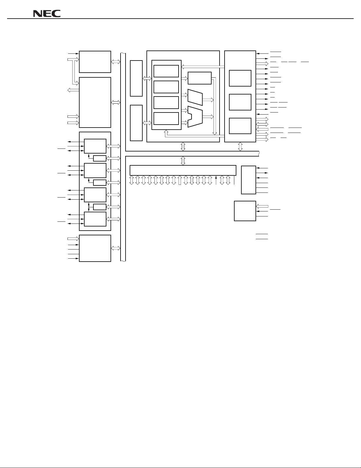
INTERNAL BLOCK DIAGRAM
µµµµ
PD70F3102-33
INTP100 to INTP103,
INTP110 to INTP113,
INTP120 to INTP123,
INTP130 to INTP133,
INTP140 to INTP143,
INTP150 to INTP153
TCLR10 to TCLR15
NMI
TO100, TO101,
TO110, TO111,
TO120, TO121,
TO130, TO131,
TO140, TO141,
TO150, TO151
TI10 to TI15
SO0/TXD0
SI0/RXD0
SCK0
SO1/TXD1
SI1/RXD1
SCK1
SO2
SI2
SCK2
SO3
SI3
SCK3
INTC
RPU
SIO
UART0/CSI0
BRG0
UART1/CSI1
BRG1
CSI2
BRG2
CSI3
Flash memory
128 KB
RAM
4 KB
PX5 to PX7
PB0 to PB7
Instruction queue
System registers
General-purpose
registers
(32 bits × 32)
PA0 to PA7
P120 to P127
P110 to P117
PC
P90 to P97
P80 to P87
P100 to P107
Multiplier
(32 × 32 → 64)
Port
P70 to P77
P60 to P67
Barrel
shifter
ALU
P50 to P57
P40 to P47
P30 to P37
P21 to P27
P20
DRAMC
Page ROM
controller
P10 to P17
P00 to P07
BCUCPU
DMAC
DD
HV
System
controller
CG
HLDRQ
HLDAK
CS0 to CS7/RAS0 to RAS7
IOWR
IORD
REFRQ
BCYST
WE
RD
OE
UWR/UCAS
LWR/LCAS
WAIT
A0 to A23
D0 to D15
DMARQ0 to DMARQ3
DMAAK0 to DMAAK3
TC0 to TC3
CKSEL
CLKOUT
X1
X2
CV
DD
CV
SS
MODE0 to MODE3
RESET
V
PP
ANI0 to ANI7
AV
AV
AV
ADTRG
V
DD
V
REF
SS
DD
ADC
SS
4
Preliminary Data Sheet U13844EJ2V0DS00

µµµµ
PD70F3102-33
CONTENTS
1. DIFFERENCES AMONG PRODUCTS .............................................................................................. 6
1.1 Differences Between
1.2 Differences Between
2. PIN FUNCTIONS................................................................................................................................. 7
2.1 Port Pins ...................................................................................................................................... 7
2.2 Non-Port Pins .............................................................................................................................. 10
2.3 Pin I/O Circuit Types and Recommended Connection of Unused Pins ................................ 14
3. FLASH MEMORY PROGRAMMING ................................................................................................. 17
3.1 Selection of Communication System........................................................................................ 17
3.2 Flash Memory Programming Functions ................................................................................... 18
3.3 Connecting the Dedicated Flash Programmer......................................................................... 18
4. ELECTRICAL SPECIFICATIONS....................................................................................................... 19
4.1 Normal Operation Mode ............................................................................................................. 19
4.2 Flash Memory Programming Mode ........................................................................................... 74
PD70F3102-33 and
µµµµ
PD70F3102-33 and
µµµµ
PD703102-33 ...................................................... 6
µµµµ
PD70F3102A-33.................................................. 6
µµµµ
5. PACKAGE DRAWINGS...................................................................................................................... 76
6. RECOMMENDED SOLDERING CONDITIONS................................................................................. 78
Preliminary Data Sheet U13844EJ2V0DS00
5
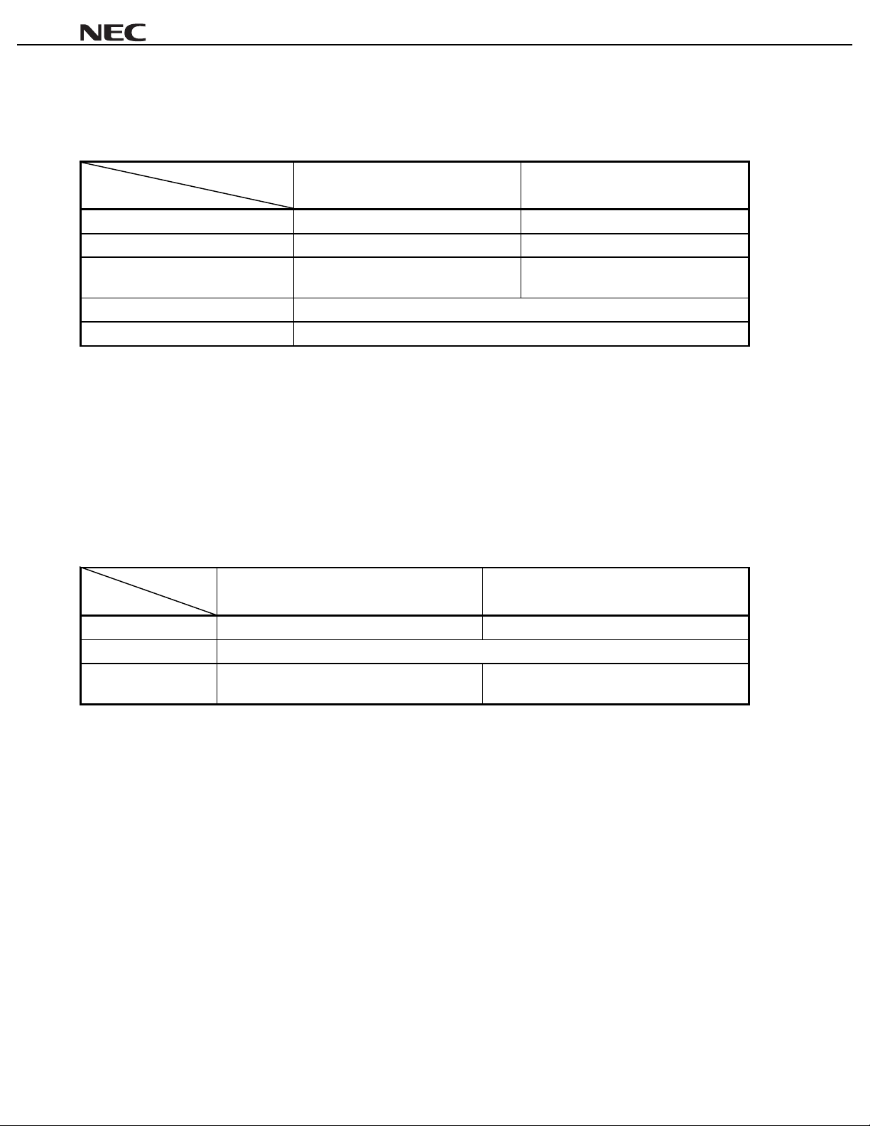
1. DIFFERENCES AMONG PRODUCTS
µµµµ
PD70F3102-33
1.1 Differences Between
Item
Internal ROM Flash memory Mask ROM
Flash memory programming pin Provided (VPP) None
Flash memory programming mode Prov i ded (MODE0 = L, MODE1 = H,
Electrical speci fications Consumption current etc. differ (see individual data sheets).
Others Circuit scale and mast er l ayout differ, thus nois e i m m uni ty, noise radiation, etc. differ.
PD70F3102-33 and
µµµµ
Product
MODE2 = L, MODE3/V
PD703102-33
µµµµ
PD70F3102-33
µ
PP
= 7.8 V)
None
PD703102-33
µ
Cautions 1. There are differences in noise immunity and noise radiation between the flash memory
version and mask ROM version. When pre-producing an application set with the flash
memory version and then mass-producing it with the mask ROM version, be sure to conduct
sufficient evaluation for commercial samples (not engineering samples) of the mask ROM
version.
2. When switching from the flash memory version to the mask ROM version, write the same
code to the free area of the internal ROM.
1.2 Differences Between
PD70F3102-33 and
µµµµ
PD70F3102A-33
µµµµ
Product
Item
DD
HV
Electrical speci fications See individual data sheets .
Package • 144-pin plastic LQFP (fine pitch) (20 × 20) • 157-pin plastic FBGA (14 × 14)
4.5 to 5.5 V 3.0 to 3.6 V
PD70F3102-33
µ
PD70F3102A-33
µ
• 144-pin plastic LQFP (fine pitch) (20 × 20)
6
Preliminary Data Sheet U13844EJ2V0DS00
µµµµ
PD70F3102-33
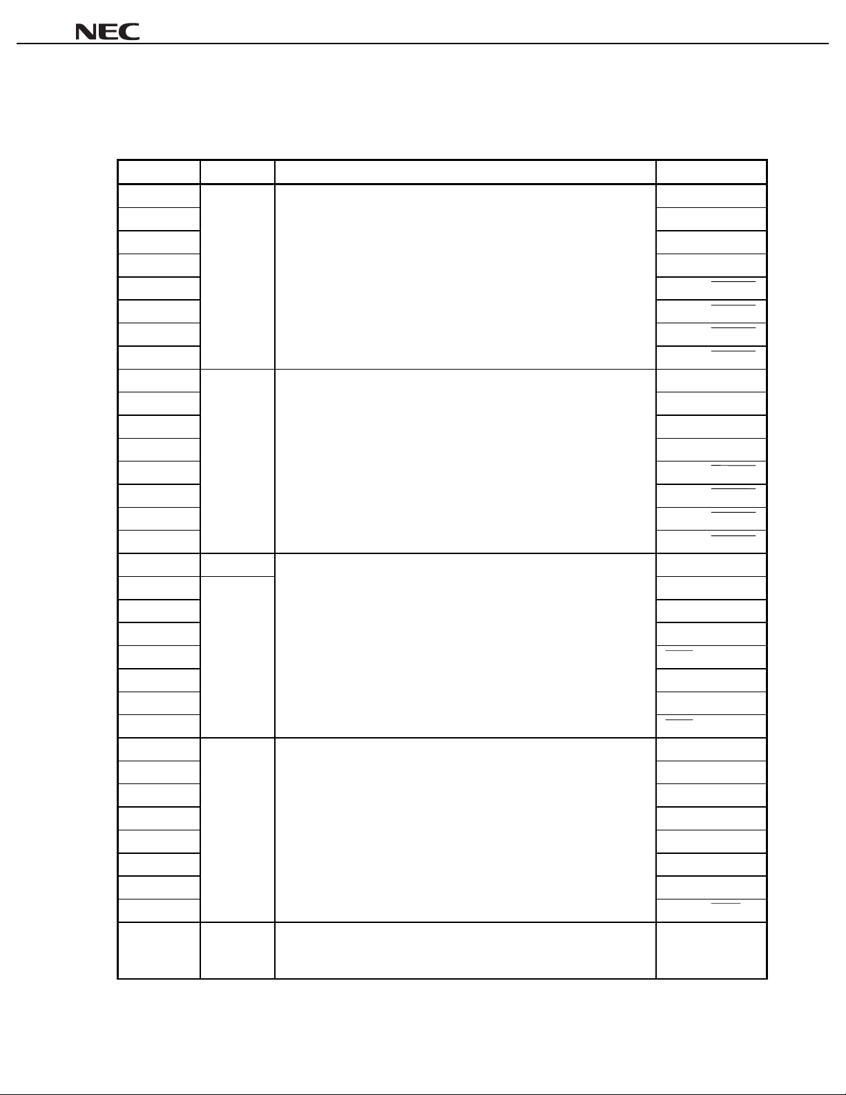
2. PIN FUNCTIONS
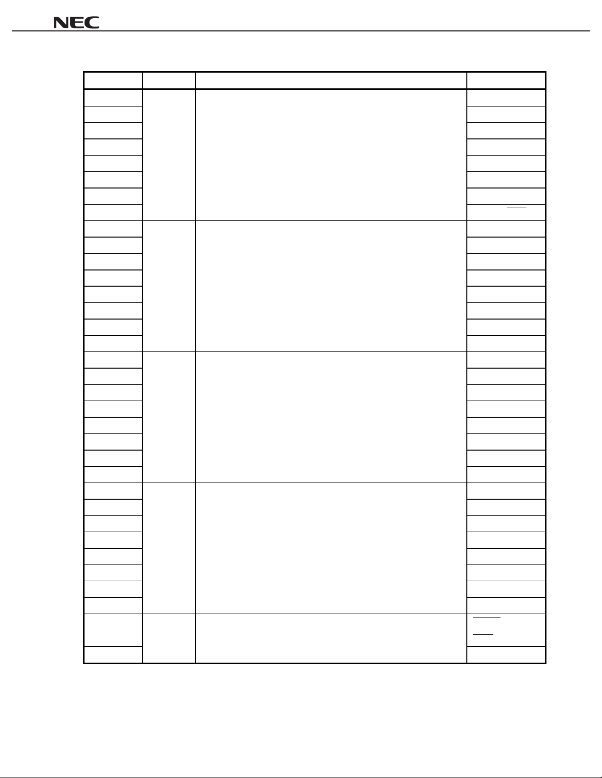
2.1 Port Pins
Pin Name I/O Function Alternate Function
(1/3)
P00 TO100
P01 TO101
P02 TCLR10
P03 TI10
P04 INTP100/DMARQ0
P05 INTP101/DMARQ1
P06 INTP102/DMARQ2
P07
P10 TO110
P11 TO111
P12 TCLR11
P13 TI11
P14 INTP110/DMAAK0
P15 INTP111/DMAAK1
P16 INTP112/DMAAK2
P17
P20 Input NMI
P21 –
P22 TXD0/SO0
P23 RXD0/SI0
P24 SCK0
P25 TXD1/SO1
P26 RXD1/SI1
P27
P30 TO130
P31 TO131
P32 TCLR13
P33 TI13
P34 INTP130
P35 INTP131/SO2
P36 INTP132/SI2
P37
P40 to P47 I/O Port 4
I/O Port 0
8-bit I/O port
Input/output can be spec i f i ed i n 1-bi t units.
I/O Port 1
8-bit I/O port
Input/output can be spec i f i ed i n 1-bi t units.
Port 2
I/O
I/O Port 3
P20 is an input-only port.
When a valid edge is input, it operates as an NMI input. The st atus of
the NMI input is shown by bi t 0 of register P2.
P21 to P27 is a 7-bit I/O port.
Input/output can be spec i f i ed i n 1-bi t units.
8-bit I/O port
Input/output can be spec i f i ed i n 1-bi t units.
8-bit I/O port
Input/output can be spec i f i ed i n 1-bi t units.
INTP103/DMARQ3
INTP113/DMAAK3
SCK1
INTP133/SCK2
D0 to D7
Preliminary Data Sheet U13844EJ2V0DS00
7

µµµµ
PD70F3102-33
(2/3)
Pin Name I/O Function Alternate Function
P50 to P57 I/O Port 5
8-bit I/O port
Input/output can be spec i f i ed i n 1-bi t units.
P60 to P67 I/O Port 6
8-bit I/O port
Input/output can be spec i f i ed i n 1-bi t units.
P70 to P77 Input Port 7
8-bit input-only port
P80 CS0/RAS0
P81 CS1/RAS1
P82 CS2/RAS2
P83 CS3/RAS3
P84 CS4/RAS4/IOWR
P85 CS5/RAS5/IORD
P86 CS6/RAS6
P87
P90 LCAS/LWR
P91 UCAS/UWR
P92 RD
P93 WE
P94 BCYST
P95 OE
P96 HLDAK
P97
P100 TO120
P101 TO121
P102 TCLR12
P103 TI12
P104 INTP120/TC0
P105 INTP121/TC1
P106 INTP122/TC2
P107
I/O Port 8
8-bit I/O port
Input/output can be spec i f i ed i n 1-bi t units.
I/O Port 9
8-bit I/O port
Input/output can be spec i f i ed i n 1-bi t units
I/O Port 10
8-bit I/O port
Input/output can be spec i f i ed i n 1-bi t units.
D8 to D15
A16 to A23
ANI0 to ANI7
CS7/RAS7
HLDRQ
INTP123/TC3
8
Preliminary Data Sheet U13844EJ2V0DS00
µµµµ
PD70F3102-33
(3/3)
Pin Name I/O Function Alternate Function
P110 TO140
P111 TO141
P112 TCLR14
P113 TI14
P114 INTP140
P115 INTP141/SO3
P116 INTP142/SI3
P117
P120 TO150
P121 TO151
P122 TCLR15
P123 TI15
P124 INTP150
P125 INTP151
P126 INTP152
P127
PA0 A0
PA1 A1
PA2 A2
PA3 A3
PA4 A4
PA5 A5
PA6 A6
PA7
PB0 A8
PB1 A9
PB2 A10
PB3 A11
PB4 A12
PB5 A13
PB6 A14
PB7
PX5 REFRQ
PX6 WAIT
PX7
I/O Port 11
8-bit I/O port
Input/output can be spec i f i ed i n 1-bi t units.
INTP143/SCK3
I/O Port 12
8-bit I/O port
Input/output can be spec i f i ed i n 1-bi t units.
INTP153/ADTRG
I/O Port A
8-bit I/O port
Input/output can be spec i f i ed i n 1-bi t units.
A7
I/O Port B
8-bit I/O port
Input/output can be spec i f i ed i n 1-bi t units.
A15
I/O Port X
3-bit I/O port
Input/output can be spec i f i ed i n 1-bi t units.
CLKOUT
Preliminary Data Sheet U13844EJ2V0DS00
9

µµµµ
PD70F3102-33
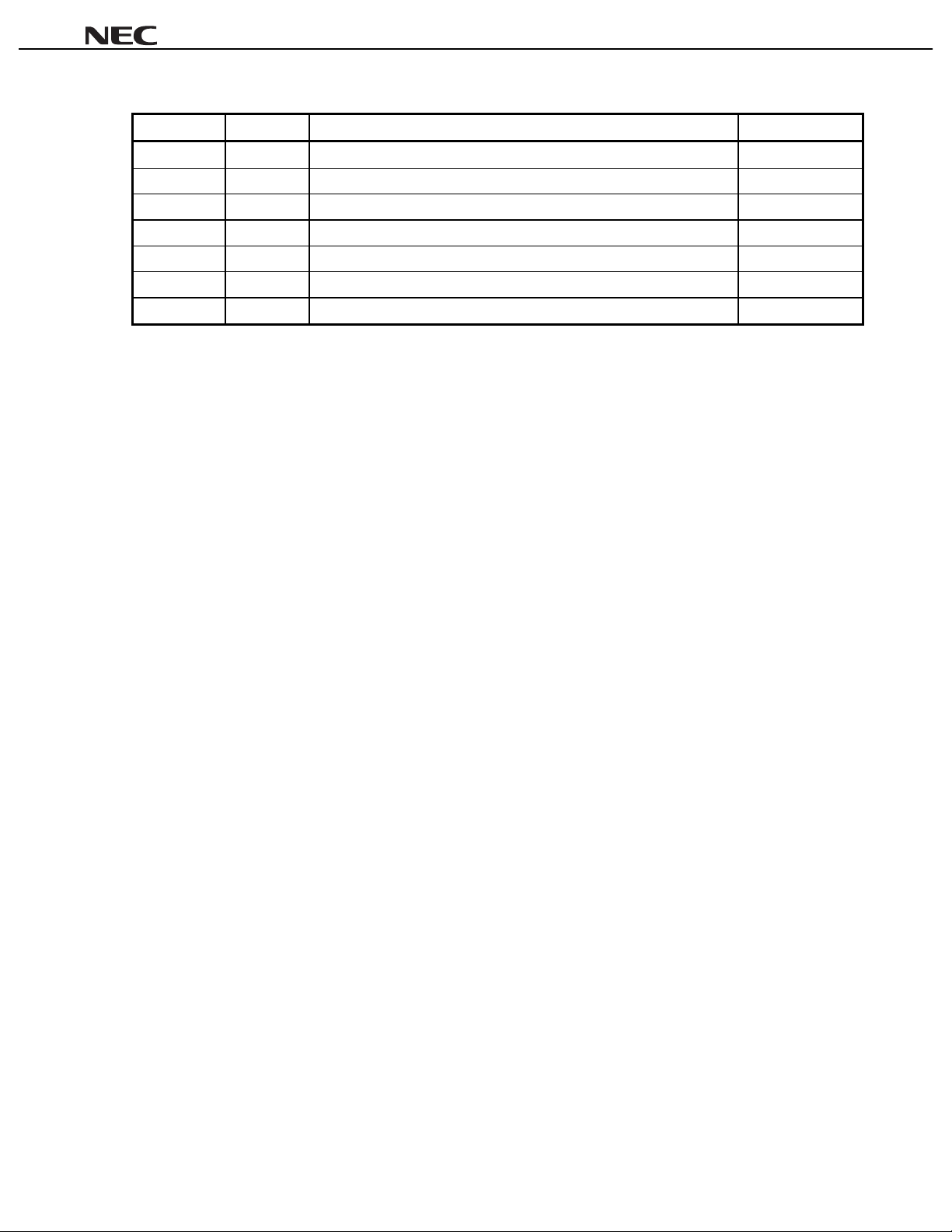
2.2 Non-Port Pins
Pin Name I/O Function Alternate Function
(1/4)
TO100 P00
TO101 P01
TO110 P10
TO111 P11
TO120 P100
TO121 P101
TO130 P30
TO131 P31
TO140 P110
TO141 P111
TO150 P120
TO151
TCLR10 P02
TCLR11 P12
TCLR12 P102
TCLR13 P32
TCLR14 P112
TCLR15
TI10 P03
TI11 P13
TI12 P103
TI13 P33
TI14 P113
TI15
INTP100 P04/DMARQ0
INTP101 P05/DMARQ1
INTP102 P06/DMARQ2
INTP103
INTP110 P14/DMAAK0
INTP111 P15/DMAAK1
INTP112 P16/DMAAK2
INTP113
INTP120 P104/TC0
INTP121 P105/TC1
INTP122 P106/TC2
INTP123
Output Pulse signal output of timers 10 to 15
P121
Input External c l ear signal input of timers 10 to 15
P122
Input External c ount clock input of tim ers 10 to 15
P123
Input External maskable interrupt request input, or timer 10 external capture
trigger input
P07/DMARQ3
Input External maskable interrupt request input, or timer 11 external capture
trigger input
P17/DMAAK3
Input External maskable interrupt request input, or timer 12 external capture
trigger input
P107/TC3
10
Preliminary Data Sheet U13844EJ2V0DS00

µµµµ
PD70F3102-33
(2/4)
Pin Name I/O Function Alternate Function
INTP130 P34
INTP131 P35/SO2
INTP132 P36/SI2
INTP133
INTP140 P114
INTP141 P115/SO3
INTP142 P116/SI3
INTP143
INTP150 P124
INTP151 P125
INTP152 P126
INTP153
SO0 P22/TXD0
SO1 P25/TXD1
SO2 P35/INTP131
SO3
SI0 P23/RXD0
SI1 P26/RXD1
SI2 P36/INTP132
SI3
SCK0 P24
SCK1 P27
SCK2 P37/INTP133
SCK3
TXD0 P22/SO0
TXD1
RXD0 P23/SI0
RXD1
D0 to D7 P40 to P47
D8 to D15
A0 to A7 PA0 to PA7
A8 to A15 PB0 to PB7
A16 to A23
LWR Output External data bus lower byte write enable signal output P90/LCAS
UWR Output External data bus upper byte write enabl e signal output P91/UCAS
RD Output External data bus read strobe signal output P92
WE Output Write enable si gnal output for DRAM P93
OE Output Output enable signal output for DRA M P95
Input External maskable interrupt request input, or timer 13 external capture
trigger input
P37/SCK2
Input External maskable interrupt request input, or timer 14 external capture
trigger input
P117/SCK3
Input External maskable interrupt request input, or timer 15 external capture
trigger input
P127/ADTRG
Output CSI0 to CSI3 serial transmission dat a out put (3-wire)
P115/INTP141
Input CSI0 to CSI 3 serial reception data input (3-wire)
P116/INTP142
I/O CSI0 to CSI3 serial clock input/output (3-wire)
P117/INTP143
Output UART0 and UART1 serial transmission data output
P25/SO1
Input UART0 and UART1 serial reception data input
P26/SI1
I/O 16-bit data bus for external memory
P50 to P57
Output 24-bit address bus for external memory
P60 to P67
Preliminary Data Sheet U13844EJ2V0DS00
11

µµµµ
PD70F3102-33
(3/4)
Pin Name I/O Function Alternate Function
LCAS Output Column address strobe signal output for lower data of DRAM P90/LWR
UCAS Output Column address strobe signal output for higher data of DRAM P91/UWR
RAS0 to RAS3 P80/CS0 to P83/CS3
RAS4 P84/CS4/IOWR
RAS5 P85/CS5/IORD
RAS6 P86/CS6
RAS7
BCYST Output Strobe signal output indicat i ng start of bus cycle P94
CS0 to CS3 P80/RAS0 to
CS4 P84/RAS4/IOWR
CS5 P85/RAS5/IORD
CS6 P86/RAS6
CS7
WAIT Input Control signal i nput that inserts a wait in the bus cycle PX6
REFRQ Output Refresh request signal output for DRA M PX5
IOWR Output DMA writ e strobe signal output P84/RAS4/CS4
IORD Output DMA read strobe signal output P85/RAS5/CS5
DMARQ0 to
DMARQ3
DMAAK0 to
DMAAK3
TC0 to TC3 Output DMA terminati on (t erminal count) signal output P104/INTP120 to
HLDAK Output Bus hold acknowledge output P96
HLDRQ Input Bus hold request i nput P97
ANI0 to ANI7 Input Analog input to A/ D converter P70 to P77
NMI Input Non-maskable interrupt request i nput P20
CLKOUT Output Syst em clock output PX7
CKSEL Input Input that spec if ies the clock generator's operation mode –
MODE0 to
MODE2
MODE3
RESET Input System reset input –
X1 Input –
X2 –
ADTRG Input A/D converter external trigger input P127/INTP153
REF
AV
DD
AV
Output Row address strobe signal output for DRAM
P87/CS7
Output Chip select signal output
P83/RAS3
P87/RAS7
Input DMA request signal input P04/INTP100 to
P07/INTP103
Output DMA acknowledge signal output P14/INTP110 to
P17/INTP113
P107/INTP123
Input Operation mode spec i f i cation
V
Connecting system clock resonator. In the case of an ex t ernal clock, it is
input to X1.
Input Reference volt age appl i ed to A/D converter –
– Positive power supply for A/D converter –
–
PP
–
12
Preliminary Data Sheet U13844EJ2V0DS00
µµµµ
PD70F3102-33
Pin Name I/O Function Alternate Function
SS
AV
CV
CV
V
HV
V
V
DD
SS
DD
DD
SS
PP
– Ground potential for A/D conv erter –
– Positive power supply for the dedicated clock generat or –
– Ground potential for dedicated cl ock generator –
– Positive power supply (i nternal unit power supply) –
– Positive power supply (external pin power supply) –
– Ground potential –
– High-voltage application pin during program write/verify MODE 3
(4/4)
Preliminary Data Sheet U13844EJ2V0DS00
13

µµµµ
PD70F3102-33
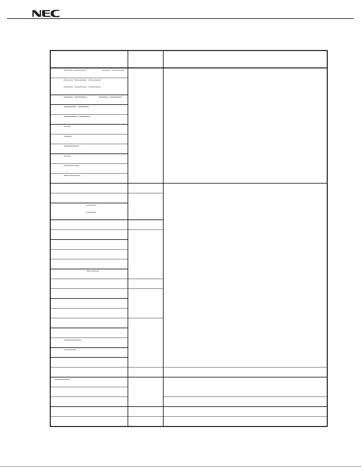
2.3 Pin I/O Circuit Types and Recommended Connection of Unused Pins
Table 2-1 shows the I/O circuit type of each pin and the recommended connection of unused pins, and Figure 2-1
shows the schematic circuit diagram for each I/O circuit type.
In the case of connection to VDD or VSS via a resistor, connection of a resistor of 1 to 10 kΩ is recommended.
Table 2-1. Pin I/O Circuit Types and Recommended Connection of Unused Pins (1/2)
Pin
P00/TO100, P01/TO101 5
P02/TCLR10, P03/TI10
P04/INTP100/DMARQ0 to
P07/INTP103/DMARQ3
P10/TO110, P11/TO111 5
P12/TCLR11, P13/TI11
P14/INTP110/DMAAK0 to
P17/INTP113/DMAAK3
P20/NMI 2 Connect directly to VSS.
P21
P22/TXD0/SO0
P23/RXD0/SI0
P24/SCK0
P25/TXD1/SO1 5
P26/RXD1/SI1
P27/SCK1
P30/TO130, P31/TO131 5
P32/TCLR13, P33/TI13
P34/INTP130
P35/INTP131/SO2
P36/INTP132/SI2
P37/INTP133/SCK2
P40/D0 to P47/D7
P50/D8 to P57/D15
P60/A16 to P67/A23
P70/ANI0 to P77/ANI7 9 Connect directly to VSS.
I/O Circuit
Type
5-K
5-K
5
5-K
5-K
5 - K
5
Input: Independently connect to HV
Output: Leave open.
Input: Independently connect to HV
Output: Leave open.
Recommended Connection of Unused Pins
DD
or VSS via a resistor.
DD
or VSS via a resistor.
14
Preliminary Data Sheet U13844EJ2V0DS00
µµµµ
PD70F3102-33
Table 2-1. Pin I/O Circuit Types and Recommended Connection of Unused Pins (2/2)
Pin
P80/CS0/RAS0 to P83/CS3/RAS3
P84/CS4/RAS4/I O WR,
I/O Circuit
Type
5 Input: Independent l y connect to HV
Output: Leave open.
Recommended Connection of Unused Pins
P85/CS5/RAS5/I O RD
P86/CS6/RAS6, P 87/CS7/RAS7
P90/LCAS/LWR
P91/UCAS/UWR
P92/RD
P93/WE
P94/BCYST
P95/OE
P96/HLDAK
P97/HLDRQ
P100/TO120, P101/TO121 5
P102/TCLR12, P103/TI12
5-K
Input: Independently connect to HV
Output: Leave open.
P104/INTP120/TC0 to
P107/INTP123/TC3
P110/TO140, P111/TO141 5
P112/TCLR14, P113/TI14
5-K
P114/INTP140
P115/INTP141/SO3
P116/INTP142/SI3
P117/INTP143/SCK3
P120/TO150, P121/TO151 5
P122/TCLR15, P123/TI15
5-K
P124/INTP150 to P126/INTP152
P127/INTP153/ADTRG
PA0/A0 to PA7/A7
5
PB0/A8 to PB7/A15
PX5/REFRQ
PX6/WAIT
PX7/CLKOUT
CKSEL 1 Connect directly to HVDD.
RESET
2
MODE0 to MODE2
MODE3/V
REF
AV
, AV
DD
AV
PP
SS
– Connect directly to VSS.
Connect to V
– Connect directly to HVDD.
SS
via a resistor (R
DD
or VSS via a resistor.
DD
or VSS via a resistor.
–
VPP
).
Preliminary Data Sheet U13844EJ2V0DS00
15
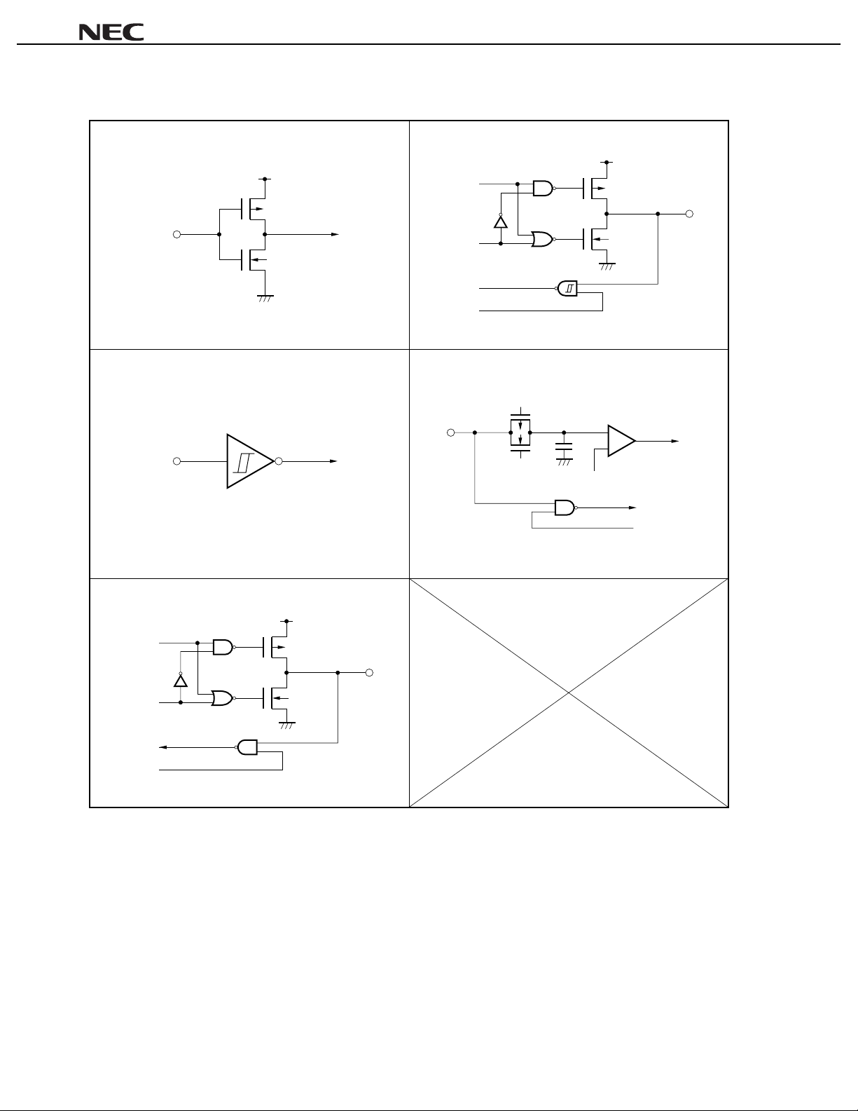
Figure 2-1. Pin Input/Output Circuits
µµµµ
PD70F3102-33
Type 1
Type 2
Type 5-K
V
DD
V
DD
P-ch
IN
N-ch
IN
Data
Output
disable
Input
enable
Type 9
P-ch
IN +
N-ch
V
P-ch
N-ch
Comparator
–
REF
(threshold voltage)
Input enable
IN/OUT
Schmitt-triggered input with hysteresis characteristics
Type 5
V
DD
Data
Output
disable
Input
enable
P-ch
IN/OUT
N-ch
Caution Replace VDD in the circuit diagrams with HVDD.
16
Preliminary Data Sheet U13844EJ2V0DS00
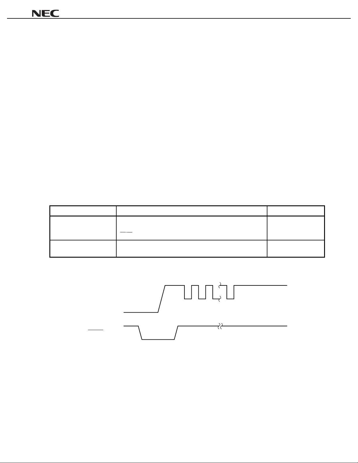
µµµµ
PD70F3102-33
3. FLASH MEMORY PROGRAMMING
The following two flash memory programming methods are available.
(1) On-board programming
The program is written to the flash memory using a dedicated flash programmer after the µPD70F3102-33 is
mounted on the target board. Install the connectors, etc., required for communication with the dedicated flash
programmer, on the target board.
(2) Off-board programming
The program is written to the flash memory using a dedicated adapter before the µPD70F3102-33 is mounted on
the target board.
3.1 Selection of Communication System
Writing to the flash memory is done via serial communication using the dedicated flash programmer. Select one
of the communication modes listed in Table 3-1. Base your selection of the communication mode on the selection
format shown in Table 3-1. Refer to the number of VPP pulses shown in Table 3-1 when selecting the communication
mode.
Table 3-1. Communication Modes
Communication Mode Pins Used Number of VPP Pulses
CSI0 SO0 (serial data output)
SI0 (serial data input)
SCK0 (serial clock i nput )
UART0 TXD0 (serial data output)
RXD0 (serial data input)
0
8
Figure 3-1. Communication Mode Selection Format
7.8 V
V
RESET
PP
DD
V
V
SS
V
DD
V
SS
Preliminary Data Sheet U13844EJ2V0DS00
17
µµµµ
PD70F3102-33
3.2 Flash Memory Programming Functions
Flash memory programming is performed by sending and receiving commands and data according to the selected
communication mode. Table 3-2 shows the main flash memory programming functions.
Table 3-2. Main Flash Memory Programming Functions
Function Description
Batch erasure Erases the contents of the entire memory.
Batch blank check Checks whether the entire memory has been erased.
Data write Writes data to flash mem ory based on the write start address and the number of bytes to be writ ten.
Batch verify Compares the contents of the entire m em ory with the input data.
3.3 Connecting the Dedicated Flash Programmer
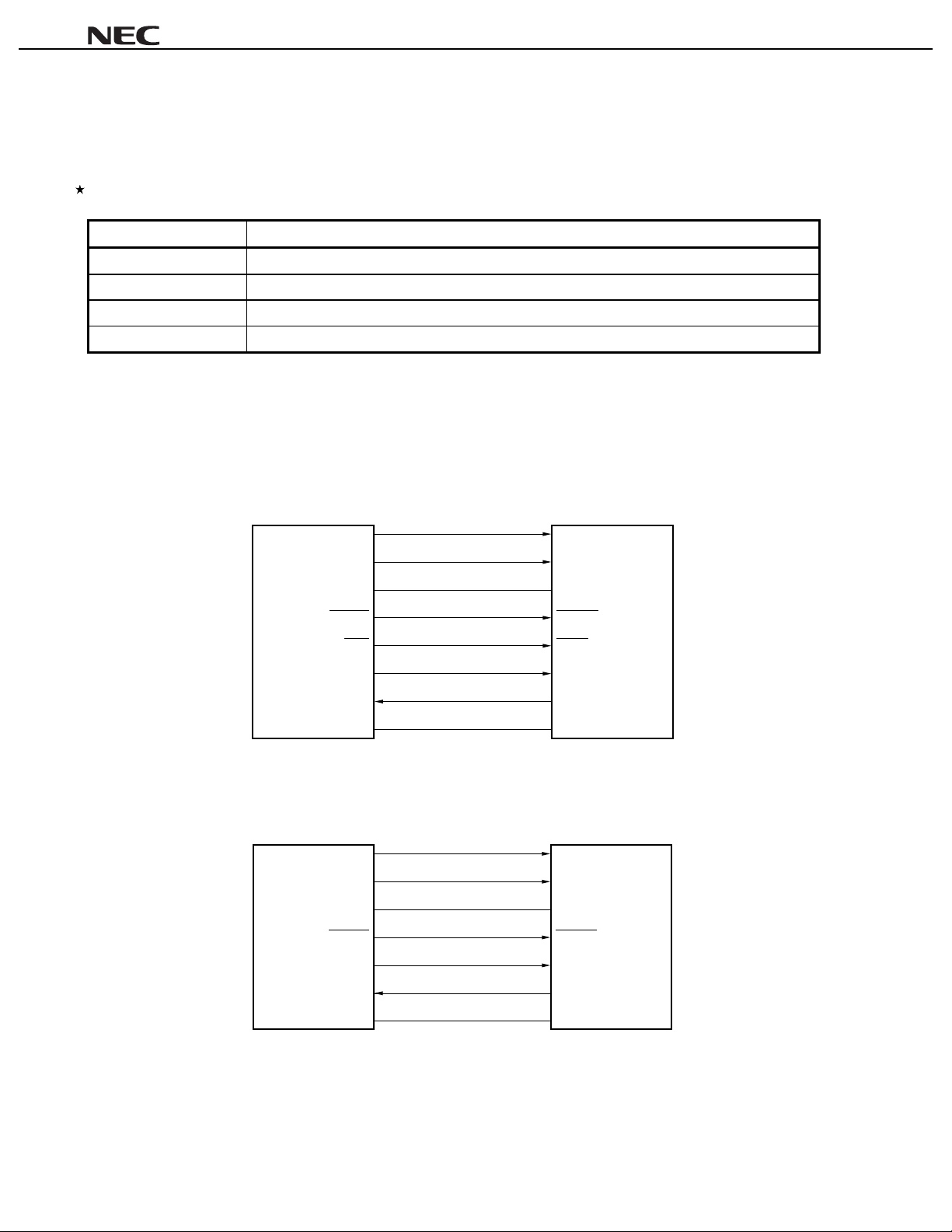
The connection of the dedicated flash programmer to the µPD70F3102-33 differs depending on the
communication mode. Figures 3-2 and 3-3 show the various connection types.
Figure 3-2. Connection of Dedicated Flash Programmer for CSI0 Mode
Dedicated flash programmer PD70F3102-33
CLK
PP
V
V
DD
RESET
SCK
SO
SI
V
SS
µ
CLK
PP
V
V
DD
RESET
SCK0
SI0
SO0
V
SS
Figure 3-3. Connection of Dedicated Flash Programmer for UART0 Mode
Dedicated flash programmer PD70F3102-33
CLK
V
PP
V
DD
RESET
TxD
µ
CLK
V
PP
V
DD
RESET
RXD0
18
RxD
SS
V
Preliminary Data Sheet U13844EJ2V0DS00
TXD0
SS
V
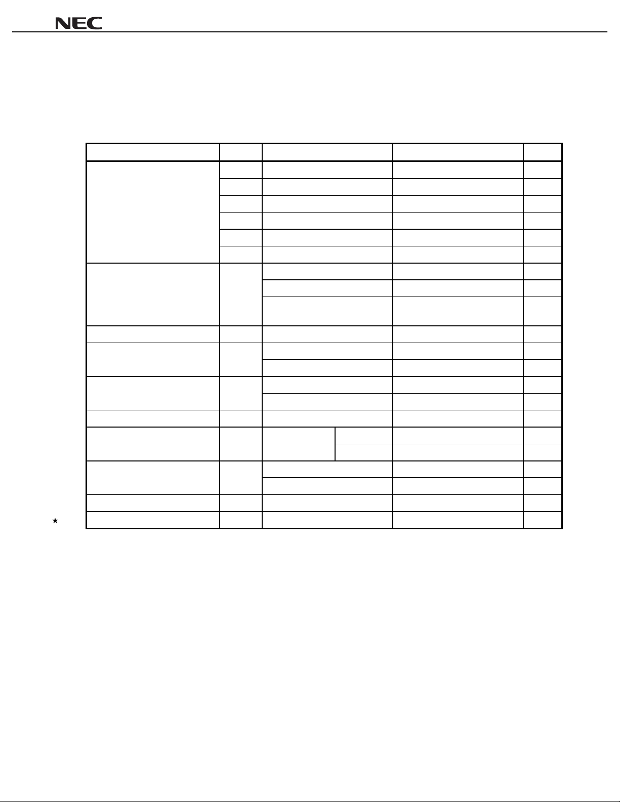
4. ELECTRICAL SPECIFICATIONS
4.1 Normal Operation Mode
Absolute Maximum Ratings (TA = 25°C)
Parameter Symbol Conditions Ratings Unit
DD
HV
CV
CV
AV
AV
AV
V
DD
DD
SS
DD
SS
I
K
OL
OH
O
IAN
REF
A
stg
Supply voltage
Input voltage V
Clock input voltage V
Output voltage V
voltage
Operating ambient temperature T
Storage temperature T
µµµµ
PD70F3102-33
VDD pin –0.5 to +4.6 V
HVDD pin, HVDD ≥ V
DD
–0.5 to +7.0 V
CVDD pin –0.5 to +4.6 V
CVSS pin –0.5 to +0.5 V
AVDD pin –0.5 t o HVDD + 0.5 V
AVSS pin –0.5 to +0.5 V
Except X1 pin, MODE 3/ VPP pin –0.5 to HVDD + 0.5 V
MODE3/VPP pin –0.5 to VDD + 0.5 V
MODE3/VPP pin in flash memory
–0.5 to +11.0 V
programming mode
X1, VDD = 3.0 to 3.6 V –0.5 to VDD + 1.0 V
1 pin 4.0 mAOutput current, low I
Total of all pins 100 mA
1 pin –4.0 mAOutput current, high I
Total of all pins –100 mA
HVDD = 5.0 V ±10% –0.5 to HVDD + 0.5 V
DD
≥ AV
DD
DD
–0.5 to HVDD + 0.5 VAnalog input voltage V
–0.5 to AVDD + 0.5 V
–0.5 to HVDD + 0.5 VA/D converter reference input
–0.5 to AVDD + 0.5 V
P70/ANI0 to
P77/ANI7 pins
AVDD > HV
HVDD ≥ AV
DD
DD
AVDD > HV
HV
–40 to +85 °C
–65 to +125 °C
Cautions 1. Do not directly connect output pins (or I/O pins) of IC products, and do not connect them
directly to VDD, VCC, or GND. However, open-drain pins and open-collector pins can be
directly connected to each other. Moreover, external circuits that implement a timing that
avoids conflict with the output of pins that go into high-impedance can be directly
connected.
2. Product quality may suffer if the absolute maximum rating is exceeded even momentarily
for any parameter. That is, the absolute maximum ratings are rated values at which the
product is on the verge of suffering physical damage, and therefore the product must be
used under conditions that ensure that the absolute maximum ratings are not exceeded.
The ratings and conditions indicated for DC characteristics and AC characteristics
represent the quality assurance range during normal operation.
Preliminary Data Sheet U13844EJ2V0DS00
19
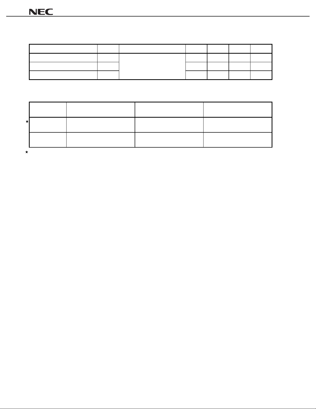
Capacitance (TA = 25°C, VDD = HVDD = CVDD = VSS = 0 V)
Parameter Symbol Conditions MIN. TYP. MAX. Unit
µµµµ
PD70F3102-33
Input capacitance C
I/O capacitance C
Output capacitance C
I
fC = 1 MHz
Unmeasured pins returned to 0 V
IO
O
15 pF
15 pF
15 pF
Operating Conditions
Operation
Mode
Direct mode 10 to 33 MHz –40 to +85°C VDD = 3.0 to 3.6 V,
PLL mode
Set the input clock frequency used in PLL mode to 4.0 to 6.6 MHz.
Note
Internal Operation Clock Frequency
(
)
φ
20 to 33 MHz
Note
Operating Ambient Temperature
(TA)
–40 to +85°C VDD = 3.0 to 3.6 V,
Supply Voltage (V
DD
HV
= 5.0 V ±10%
DD
HV
= 5.0 V ±10%
DD
, HVDD)
20
Preliminary Data Sheet U13844EJ2V0DS00
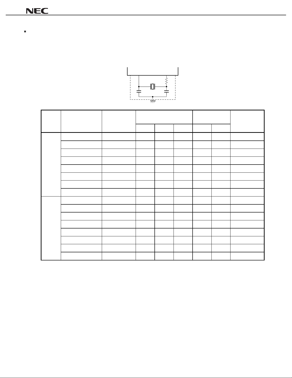
Recommended Oscillator
(a) Connection of ceramic resonator (TA = –40 to +85°C)
(i) Murata Mfg. Co., Ltd. (TA = –40 to +85°C)
µµµµ
PD70F3102-33
Type Product Name Oscillation
Frequency
XX
f
(MHz)
Surface
mount
Lead
CSAC4.00MGC040 4.0 100 100 0 3. 0 3.6 0.5
CSTCC4.00MG0H6 4.0 On-chip On-chip 0 3.0 3.6 0.3
CSAC5.00MGC040 5.0 100 100 0 3. 0 3.6 0.4
CSTCC5.00MG0H6 5.0 On-chip On-chip 0 3.0 3.6 0.2
CSAC6.60MT 6.6 30 30 0 3.0 3. 6 0.2
CSTCC6.60MG0H6 6.6 On-chip On-chip 0 3.0 3.6 0.1
CSAC8.00MT 8.0 30 30 0 3.0 3. 6 0.2
CSTCC8.00MG0H6 8.0 On-chip On-chip 0 3.0 3.6 0.3
CSA4.00MG040 4.0 100 100 0 3.0 3.6 0.5
CST4.00MGW040 4.0 On-chip On-chip 0 3.0 3.6 0.5
CSA5.00MG040 5.0 100 100 0 3.0 3.6 0.5
CST5.00MGW040 5.0 On-chip On-chip 0 3.0 3.6 0.5
CSA6.60MTZ 6.6 30 30 0 3.0 3.6 0.1
CST6.60MTW 6.6 On-chip On-chip 0 3.0 3.6 0.1
CSA8.00MTZ 8.0 30 30 0 3.0 3.6 0.1
CST8.00MTW 8.0 On-chip On-chip 0 3.0 3.6 0.1
X1
C1
Recommended Circuit
C1 (pF) C2 (pF) R
X2
R
C2
Constant
d
Oscillation Voltage
d
(kΩ) MIN. (V) MAX. (V)
Range
Oscillation
Stabilization Time
(MAX.)
OST
T
(ms)
Cautions 1. Connect the oscillator as closely to the X1 and X2 pins as possible.
2. Do not wire any other signal lines in the area indicated by the broken lines.
3. Thoroughly evaluate the matching between the
Preliminary Data Sheet U13844EJ2V0DS00
PD70F3102-33 and the resonator.
µµµµ
21
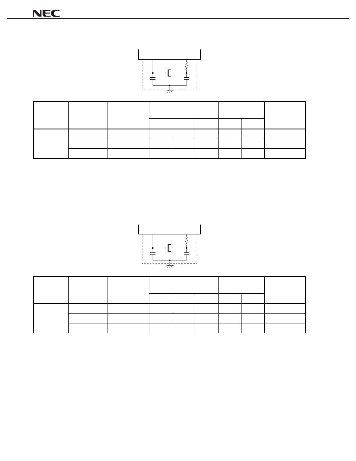
(ii) TDK Corporation (TA = –40 to +85°C)
µµµµ
PD70F3102-33
Manufacturer Product Name Oscillation
Frequency
XX
f
(MHz)
TDK
CCR4.0MC3 4.0 On-chip On-chip 0 3.0 3. 6 0.17
CCR5.0MC3 5.0 On-chip On-chip 0 3.0 3. 6 0.15
CCR8.0MC5 8.0 On-chip On-chip 0 3.0 3. 6 0.11
X1
C1
Recommended Circuit
C1 (pF) C2 (pF) R
X2
Constant
R
d
C2
Oscillation Voltage
d
(kΩ) MIN. (V) MAX. (V)
Cautions 1. Connect the oscillator as closely to the X1 and X2 pins as possible.
2. Do not wire any other signal lines in the area indicated by the broken lines.
3. Thoroughly evaluate the matching between the
PD70F3102-33 and the resonator.
µµµµ
(iii) Kyocera Corporation (TA = –20 to +80°C)
Range
Oscillation
Stabilization Time
(MAX.)
OST
T
(ms)
Manufacturer Product Name Oscillation
Frequency
XX
f
(MHz)
Kyocera
PBRC5.00BR-A 5.0 On-chip On-chip 0 3.0 3.6 0.06
PBRC6.00BR-A 6.0 On-chip On-chip 0 3.0 3.6 0.06
PBRC6.60BR-A 6.6 On-chip On-chip 0 3.0 3.6 0.06
X1
C1
Recommended Circuit
C1 (pF) C2 (pF) R
X2
Constant
R
d
C2
Oscillation Voltage
d
(kΩ) MIN. (V) MAX. (V)
Cautions 1. Connect the oscillator as closely to the X1 and X2 pins as possible.
2. Do not wire any other signal lines in the area indicated by the broken lines.
3. Thoroughly evaluate the matching between the
PD70F3102-33 and the resonator.
µµµµ
Range
Oscillation
Stabilization Time
(MAX.)
OST
T
(ms)
22
Preliminary Data Sheet U13844EJ2V0DS00

(b) External clock input (TA = –40 to +85°C)
X1 X2
External clock
Caution Input a CMOS level voltage to the X1 pin.
Cautions when turning on/off the power
PD70F3102-33 is configured with power supply pins for the internal unit (VDD) and for the external pins
The
µ
(HVDD).
The operation guaranteed range is VDD = CV
ports may be undefined when the voltage exceeds this range.
DD
= 3.0 to 3.6 V, HVDD = 5.0 V ±10%. The input and output state of
Open
µµµµ
PD70F3102-33
Preliminary Data Sheet U13844EJ2V0DS00
23
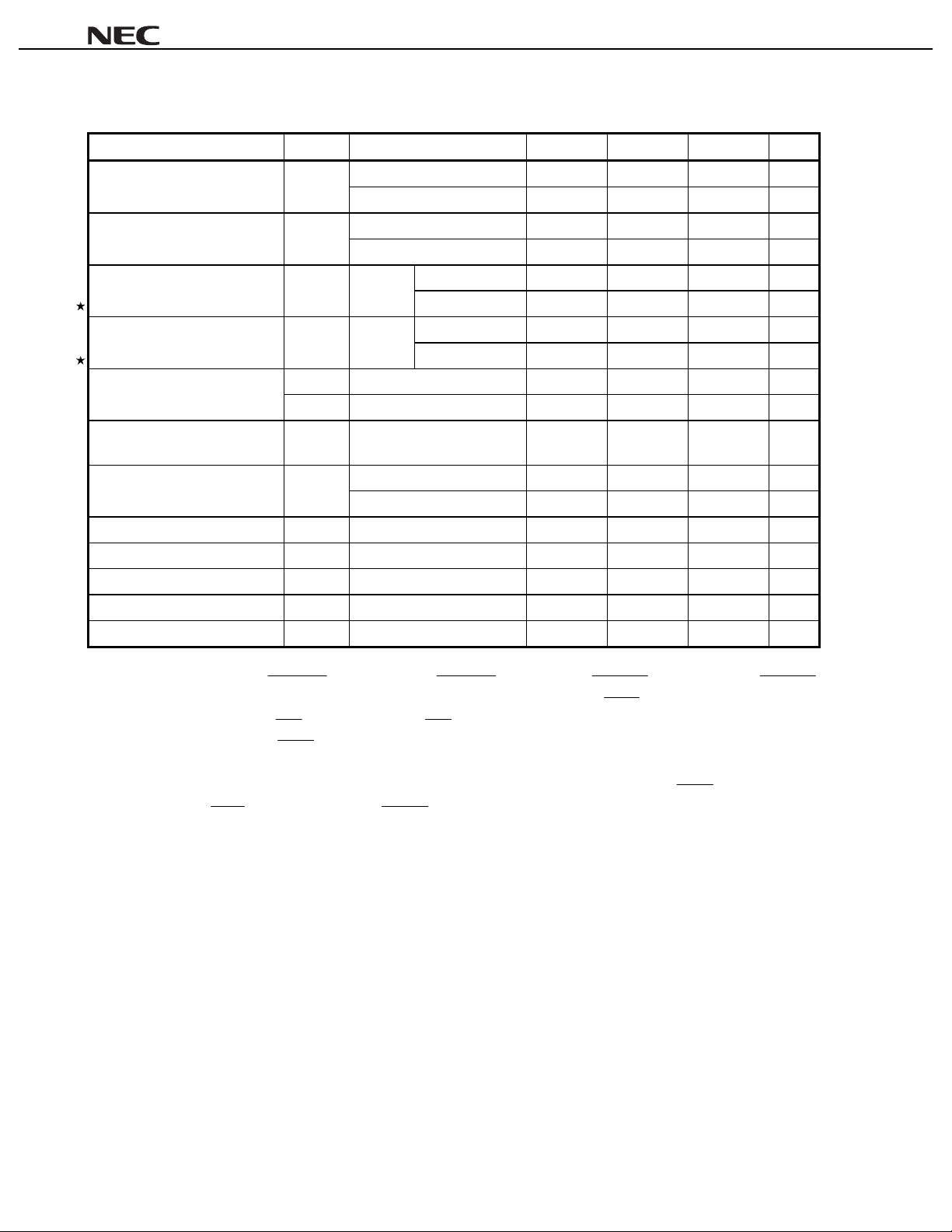
µµµµ
PD70F3102-33
DC Characteristics (TA = –40 to 85°C, VDD = CVDD = 3.0 to 3.6 V, HVDD = 5.0 V
Parameter Symbol Conditions MIN. TYP. MAX. Unit
Except
Note 1
Except
Note 1
X1 pin
X1 pin
Note 1
and
Notes 1
2
Direct mode 0.8V
PLL mode 0.8V
Direct mode –0.3 0.15V
2.2 HV
DD
0.8HV
–0.5 +0.8 V
–0.5 0.2HV
DD
DD
PLL mode –0.3 0.15V
, rising edge
Note 1
, falling edge
Note 1
Note 1
IOH = –2.5 mA 0.7HV
IOH = –100 µAHV
0.5 V
DD
DD
– 0.4 V
IOL = 2.5 mA 0.45 V
VI = HVDD, except
VI = 0 V, except
DD
VO = HV
Note 2
Note 2
VO = 0 V –10
Input voltage, low V
Schmitt-triggered input
threshold voltage
Schmitt-triggered input
hysteresis widt h
HV
HV
HV
–HV
Output voltage, low, V
Input leakage current, high I
Input leakage current, low I
Output leakage current, high I
Output leakage current, low I
LIH
LOH
LOL
IH
IL
XH
XL
+
T
–
T
+
T
–
T
OH
OL
LIL
10%, VSS = 0 V)
±±±±
3.0 V
2.0 V
DD
+ 0.3 VInput voltage, high V
HVDD + 0.3 V
DD
VDD + 0.3 VClock input voltage, high V
VDD + 0.3 V
DD
DD
10
–10
10
V
VClock input voltage, low V
V
VOutput voltage, high V
A
µ
A
µ
A
µ
A
µ
Notes 1.
2.
Remark
P04/INTP100/DMARQ0 to P07/INTP103/DMARQ3, P14/INTP110/DMAAK0 to P17/INTP113/DMAAK3,
P34/INTP130, P35/INTP131/SO2, P36/INTP132/SI2, P37/INTP133/SCK2,
P104/INTP120/TC0 to P107/INTP123/TC3, P114/INTP140, P115/INTP141/SO3, P116/INTP142/SI3,
P117/INTP143/SCK3, P124/INTP150 to P126/INTP152, P127/INTP153/ADTRG, P02/TCLR10,
P12/TCLR11, P32/TCLR13, P102/TCLR12, P112/TCLR14, P122/TCLR15, P03/TI10, P13/TI11,
P33/TI13, P103/TI12, P113/TI14, P123/TI15, P20/NMI, P23/RXD0/SI0, P24/SCK0, P26/RXD1/SI1,
P27/SCK1, MODE0 to MODE2, RESET
When using the P70/AN10 to P77/ANI7 pins as analog inputs.
A
TYP. values are reference values for when T
= 25°C, VDD = CVDD = 3.3 V, HVDD = 5.0 V.
24
Preliminary Data Sheet U13844EJ2V0DS00
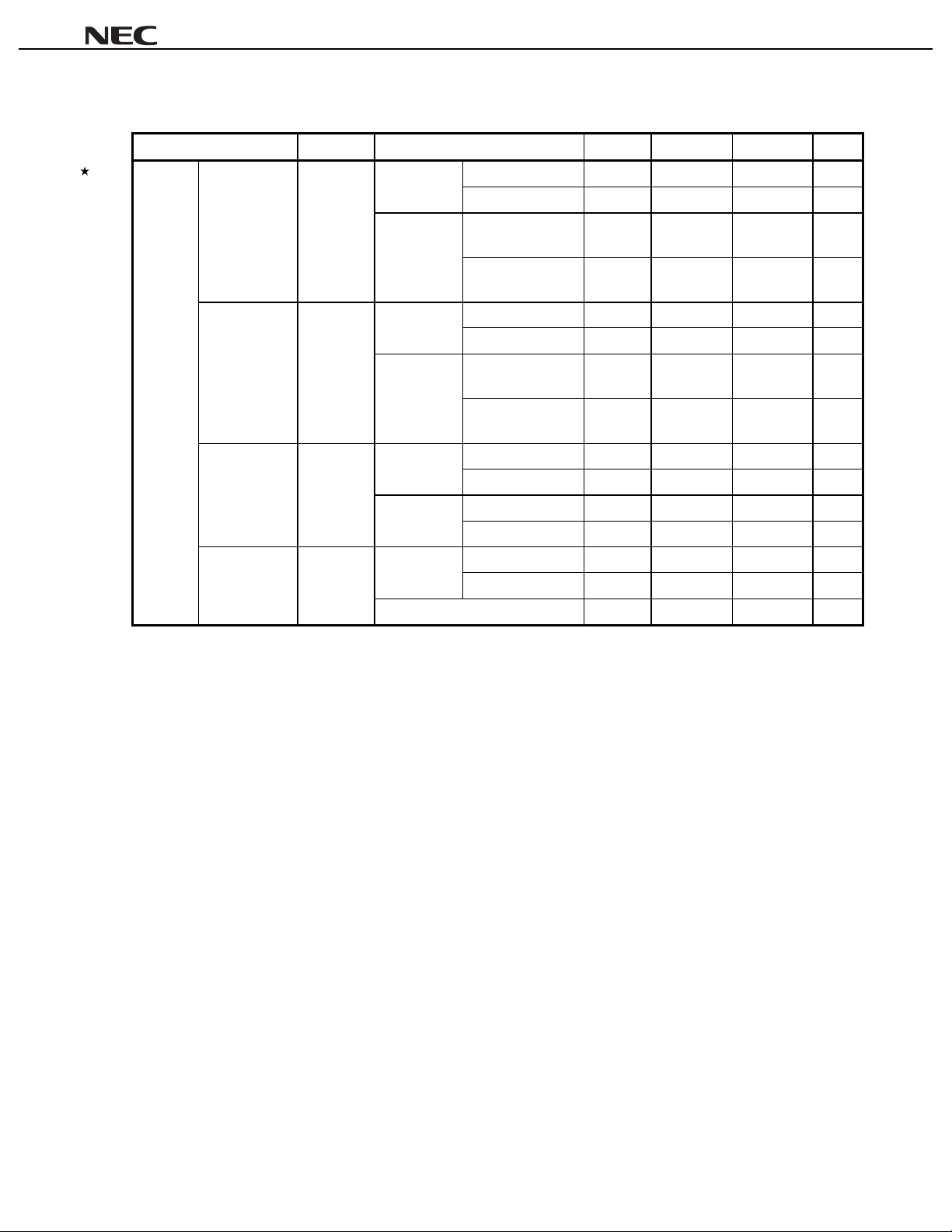
µµµµ
PD70F3102-33
DC Characteristics (TA = –40 to 85°C, VDD = CVDD = 3.0 to 3.6 V, HVDD = 5.0 V
Parameter Symbol Conditions MIN. TYP. MAX. Unit
DD
DD
DD
DD
DD
DD
40°C < T
DD
DD
DD
DD
DD
DD
A
≤ +85°C
Supply
current
During normal I
During HALT I
During IDLE I
During STOP I
DD1
DD2
DD3
DD4
PLL mode
PLL mode
PLL mode
DD
HV
VDD + CV
HV
VDD + CV
HV
VDD + CV
HV
VDD + CV
HV
VDD + CV
HV
VDD + CV
HV
DD
–40°C ≤ TA ≤ +40°C
+
10%, VSS = 0 V)
±±±±
X
2.0 × f
X
1.8 × f
X
2.7 × f
– 17.0
X
1.3 × f
– 3.6
X
1.4 × f
X
0.8 × f
X
1.8 × f
– 10.0
X
0.8 × f
– 1.0
3.0 10 mADirect mode
0.5 1.0 mA
3.0 10 mA
0.5 1.0 mA
20 50
20 600
10 20
4.5 × f
3.0 × f
4.5 × f
3.0 × f
3.0 × f
1.5 × f
3.0 × f
1.5 × f
X
mADirect mode
X
mA
X
mA
X
mA
X
mADirect mode
X
mA
X
mA
X
mA
AVDD + CV
µ
A
µ
A
µ
Remarks 1.
TYP. values are reference values for when T
Direct mode: fX = 10 to 33 MHz
2.
PLL mode: fX = 20 to 33 MHz
The fX unit is MHz.
3.
A
= 25°C, VDD = CVDD = 3.3 V, HVDD = 5.0 V.
Preliminary Data Sheet U13844EJ2V0DS00
25
 Loading...