NEC uPD63335GA-9EU Datasheet

DATA SHEET
MOS INTEGRATED CIRCUITS
PD63335
µµµµ
STEREO SOUND CODEC
DESCRIPTION
The
PD63335 is a stereo sound codec LSI that enables full-duplex communications and features two channels
µ
each of on-chip 16-bit ADC and DAC circuits for mutual conversion between digital signals and audio analog signals
(having a maximum signal bandwidth of 20 kHz).
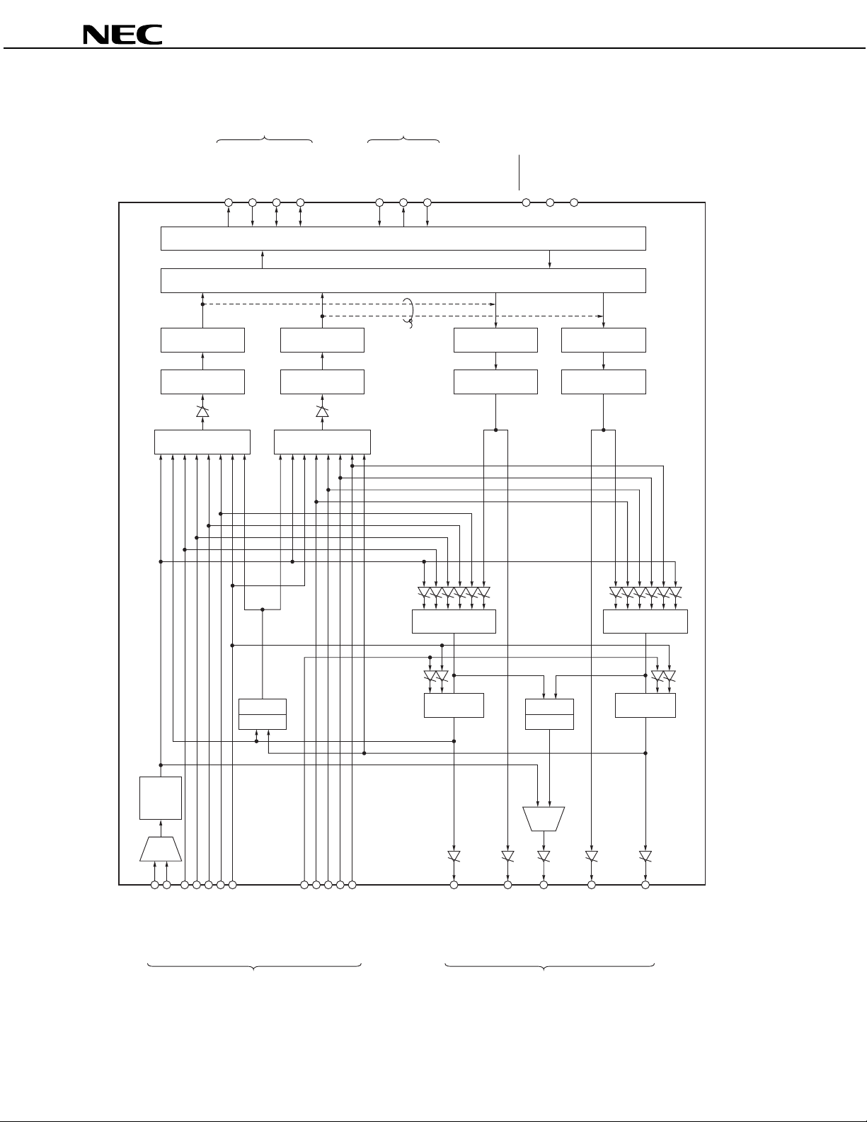
The analog signal input block enables four pairs of stereo signals plus three monaural signals to be output from
the output stage's internal mixing circuit, which can then be multiplexed and input to the ADC. One type of monaural
signal can be selected from two external pins via a selector as a monaural signal connected to an internal
microphone amplifier (MIC amp), with selectable gain of 0 dB or 20 dB.
The analog signal output block enables mixed output of analog signals output by the DAC, four pairs of stereo
analog signals, and an output signal from the MIC amp, and the volume of each signal can be controlled
independently before mixing. The digital audio signal I/O block supports an audio-type serial interface (two's
complement). In addition, a clocked serial interface (CSI) can be used for direct connection to a general-purpose
microcontroller for access to internal registers such as for volume control.
FEATURES
• Two channels each of over sample
• ADC SNR = 85 dB Typ.
• DAC SNR = 90 dB Typ.
• ADC and DAC digital filter characteristics
• Pass band ripple: ±0.1 dB (0 to 0.4 f
• Stop band attenuation: −74 dB (0.6 f
• Sampling frequency (f
• Division rate from master clock can be set to 3072, 1536, 768, or 512
• Analog input block includes a multiplexer and analog output block includes a mixing circuit
• Low-noise monaural MIC amp is on chip
• On-chip reference voltage power supply (1.4 V (TYP.))
• Low supply voltage operation: DV
• Support for power down mode in each internal block
• Operating ambient temperature: −40 to +85°C
): 0.4 to 48 kHz
S
∆
Σ type ADC and DAC
) for ADC and DAC
S
) or above for ADC and DAC
S
= 3.3 V, AVDD = 3.3 V
DD
APPLICATIONS
• Speech recognition systems, including car navigation systems
• Electronic toys with speech/audio I/O functions
ORDERING INFORMATION
Part Number Package
PD63335GA-9EU
µ
48-pin plastic TQFP (fine pitch) (7 × 7)
The information in this document is subject to change without notice. Before using this document, please
confirm that this is the latest version.
Not all devices/types available in every country. Please check with local NEC representative for
availability and additional information.
Document No. S15003EJ6V0DS00 (6th edition)
Date Published February 2002 N CP(K)
Printed in Japan
The mark shows major revised points.
2000©
µ
PD63335
BLOCK DIAGRAM
Digital data interface Digital command interface
SO
SI
LRCLK
BIT_CLK
MSWDT
MSRDT
MSCLK
I/O Interface
Digital Filter
RESET
XTL_IN
XTL_OUT
MIC
Stereo Mix/L
IN1L
IN2L
IN3L
IN4L
IN5
Mono Mix
Mono Mix
Mixer
−6 dB
DecimatorDecimator
MultiplexerMultiplexer
MIC
Mono Mix
IN5
ADCADC
IN1R
IN2R
IN3R
IN4R
Stereo Mix/R
IN5
IN6
Stereo Mix/L
Stereo Mix/R
Loop-back
(test mode)
IN4L
IN3L
IN2L
IN1L
MIC
MIC
InterpolatorInterpolator
DACDAC
IN4R
IN3R
IN2R
IN1R
Mixer Mixer
Mixer Mixer
−6 dB
Mixer
MC20
0 dB/
20 dB
MS
MIC2
MIC1
IN1L
IN2L
IN3L
IN4L
IN5
IN6
IN1R
Remark The MS and MIX blocks are selectors.
2
IN3R
IN4R
IN2R
OUTL
Data Sheet S15003EJ6V0DS
DAC MONO
MIX
DACL
DACR
OUTR
MONO_OUT
Analog output pinsAnalog input pins
µ
PD63335
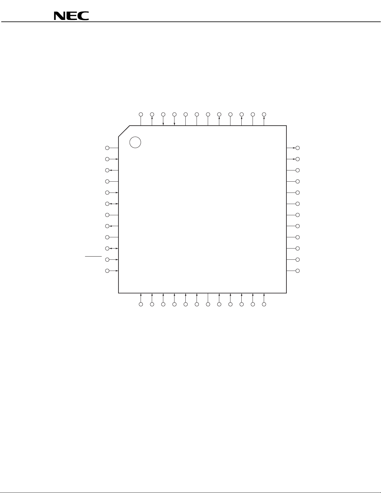
PIN CONFIGURATION (TOP VIEW)
48-pin plastic TQFP (fine pitch) (7 × 7)
•µPD63335GA-9EU
DV
DD1
XTL_IN
XTL_OUT
DV
SS1
BIT_CLK
SS2
DV
SO
DV
DD2
LRCLK
RESET
IN6
DD3
DV
MSRDT
MSWDT
TEST2
MSCLK
TEST1
SS2
AV
DD2
DACR
NC
AV
DACL
MONO_OUT
48 47 46 45 44 43 42 41 40 39 38 37
1
2
3
4
SI
5
6
7
8
9
10
11
12
36
35
34
33
32
31
30
29
28
27
26
25
OUTR
OUTL
NC
NC
NC
NC
AFILT2
AFILT1
NC
Vref
AV
SS1
AV
DD1
13 14 15 16 17 18 19 20 21 22 23 24
IN5
IN3L
IN3R
IN2L
IN2R
IN1L
IN1R
MIC1
MIC2
IN4L
IN1_GND
Data Sheet S15003EJ6V0DS
IN4R
3

µ
PD63335
PIN FUNCTIONS
Pin No. Symbol I/O Function
(1/2)
1DV
2 XTL_IN I
DD1
− Digital power supply
Crystal resonator connection pin/external master clock input (see 1.3 Clock)
3 XTL_OUT O Crystal resonator connection pin. Leave this pin open when using an external master
clock.
4DV
5SI I
6 BIT_CLK I/O
7DV
SS1
SS2
− Digital ground
Data input for serial data interface
Bit sync clock for serial data interface
− Digital ground
Note
Note
8 SO O Data output for serial data interface
9DV
10 LRCLK I/O
DD2
− Digital power supply
Frame sync clock for serial data interface
Note
_______
11
RESET
I Reset signal input. Sets reset mode when low.
12 IN6 I Analog audio monaural input 6
13 IN5 I Analog audio monaural input 5
14 IN3L I Analog audio input 3, L channel
15 IN3R I Analog audio input 3, R channel
16 IN2L I Analog audio input 2, L channel
17 IN2R I Analog audio input 2, R channel
18 IN1L I Analog audio input 1, L channel
19 IN1_GND − AC ground pin for IN1. Generally connect to AVSS via a 1 µF capacitor.
20 IN1R I Analog audio input 1, R channel
21 MIC1 I MIC input 1
22 MIC2 I MIC input 2
23 IN4L I Analog audio input 4, L channel
24 IN4R I Analog audio input 4, R channel
25 AV
26 AV
DD1
SS1
− Analog power supply
− Analog ground
27 Vref − Reference voltage output for connecting bypass capacitor
28 NC − Not used. Leave this pin open.
29 AFILT1 − ADC L channel anti alias filter pin
30 AFILT2 − ADC R channel anti alias filter pin
31 NC − Not used. Leave this pin open.
32 NC − Not used. Leave this pin open.
33 NC − Not used. Leave this pin open.
34 NC − Not used. Leave this pin open.
Note The SI, BIT_CLK, and LRCLK pins are neither pulled up nor pulled down within the LSI. Since malfunction
may occur if these pins are somehow set to high impedance, pull-up or pull-down should be performed
externally, via a resistor.
4
Data Sheet S15003EJ6V0DS
µ
PD63335
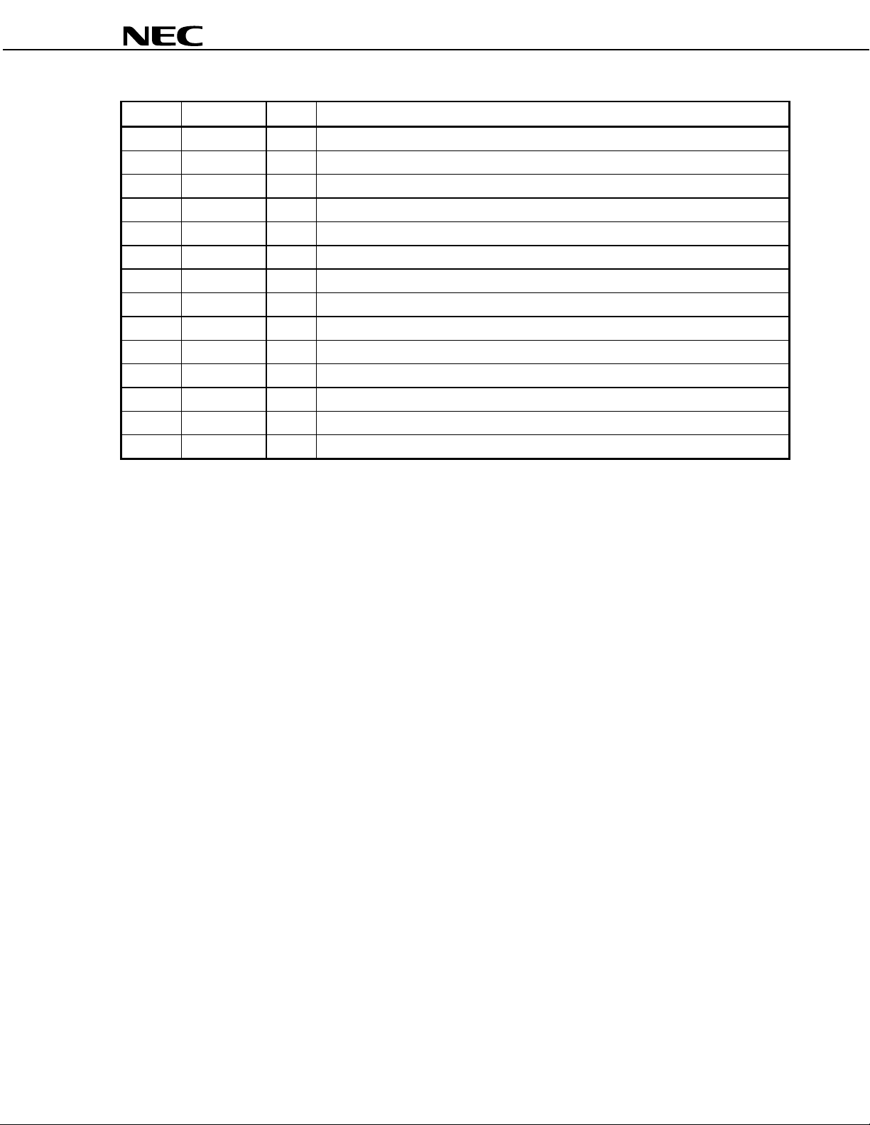
Pin No. Symbol I/O Function
35 OUTL O Analog audio output pin, L channel
36 OUTR O Analog audio output pin, R channel
37 MONO_OUT O Analog audio monaural output
38 AV
39 DACL O Analog DAC signal output, L channel
40 NC − Not used. Leave this pin open.
41 DACR O Analog DAC signal output, R channel
42 AV
43 TEST1 − Test pin for IC sorting. Leave this pin open.
44 TEST2 − Test pin for IC sorting. Leave this pin open.
45 MSCLK I Sync clock input for serial command interface
46 MSWDT I Input for serial command interface
47 MSRDT O Output for serial command interface
48 DV
DD2
SS2
DD3
− Analog power supply
− Analog ground
− Digital power supply
(2/2)
Data Sheet S15003EJ6V0DS
5

µ
PD63335
CONTENTS
1. DESCRIPTION OF FUNCTIONS ........................................................................................................................... 8
1.1 Analog Input Block ........................................................................................................................................ 8
1.2 Analog Output Block ..................................................................................................................................... 8
1.3 Clock ............................................................................................................................................................... 8
1.3.1 Switching external master clock frequency ..................................................................................9
1.4 Reset ............................................................................................................................................................. 10
1.5 Pin to Connect Noise-Reducing Capacitor................................................................................................ 10
1.6 Digital Interfaces .......................................................................................................................................... 11
1.6.1 Serial command interface ............................................................................................................. 11
1.6.2 Serial data interface....................................................................................................................... 12
1.6.3 Data format of FSDF2:FSDF1:FSDF0:LRCLKS = 0:0:0:0 ............................................................ 16
1.6.4 Data format of FSDF2:FSDF1:FSDF0:LRCLKS = 0:0:0:1 ............................................................ 16
1.6.5 Data format of FSDF2:FSDF1:FSDF0:LRCLKS = 0:0:1:0 ............................................................ 17
1.6.6 Data format of FSDF2:FSDF1:FSDF0:LRCLKS = 0:0:1:1 ............................................................ 17
1.6.7 Data format of FSDF2:FSDF1:FSDF0:LRCLKS = 0:1:0:0 ............................................................ 18
1.6.8 Data format of FSDF2:FSDF1:FSDF0:LRCLKS = 0:1:0:1 ............................................................ 18
1.6.9 Data format of FSDF2:FSDF1:FSDF0:LRCLKS = 0:1:1:0 ............................................................ 19
1.6.10 Data format of FSDF2:FSDF1:FSDF0:LRCLKS = 0:1:1:1 ............................................................ 19
1.6.11 Data format of FSDF2:FSDF1:FSDF0:LRCLKS = 1:0:0:0 ............................................................ 20
1.6.12 Data format of FSDF2:FSDF1:FSDF0:LRCLKS = 1:0:0:1 ............................................................ 20
1.6.13 Data format of FSDF2:FSDF1:FSDF0:LRCLKS = 1:0:1:0 ............................................................ 21
1.6.14 Data format of FSDF2:FSDF1:FSDF0:LRCLKS = 1:0:1:1 ............................................................ 21
1.6.15 Data format of FSDF2:FSDF1:FSDF0:LRCLKS = 1:1:0:0 ............................................................ 22
1.6.16 Data format of FSDF2:FSDF1:FSDF0:LRCLKS = 1:1:0:1 ............................................................ 22
1.6.17 Data format of FSDF2:FSDF1:FSDF0:LRCLKS = 1:1:1:0 (initial value) ..................................... 23
1.6.18 Data format of FSDF2:FSDF1:FSDF0:LRCLKS = 1:1:1:1 ............................................................ 23
1.7 Usage Precautions ...................................................................................................................................... 23
2. REGISTERS........................................................................................................................................................... 24
2.1 Individual Registers..................................................................................................................................... 25
2.1.1 Serial command interface check bit (SICK)................................................................................. 25
2.1.2 Reset/clock status register (00h).................................................................................................. 25
2.1.3 Interface/timing register (01h) ...................................................................................................... 26
2.1.4 Input select register (02h) ............................................................................................................. 27
2.1.5 ADC input gain registers (03h, 04h) ............................................................................................. 28
2.1.6 IN1 volume registers (05h, 06h).................................................................................................... 29
2.1.7 IN2 volume registers (07h, 08h).................................................................................................... 30
2.1.8 IN3 volume registers (09h, 0Ah) ................................................................................................... 31
2.1.9 IN4 volume registers (0Bh, 0Ch)................................................................................................... 32
2.1.10 IN5 volume register (0Dh) ............................................................................................................. 33
2.1.11 MIC volume register (0Eh)............................................................................................................. 34
2.1.12 IN6 volume register (0Fh).............................................................................................................. 35
2.1.13 DAC volume registers (10h, 11h).................................................................................................. 36
2.1.14 OUT master volume registers (12h, 13h) ..................................................................................... 37
6
Data Sheet S15003EJ6V0DS

µ
PD63335
2.1.15 DAC master volume registers (14h, 15h)......................................................................................38
2.1.16 MONO output master volume register (16h) ................................................................................39
2.1.17 Path select register (17h) ...............................................................................................................40
2.1.18 Power down control register (18h)................................................................................................41
2.1.19 Warm reset register (7Fh) ..............................................................................................................43
3. ELECTRICAL SPECIFICATIONS..........................................................................................................................44
4. APPLICATION CIRCUIT EXAMPLE ....................................................................................................................51
5. RECOMMENDED LAND PATTERN.....................................................................................................................52
6. PACKAGE DRAWING...........................................................................................................................................53
7. RECOMMENDED SOLDERING CONDITIONS....................................................................................................54
Data Sheet S15003EJ6V0DS
7
µ
PD63335
1. DESCRIPTION OF FUNCTIONS
1.1 Analog Input Block
PD63335 features an on-chip two-channel ADC, which can convert analog signals selected by the
The
µ
multiplexer at the previous stage and input via the analog input pin to digital signals. An amplifier is configured
between the ADC and multiplexer, and the input gain can be set in a range from 0 dB to 22.5 dB.
The multiplexer receives signals that are input from the analog output block’s mixer circuit, and four-channel
stereo signals, two monaural signals, and a monaural MIC input signal (selected from two input pins) from the analog
input pins.
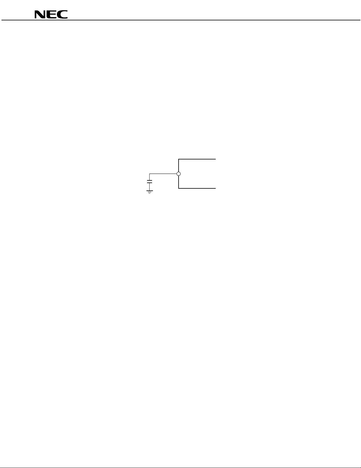
The IN1 input has a dedicated AC ground pin for canceling common-mode noise. Use of the IN1_GND pin
enables connections to output pins that have a ground line, such as a CD audio output pin, via a 4.7 µF capacitor. If
not using IN1_GND, connect to a ground via a 1
Figure 1-1. Connection Example When Not Using IN1_GND
1.2 Analog Output Block
The analog output block includes two stereo output amplifiers, a monaural output amplifier, and a mixer circuit.
The mixer circuit can be used to mix not only stereo analog signals from the DAC but also four pairs of stereo signals
(IN1 to IN4), one monaural signal, and one MIC input signal (selected from two input pins). The analog signals from
the DAC output can be connected to the mixer circuit or DAC L/R output via volume circuits. Monaural mixed signals
to the monaural output selector (MIX) are the sum of the L channel/R channel mixer circuit output to which –6 dB of
gain adjustment is applied within the LSI.
F capacitor (see Figure 1-1).
µ
PD63335
µ
1 F
µ
IN1_GND
1.3 Clock
PD63335 features an on-chip clock generator. The µPD63335’s master clock can be generated if a crystal
µ
The
resonator is connected via the XTL_IN or XTL_OUT pin.
The on-chip clock generator can be used only at the 24.576 MHz setting.
In addition, an external master clock can be input to the on-chip clock generator. In such cases, input the clock
signal directly to the XTL_IN pin and leave the XTL_OUT pin open. In this case, the recommended frequency range
of the external master clock is from 1.024 MHz to 24.576 MHz.
8
Data Sheet S15003EJ6V0DS

µ
PD63335
1.3.1 Switching external master clock frequency
To switch the external master clock frequency during ADC and DAC operation, use the following procedure.
(1) When using the Master mode (LRCLK, BIT_CLK generated internally)
<1> Set the DAC volume register (10h, 11h) and the DAC master volume register (14h, 15h) to MUTE
Note 1
<2> Switch the external master clock frequency.
<3> Set the LRCLK/BIT_CLK operation mode (if there is a change) (use the reset/clock status register (00h)).
<4> Set the audio format (if there is a change) (use the interface/timing register (01h)).
<5> Set the DAC volume register (10h, 11h) and DAC master volume register (14h, 15h)
Note 2
Notes 1. The instant that the external master clock frequency is switched, noise may occur. For this reason,
before switching the external master clock, set the volume for the DAC output to MUTE.
2. To prevent popping noises, after switching the external master clock frequency and following the
lapse of an interval of time sufficient for three or more LRCLK cycles to be supplied, cancel the
MUTE setting of the volume for the DAC output.
Also handle the ADC output data (SO) as valid data once the same interval of time has elapsed.
(2) When using the slave mode (LRCLK, BIT_CLK supplied from external)
<1> Set the DAC volume register (10h, 11h) and the DAC master volume register (14h, 15h) to MUTE
Note 1
<2> Power down the ADC and DAC (use the power down control register (18h)).
<3> Switch the external master clock, LRCLK, BIT_CLK frequency.
<4> Set the LRCLK/BIT_CLK operation mode (if there is a change) (use the reset/clock status register (00h)).
<5> Set the audio format (if there is a change) (use the interface/timing register (01h)).
<6> Cancel ADC, DAC power down (use the power down control register (18h)).
<7> Set the DAC volume register (10h, 11h) and DAC master volume register (14h, 15h)
Note 2
.
.
.
Notes 1. Immediately after the ADC and DAC are powered down, noise may occur in the ADC and DAC
outputs. For this reason, before powering down the ADC and DAC, set the volume for the DAC
output to MUTE.
2. To prevent popping noises, after canceling power down and following the lapse of an interval of time
sufficient for three or more LRCLK cycles to be supplied, cancel the MUTE setting of the volume for
the DAC output. Also handle the ADC output data (SO) as valid data once the same interval of time
has elapsed.
Data Sheet S15003EJ6V0DS
9
µ
PD63335
1.4 Reset
PD63335 features three reset modes.
The
µ
(1) Cold reset
Cold reset is controlled by input signals via the
_______
RESET pin, and is used to initialize the
PD63335. Registers
µ
are reset to their initial values.
(2) Warm reset
A warm reset is used to reset the digital command interface for any reason. When FFh is written to the warm
reset register (7Fh), the
PD63335 performs a warm reset. Register values are retained during a warm reset.
µ
(3) Register reset
This initializes the µPD63335’s internal registers. All registers are reset, except for the following registers.
• Reset/clock status register (00h)
• Interface/timing register (01h)
• Power down control register (18h)
1.5 Pin to Connect Noise-Reducing Capacitor
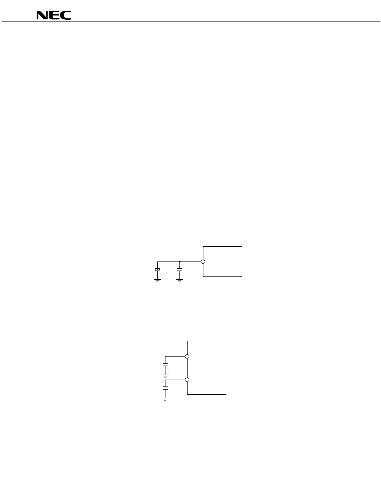
Pin 27 is a reference voltage pin that is used to connect to a bypass capacitor for stabilizing the internal reference
voltage. Connect the bypass capacitor as shown in the figure below.
Figure 1-2. Example of Bypass Capacitor Connection
µ
PD63335
Tantalum
capacitor
µ
4.7 F
+
0.1 F
Ceramic capacitor
Vref
µ
Pins 29 and 30 are used to connect capacitors for the ADC’s anti alias filter. Connect the capacitor as shown in
the figure below.
Figure 1-3. Example of Capacitor Connection for Anti Alias Filter
PD63335
µ
AFILT1
270 pF
AFILT2
270 pF
10
Data Sheet S15003EJ6V0DS
µ
PD63335
1.6 Digital Interfaces
PD63335 uses two different interfaces to connect to an external host processor (such as a CPU or sound
The
µ
controller). One is the serial command interface that controls the µPD63335, and the other is the serial data interface
that is used for data input and output.
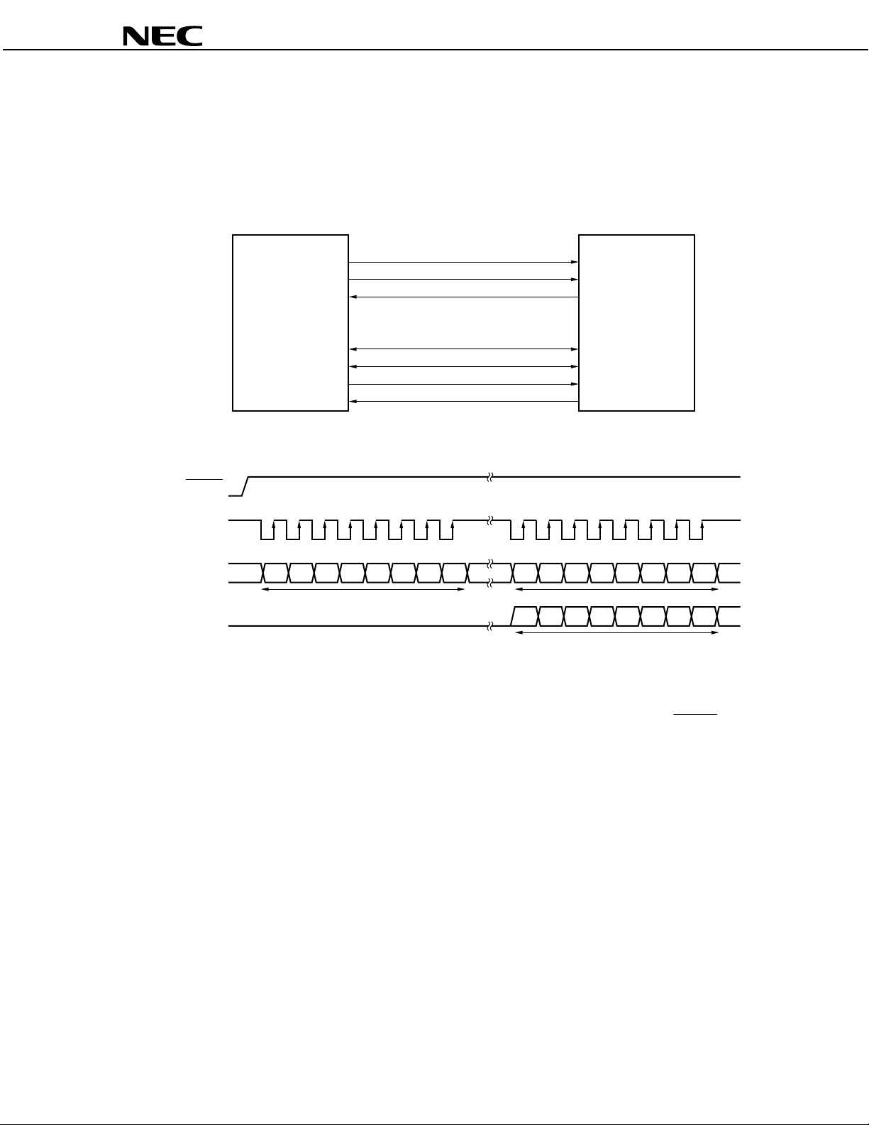
Figure 1-4. Digital Interfaces
Serial command interface
MSCLK
MSWDT
MSRDT
Host processor
Serial data interface
LRCLK
BIT_CLK
SI
SO
PD63335
µ
1.6.1 Serial command interface
RESET
MSCLK
MSWDT
(Input)
MSRDT
(Output)
When accessing the
Bit7 Bit6 Bit5 Bit4 Bit3 Bit2 Bit1 Bit0
Address Write data
PD63335 from an external host processor, use the clocked serial interface (MSCLK,
µ
Bit7 Bit6 Bit5 Bit4 Bit3 Bit2 Bit1 Bit0
Bit7 Bit6 Bit5 Bit4 Bit3 Bit2 Bit1 Bit0
Read data
MSWDT, MSRDT).
Transfer of addresses begins in sync with the rising edge of MSCLK, immediately after the RESET signal goes
from low level to high level. Addresses consist of eight bits, of which bit 7 indicates the read/write attribute for
access.
When a “1” is transferred to bit 7 in the address, a read operation is performed. After an address is input via the
MSWDT pin, the contents of the corresponding register are output via the MSRDT pin.
When a “0” is transferred to bit 7 in the address, a write operation is performed. Once the address is sent from the
host processor, 8-bit data is written.
The µPD63335 uses the data to check for bit drift in the serial command interface so as to ensure accurate control
from the host processor.
When communication is being performed correctly, the D6 address bit of all the registers except the warm reset
register (7Fh) is always “0”, and the D7 and D6 data bits are always “01”. The D6 data bit (SICK) is used to check for
the occurrence of bit displacement among the serial command interface bits. For details of the SICK bit, refer to
2.1.1 Serial command interface check bit (SICK).
Data Sheet S15003EJ6V0DS
11
µ
PD63335
1.6.2 Serial data interface
Four sampling frequency settings can be made for the
PD63335 by setting the RATE[1:0] bit in an internal
µ
register (00h). Registers 00h and 01h can be used to set the polarity of the frame signal (LRCLK) and to switch the
I/O status of the LRCLK and BIT_CLK signals. Some noise may occur when switching the format of the serial data
interface during operation. Before switching, set the analog output volume to “mute” (see 2.1.14 to 2.1.16).
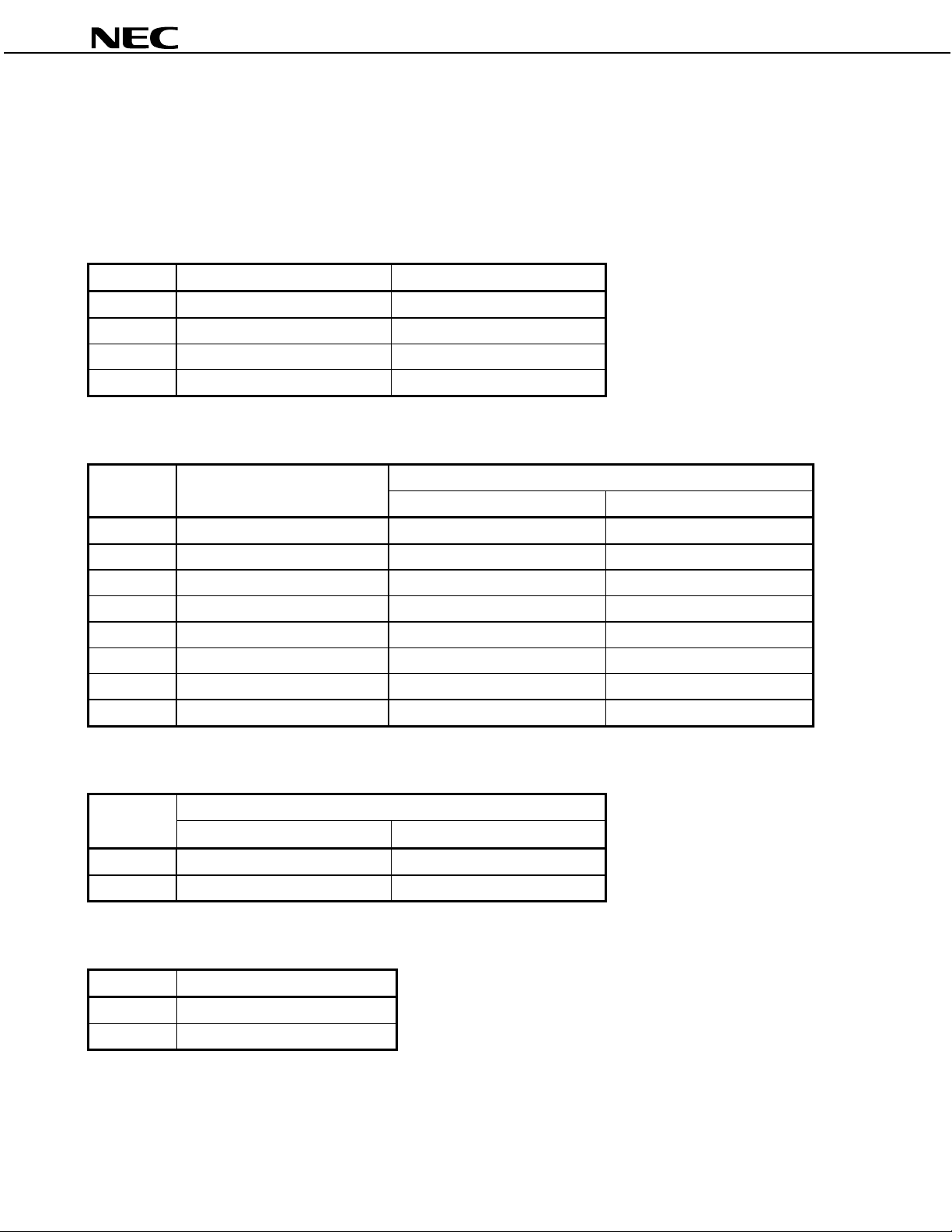
Selection of sampling rate (set via RATE[1:0] bit in register 00h)
RATE [1:0] Sampling Rate In Case of f
00 f
01 f
10 f
11 f
MCLK
/3072 (initial value) 8 kHz
MCLK
/1536 16 kHz
MCLK
/768 32 kHz
MCLK
/512 48 kHz
MCLK
= 24.576 MHz
Selection of audio data format (set via FSDF[2:0] bit in register 01h)
Audio Data Format (2’s Complement, MSB First)FSDS [2:0] Bit Clocks per Frame
PCM Input Data: SI PCM Output: SO
000 64 Left justified Left justified
001 64 Left justified Right justified
010 64 Right justified Left justified
011 64 Right justified Right justified
100 48 Left justified Left justified
101 48 Left justified Right justified
110 48 Right justified Left justified
111 32 (initial value) −−
Selection of LRCLK polarity (set via LRCLKS bit in register 00h)
LRCLK LevelLRCLKS
High Level Low Level
0 L channel (initial value) R channel (initial value)
1 R channel L channel
Selection of LRCLK/BIT_CLK direction (set via CLKIOS bit in register 00h)
CLKIOS LRCLK/BIT_CLK Direction
0 Input (initial value)
1 Output
The µPD63335 can operate in both master mode (the mode in which the µPD63335 outputs LRCLK and
BIT_CLK) and slave mode (the mode in which the µPD63335 is supplied with LRCLK and BIT_CLK externally). Set
the registers related to each mode using the recommended procedure below.
12
Data Sheet S15003EJ6V0DS

µ
PD63335
(1) When using the master mode (LRCLK, BIT_CLK generated internally)
(a) To start ADC, DAC operation from the ADC, DAC power down status (including at power ON)
<1> Set the DAC volume register (10h, 11h) and DAC master volume register (14h, 15h) to MUTE
<2> Set the LRCLK/BIT_CLK operation mode (use the reset/clock status register (00h))
Note 2
Note 1
.
<3> Set the audio format (use the interface/timing register (01h)).
<4> Cancel ADC, DAC power down (use the power down control register (18h)).
<5> Set the DAC volume register (10h, 11h) and the DAC master volume register (14h, 15h)
Note 3
.
(b) To change the LRCLK/BIT_CLK operation mode setting during ADC, DAC operation
<1> Set the DAC volume register (10h, 11h) and the DAC master volume register (14h, 15h) to MUTE
<2> Change the LRCLK/BIT_CLK operation mode setting (use the reset/clock status register (00h)).
<3> Set the audio format (if there is a change) (use the interface/timing register (01h)).
<4> Set the DAC volume register (10h, 11h) and the DAC master volume register (14h, 15h)
Note 5
.
Notes 1. Immediately after canceling ADC, DAC power down, noise may occur in the ADC and DAC
outputs. For this reason, before canceling power down, set the volume for DAC output to
MUTE. (If these volumes are already set to MUTE, at power ON, etc., setting them to MUTE
again is not required.)
2. The LRCLK/BIT_CLK operation mode is set to the slave mode by default. To use it in the
master mode, switch the LRCLK/BIT_CLK operation mode to the master mode while the ADC
and DAC are powered down.
3. To prevent popping noises, after canceling power down and following the lapse of an interval of
time sufficient for three or more LRCLK cycles to be supplied, cancel the MUTE setting of the
volume for the DAC output. Also handle the ADC output data (SO) as valid data once the same
interval of time has elapsed.
4. Immediately after changing the LRCLK/BIT_CLK operation mode, noise may occur in the ADC
and DAC outputs. For this reason, before changing this setting, set the volume for DAC output
to MUTE.
5. To prevent popping noises, after changing the LRCLK/BIT_CLK operation mode, following the
lapse of an interval of time sufficient for three or more LRCLK cycles to be supplied, cancel the
MUTE setting of the volume for the DAC output. Also handle the ADC output data (SO) as valid
data once the same interval of time has elapsed.
.
Note 4
.
Data Sheet S15003EJ6V0DS
13

µ
PD63335
(2) When using the slave mode (LRCLK, BIT_CLK supplied from external)
(a) To start ADC, DAC operation from the ADC, DAC power down status (including at power ON)
<1> Set the DAC volume register (10h, 11h) and DAC master volume register (14h, 15h) to MUTE
<2> Start supplying the external clock (LRCLK, BIT_CLK)
Note 2
.
Note 1
<3> Set the LRCLK/BIT_CLK operation mode (use the reset/clock status register (00h)).
<4> Set the audio format (use the interface/timing register (01h)).
<5> Cancel ADC, DAC power down (use the power down control register (18h)).
<6> Set the DAC volume register (10h, 11h) and the DAC master volume register (14h, 15h)
Note 3
.
(b) To change the LRCLK/BIT_CLK operation mode setting during ADC, DAC operation
<1> Set the DAC volume register (10h, 11h) and the DAC master volume register (14h, 15h) to MUTE
<2> Switch the external clock (LRCLK, BIT_CLK)
Note 5
.
<3> Change the LRCLK/BIT_CLK operation mode setting (use the reset/clock status register (00h)).
<4> Set the audio format (if there is a change) (use the interface/timing register (01h)).
<5> Set the DAC volume register (10h, 11h) and the DAC master volume register (14h, 15h)
Note 6
.
Notes 1. Immediately after canceling ADC, DAC power down, noise may occur in the ADC and DAC
outputs. For this reason, before canceling power down, set the volume for DAC output to
MUTE. (If these volumes are already set to MUTE, at power ON, etc., setting them to MUTE
again is not required.)
2. Start supplying the external clock (LRCLK, BIT_CLK) prior to setting the LRCLK/BIT_CLK
operation mode.
3. To prevent popping noises, after canceling power down and following the lapse of an interval of
time sufficient for three or more LRCLK cycles to be supplied, cancel the MUTE setting of the
volume for the DAC output. Also handle the ADC output data (SO) as valid data once the same
interval of time has elapsed.
4. Immediately after changing the LRCLK/BIT_CLK operation mode, noise may occur in the ADC
and DAC outputs. For this reason, before changing this setting, set the volume for DAC output
to MUTE.
5. Start supplying the external clock (LRCLK, BIT_CLK) immediately it has been changed prior to
changing the LRCLK/BIT_CLK operation mode setting.
6. To prevent popping noises, after changing the LRCLK/BIT_CLK operation mode, following the
lapse of an interval of time sufficient for three or more LRCLK cycles to be supplied, cancel the
MUTE setting of the volume for the DAC output. Also handle the ADC output data (SO) as valid
data once the same interval of time has elapsed.
.
Note 4
.
14
Data Sheet S15003EJ6V0DS

µ
PD63335
(c) To pause supply of the external clock (LRCLK, BIT_CLK) while the power is ON
Power down the ADC and DAC in the sequence described below. To restart the external clock supply,
perform steps <2> to <6> of section (a) To start ADC, DAC operation from the ADC, DAC power down
status (including at power ON).
<1> Set the DAC volume register (10h, 11h) and the DAC master volume register (14h, 15h) to MUTE
<2> Power down the ADC and DAC (use power down control register (18h)).
<3> Stop the external clock (LRCLK, BIT_CLK) (fix it to high level or low level)
Notes 1. Immediately after executing ADC, DAC power down, noise may occur in the ADC and DAC
outputs. For this reason, before executing power down, set the volume for the DAC output to
MUTE.
2. To reliably power down ADC and DAC, following input of the ADC, DAC power down command,
stop supplying the external clock (LRCLK, BIT_CLK) after supplying LRCLK for three cycles or
more.
Note 2
.
Note 1
.
Data Sheet S15003EJ6V0DS
15
µ
PD63335
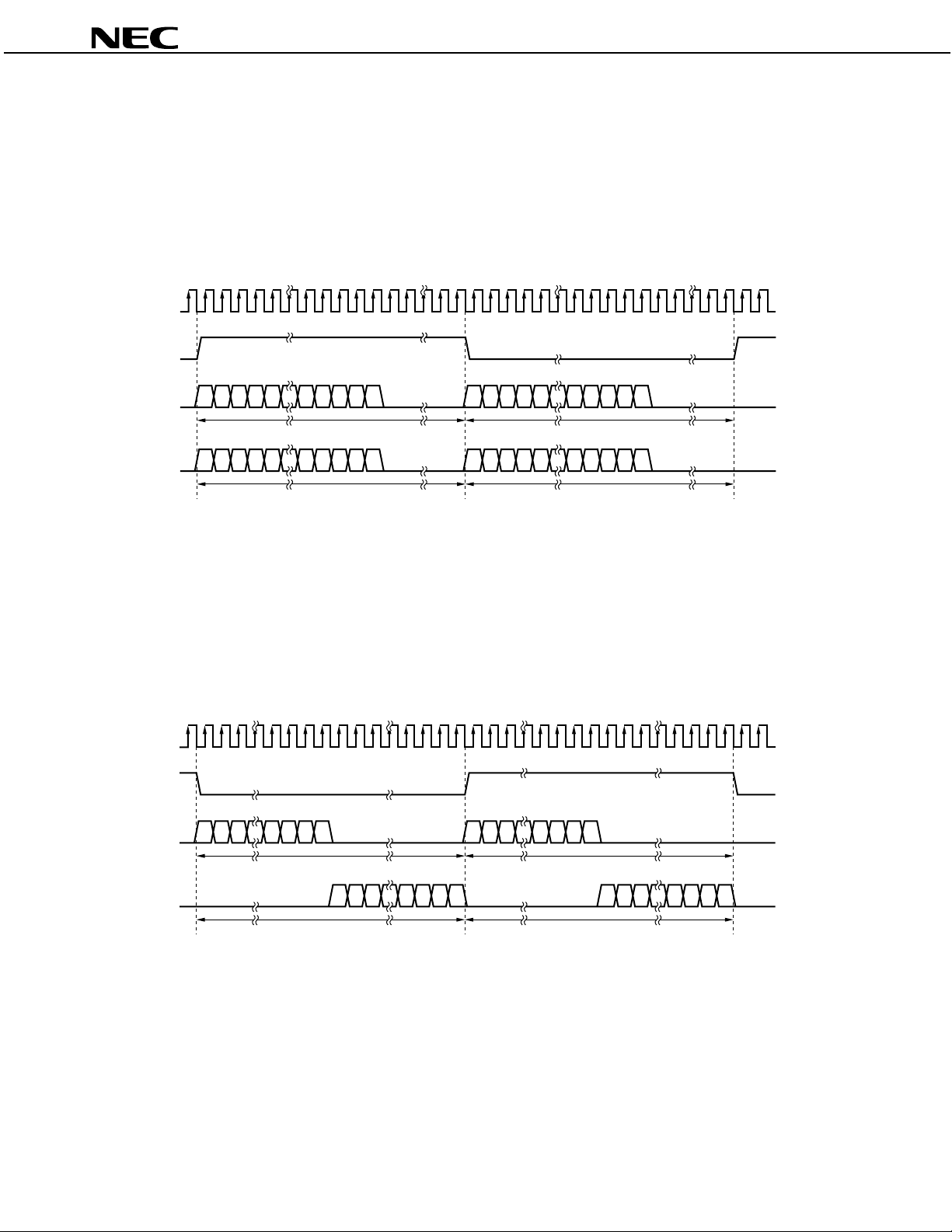
1.6.3 Data format of FSDF2:FSDF1:FSDF0:LRCLKS = 0:0:0:0
• CLKIOS = “0”: Input of both BIT_CLK and LRCLK
• CLKIOS = “1”: Output of both BIT_CLK and LRCLK
• BIT_CLK: 64 fS
• Data I/O occurs via the L channel while LRCLK is at high level and occurs via the R channel while LRCLK is at low
level.
y SI and SO have left-justified data input and output.
BIT_CLK
64 fs
LRCLK
SI
L14 L13 L12 L11 L4 L3 L2 L1 L0
R15 R14 R13 R12 R11
R4 R3 R2 R1 R0L15
Left channel data Right channel data
SO
L14 L13 L12 L11 L4 L3 L2 L1 L0
R15 R14 R13 R12 R11
R4 R3 R2 R1 R0L15
Left channel data Right channel data
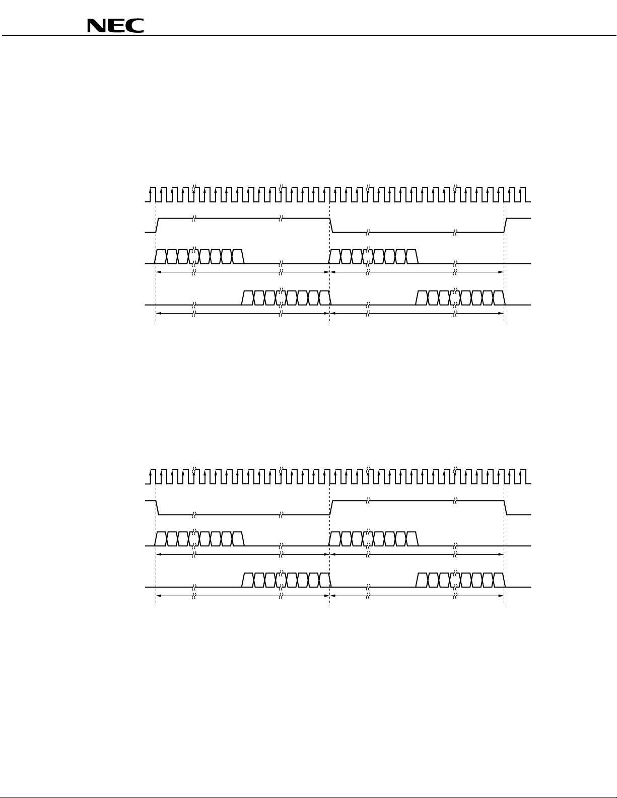
1.6.4 Data format of FSDF2:FSDF1:FSDF0:LRCLKS = 0:0:0:1
• CLKIOS = “0”: Input of both BIT_CLK and LRCLK
• CLKIOS = “1”: Output of both BIT_CLK and LRCLK
• BIT_CLK: 64 f
S
• Data I/O occurs via the R channel while LRCLK is at high level and occurs via the L channel while LRCLK is at low
level.
• SI and SO have left-justified data input and output.
BIT_CLK
64 fs
LRCLK
SI
L14 L13 L3 L1 L0
L2 R2R3
R15 R14 R13
R4
R1 R0L15
16
SO
Left channel data Right channel data
L15 L13 L2 L1 L0
L14
R15
R14L3R13
Left channel data Right channel data
Data Sheet S15003EJ6V0DS
R3R4
R2 R1 R0
µ
PD63335
1.6.5 Data format of FSDF2:FSDF1:FSDF0:LRCLKS = 0:0:1:0
• CLKIOS = “0”: Input of both BIT_CLK and LRCLK
• CLKIOS = “1”: Output of both BIT_CLK and LRCLK
• BIT_CLK: 64 fS
• Data I/O occurs via the L channel while LRCLK is at high level and occurs via the R channel while LRCLK is at low
level.
• SI has left-justified data input and SO has right-justified data output.
BIT_CLK
64 fs
LRCLK
SI
L14 L13 L3 L1 L0
L2 R2R3
R15 R14 R13
R4
R1 R0L15
Left channel data Right channel data
SO
L15 L13 L2 L1 L0
L14
R15
R14L3R13
R3R4
R2 R1 R0
Left channel data Right channel data
1.6.6 Data format of FSDF2:FSDF1:FSDF0:LRCLKS = 0:0:1:1
• CLKIOS = “0”: Input of both BIT_CLK and LRCLK
• CLKIOS = “1”: Output of both BIT_CLK and LRCLK
• BIT_CLK: 64 f
S
• Data I/O occurs via the R channel while LRCLK is at high level and occurs via the L channel while LRCLK is at low
level.
• SI has left-justified data input and SO has right-justified data output.
BIT_CLK
64 fs
LRCLK
SI
L14 L13 L3 L1 L0
L2 R2R3
R15 R14 R13
R4
R1 R0L15
SO
Left channel data Right channel data
L15 L13 L2 L1 L0
L14
R15
R14L3R13
Left channel data Right channel data
Data Sheet S15003EJ6V0DS
R3R4
R2 R1 R0
17
 Loading...