
DATA SHEET
MOS INTEGRATED CIRCUIT
µ
PD63310
STEREO SOUND CODEC
The µPD63310 is an LSI that features two channels each of on-chip 16-bit ADC and DAC circuits for mutual conversion
between digital signals and audio signals (having a maximum signal bandwidth of 24 kHz).
The analog signal input block enables mixed input of four different stereo signals and one monaural signal, and the
µ
volume of each signal can be controlled before mixing. The
(mic amps) and gain is adjustable between 10 and 30 dB.
The analog signal output block enables mixed output of analog signals output by the DAC and four different stereo
analog signals, and the volume of each signal can be controlled before mixing.
The digital audio signal I/O block supports a serial interface for audio applications (two’s complement, MSB first).
A 6-bit parallel port are used for the various volume settings, with volume settings selectable (in 1.5-dB steps) from –
46.5 dB to 0 dB, as well as a mute setting.
PD63310 also features two on-chip microphone amplifiers
FEATURES
• Two channels each of ∆Σ type ADC and DAC
• On-chip mixing circuit in analog I/O block
• Low-noise mic amps for two channels on chip
• On-chip reference voltage power supply (1.4 V TYP.)
• ADC and DAC digital filter characteristics
Pass band ripple : ±0.1 dB (0 to 0.454 fs) for ADC and DAC
Stop band attenuation : 75 dB (0.546 fs or above) for ADC and DAC
• Sampling frequency (fs): 2 to 48 kHz (256-fs master clock is input from an external source)
• Low voltage operation: +3 to +5.5 V single power supply
• Wide operating ambient temperature: –20 to +80°C
• Low power consumption: 120 mW (when using 3-V power supply), 250 mW (when using 5-V power supply)
• 80-pin plastic TQFP
RECOMMENDED USES
• Speech recognition system, including car navigation system
• PC sound system
ORDERING INFORMATION
Part Number Package
µ
PD63310GK-9EU 80-pin plastic TQFP (FINE PITCH) (12 × 12 mm)
Document No. S11319EJ7V0DS00 (7th edition)
Date Published October 1998 N CP(K)
Printed in Japan
The information in this document is subject to change without notice.
The mark shows major revised points.
©
1996
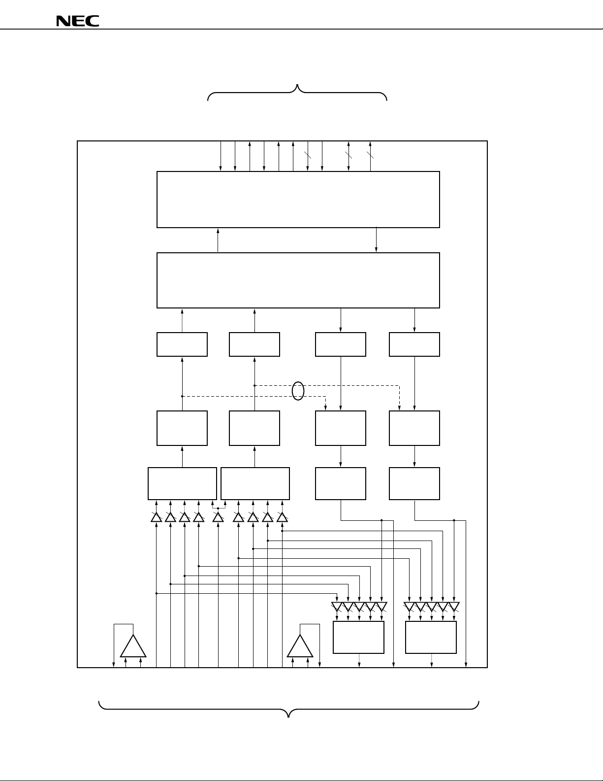
BLOCK DIAGRAM
CSB
Digital I/O terminals
SELRSOSI
BCLK
LRCLK
RB, WB
MCLK
262
I/O interface
Digital filter
DATA5-
DATA0
OEB, RBW
µ
PD63310
Interpolator InterpolatorDecimeterDecimeter
Analog loopback
(for test mode selection)
MIC AMPMIC AMP
DAC DACADCADC
Filter FilterMixerMixer
Mixer Mixer
–+–+
MICPL
MICOL
IN1L
MICNL
IN2L
IN3L
IN4L
IN5
IN1R
IN2R
IN3R
IN4R
Analog I/O terminals
MICPR
MICNR
MICOR
OUTL
DACL
OUTR
DACR
2
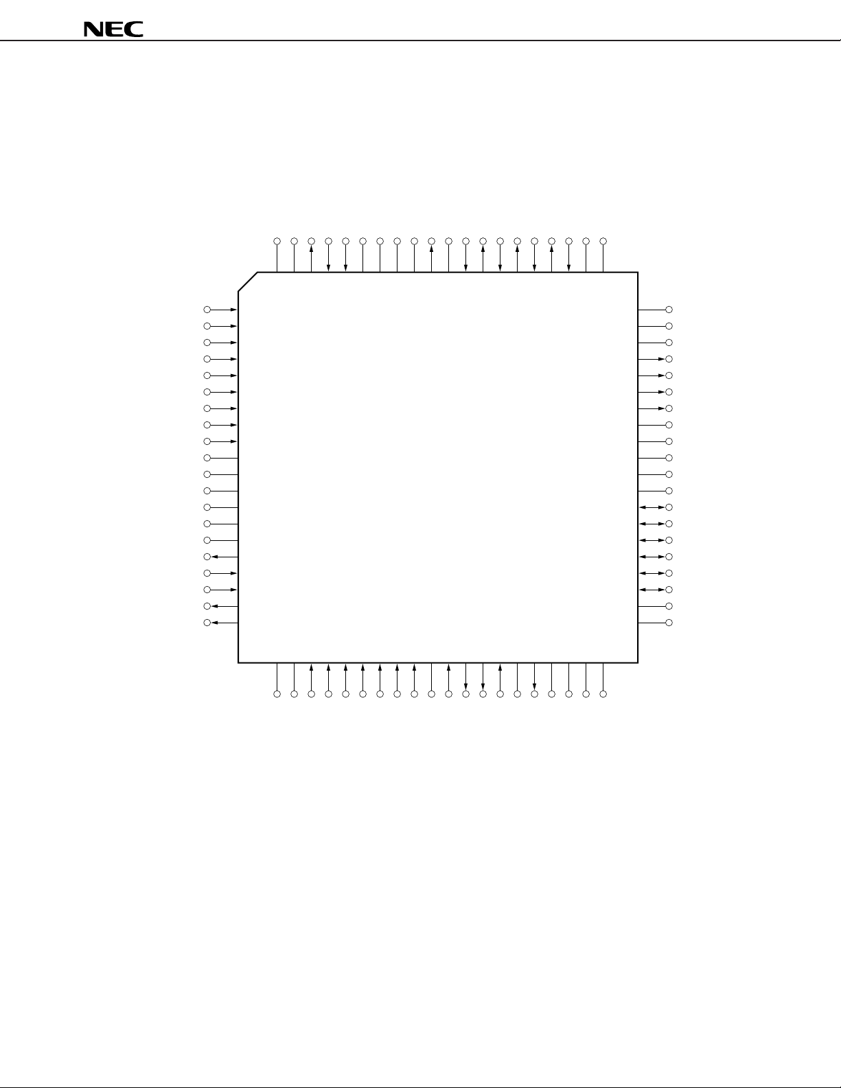
PIN CONFIGURATION (Top View)
80-pin plastic TQFP (FINE PITCH) (12 × 12 mm)
•µPD63310GK-9EU
µ
PD63310
IN1R
IN2R
IN3R
IN4R
IN5
IN4L
IN3L
IN2L
IN1L
NC
NC
NC
NC
NC
NC
MICOL
MICNL
MICPL
RBW
OEB
NCNCMICOR
80 79 78 77 76 75 74 73 72 71 70 69 68 67 66 65 64 63 62 61
1
2
3
4
5
6
7
8
9
10
11
12
13
14
15
16
17
18
19
20
MICNR
MICPR
AGND1
AGND2NCAGND3
VXLONCVXLI
VXRO
VXRI
VRLO
VRLI
VRRO
VRRINCNC
60
59
58
57
56
55
54
53
52
51
50
49
48
47
46
45
44
43
42
41
AVDD
AGND4
AGND5
OUTL
DACL
OUTR
DACR
NC
NC
NC
NC
NC
DATA0
DATA1
DATA2
DATA3
DATA4
DATA5
DGND2
DGND1
21 22 23 24 25 26 27 28 29 30 31 32 33 34 35 36 37 38 39 40
NC
NC
WB
RB
CSB
SELR
TEST1
RSTB
TEST2
NC
MCLK
LRCLK
SI
BCLK
NC
SO
DD
NCNCNC
DV
3
µ
PD63310
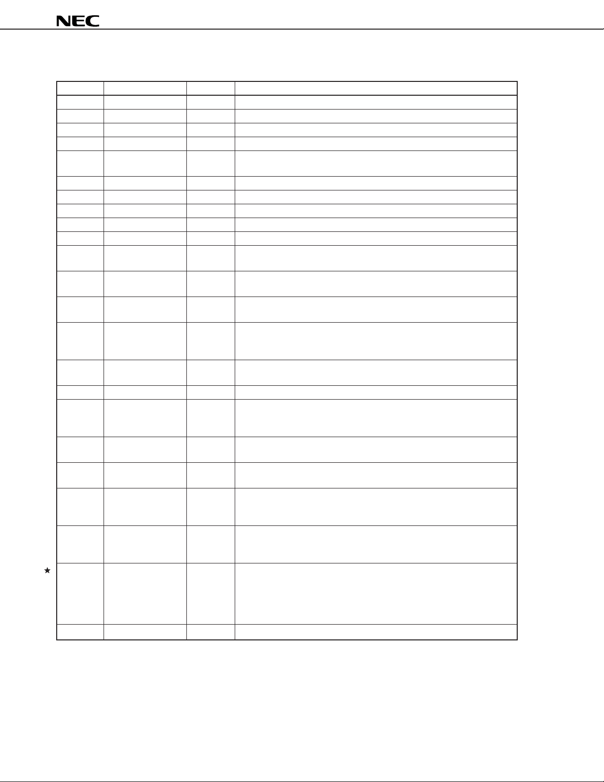
PIN FUNCTIONS
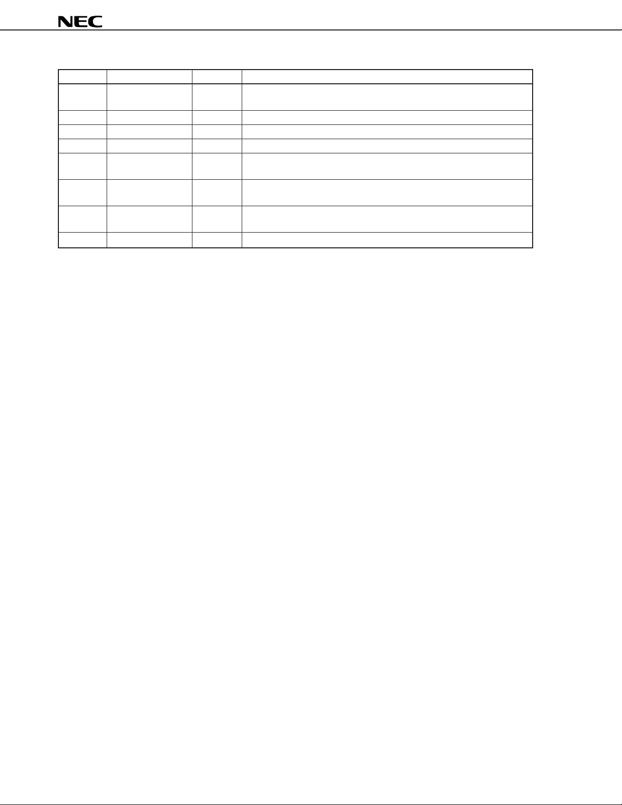
Pin Number Pin Name I/O Function
1 IN1R I R-channel analog audio signal input pin 1
2 IN2R I R-channel analog audio signal input pin 2
3 IN3R I R-channel analog audio signal input pin 3
4 IN4R I R-channel analog audio signal input pin 4
5 IN5 I Analog audio signal (monaural) input pin. This channel accepts audio input
which is input to both left and right channels on the chip.
6 IN4L I L-channel analog audio signal input pin 4
7 IN3L I L-channel analog audio signal input pin 3
8 IN2L I L-channel analog audio signal input pin 2
9 IN1L I L-channel analog audio signal input pin 1
10-15 NC — No connection
16 MICOL O L-channel mic amp output pin. If the L-channel mic amp is not being used,
connect this pin to MICNL pin.
17 MICNL I L-channel mic amp inverting input pin. If the L-channel mic amp is not being
used, connect this pin to MICOL pin.
18 MICPL I L-channel mic amp noninverting input pin. If the L-channel mic amp is not
being used, connect this pin to VXLO pin.
19 RBW O Output pin for signal that specifies the bus driver’s direction. Output is at
high level when DATA5 to DATA0 are input pins and is at low level when
DATA5 to DATA0 are output pins. If not used, leave unconnected.
20 OEB O Bus driver enable signal output pin. When data input to DATA5 to DATA0
is enabled, output is at low level. If not used, leave unconnected.
21, 22 NC — No connection
23 WB I Input pin for parallel interface’s data write signal. Used for input of low-level
signals when addresses are written to the volume setting register and when
data is written.
24 RB I Input pin for parallel interface’s data read signal. Used for input of low-level
signals when data is read from the volume setting register.
25 CSB I Input pin for parallel interface’s chip select signal. Active low. When the
input signal is at high level, DATA5 to DATA0 are set for high impedance.
26 SELR I Input pin for signal that specifies the target register for parallel data input and
output. Specifies an address register when the input signal is at low level,
or a data register when the input signal is at high level.
27, 28 TEST1, TEST2 I Test mode setting pins. These pins set the test mode when at high level.
When not used (i.e., during normal operation mode), connect these pins to
GND.
29 RSTB I Reset signal input pin. A reset occurs when a low pulse (pulse width of 1/
(8 fs) or greater) is input after starting MCLK. The case when a reset is
necessary is not only power-on but also an occurrence of disturbance in
master clock due to changing fS (sampling frequency). When input is at low
level, power down mode is set to reduce power consumption.
30 NC — No connection
(1/3)
4
µ
PD63310
(2/3)
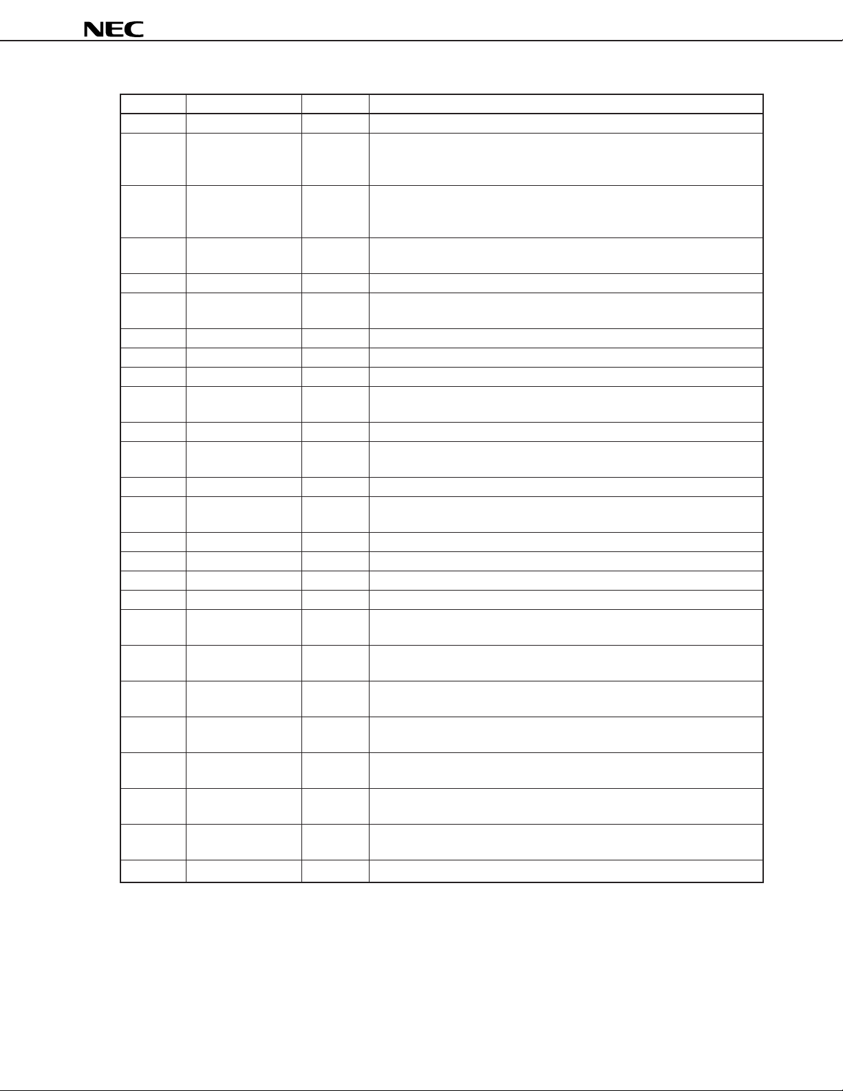
Pin Number Pin Name I/O Function
31 MCLK I Master clock input pin. Used for input of 256-fs clock (duty: 40 to 60%).
32 LRCLK O Serial interface’s frame sync clock output pin.
Used for L channel data I/O when LRCLK = low level
Used for R channel data I/O when LRCLK = high level
33 BCLK O Serial interface’s bit sync clock output pin.
Used for I/O of audio data from SI and SO in sync with BCLK. BCLK is
generated on-chip as MCLK divided by eight.
34 SI I Serial interface’s data input pin. Used for serial input (synchronized with
BCLK) of audio data (two’s complement, MSB first).
35 NC — No connection
36 SO O Serial interface’s data output pin. Used for serial output (synchronized with
BCLK) of audio data (two’s complement, MSB first).
37 DVDD — Digital power supply pin. Used for input voltage range of +3 to +5.5 V.
38-40 NC — No connection
41, 42 DGND1, DGND2 G Digital ground pins.
43-48 DATA5-DATA0 I/O Parallel data I/O pins. Used for input/output of address data and volume
setting data.
49-53 NC — No connection
54 DACR O R-channel DAC output pin. When this pin is used, the R-channel DAC output
can be monitored without attenuation regardless of the volume setting.
55 OUTR O R-channel analog audio output pin.
56 DACL O L-channel DAC output pin. When this pin is used, the L-channel DAC output
can be monitored without attenuation regardless of the volume setting.
57 OUTL O L-channel analog audio output pin.
58, 59 AGND5, AGND4 G Analog ground pins.
60 AVDD — Analog power supply pin. Used for input voltage range of +3 to +5.5 V.
61, 62 NC — No connection
63 VRRI I Reference voltage input pin for R-channel DAC. This pin is usually connected
to VRRO pin.
64 VRRO O Reference voltage output pin for R-channel DAC. Output is 1.4 V (TYP.).
Connects to analog GND via a bypass capacitor.
65 VRLI I Reference voltage input pin for L-channel DAC. This pin is usually connected
to VRLO pin.
66 VRLO O Reference voltage output pin for L-channel DAC. Output is 1.4 V (TYP.).
Connects to analog GND via a bypass capacitor.
67 VXRI I Reference voltage input pin for R-channel ADC. This pin is usually connected
to VXRO pin.
68 VXRO O Reference voltage output pin for R-channel ADC. Output is 1.4 V (TYP.).
Connects to analog GND via a bypass capacitor.
69 VXLI I Reference voltage input pin for L-channel ADC. This pin is usually connected
to VXLO pin.
70 NC — No connection
5
µ
PD63310
(3/3)
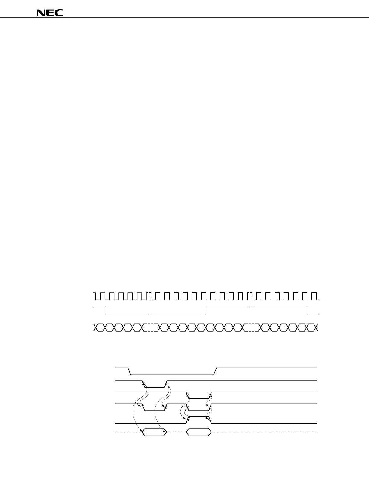
Pin Number Pin Name I/O Function
71 VXLO O Reference voltage output pin for L-channel ADC. Output is 1.4 V (TYP.).
Connects to analog GND via a bypass capacitor.
72 AGND3 G Analog ground pin.
73 NC — No connection
74, 75 AGND2, AGND1 G Analog ground pins.
76 MICPR I R-channel mic amp noninverting input pin. If the R-channel mic amp is not
being used, connect this pin to VXRO pin.
77 MICNR I R-channel mic amp inverting input pin. If the R-channel mic amp is not being
used, connect this pin to MICOR pin.
78 MICOR O R-channel mic amp output pin. If the R-channel mic amp is not being used,
connect this pin to MICNR pin.
79, 80 NC — No connection
6
µ
PD63310
1. DESCRIPTION OF OPERATIONS
1.1 Analog Input Block
The analog input block enables signal input from two channels. Four different stereo signals (IN1 to IN4) and a
monaural signal (IN5) can be mixed and input via these channels. The volume can be adjusted for each analog signal,
and the sum of the volume settings is input to the ADC. A 6-bit signal is used to adjust the volume within an adjustment
range (in 1.5-dB steps) from –46.5 dB to 0 dB, plus a mute setting. A low-noise mic amp (variable gain width: 10 to 30
dB) is provided on-chip for mic input.
1.2 Analog Output Block
The analog output block enables signal output from two channels. Five different analog signals (IN1 to IN4 and DAC)
can be mixed and output via these channels. The volume can be adjusted for each analog signal, and the sum of the
volume settings is output (via OUTL and OUTR pins). A 6-bit signal is used to adjust the volume within an adjustment
range (in 1.5-dB steps) from –46.5 dB to 0 dB, plus a mute setting. The output from the DAC (via DACL and DACR pins)
can be monitored directly.
1.3 Digital Interface
A serial interface for audio is supported for input and output of digital audio data (two’s complement, MSB first).
BCLK and LRCLK are automatically generated on chip from the master clock that is supplied to MCLK pin from an
external source. BCLK and LRCLK are used by the ADC and DAC. In other words, the ADC’s and DAC’s sampling
frequency is determined based on the master clock and cannot be set independently of it.
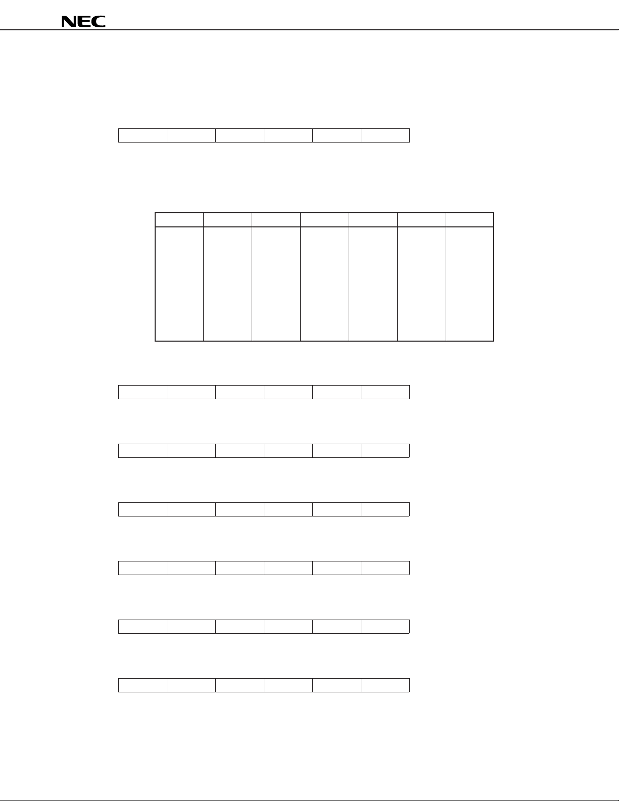
A parallel interface is used for input and output of the 6-bit data used for volume adjustments. The target registers for
parallel data I/O are selected via the SELR pin. This pin selects an address register when at low level and a data register
when at high level.
OEB is output as the bus driver’s enable signal and RBW is output as the bus driver’s direction specification signal.
Use this pin as necessary. If it is not used, leave it unconnected.
When the clock (data) input to the MCLK and SI pins has been stopped, set these pins to either high level or low level
(if necessary, connect via a resistance to DV
DD or DGND).
(1) Serial interface
BCLK
LRCLK
SI, SO 15 14 13 12
(2) Parallel interface
RB
WB
(I)
(I)
(I)
(O)
(O)
(I/O)DATA5-
CSB
OEB
RBW
DATA0
L-channel data
4321015141312
R-channel data
43210
LSB LSB
7

µ
PD63310
1.4 Volume Setting Register Addresses
After the power is turned on and a reset has been input, all volume settings are set to mute mode. Therefore, it may
be necessary to specify volume settings before inputting signals. Write data to the volume setting registers that correspond
to the analog input pins and analog output pins to be used.
Since the ADC’s full scale analog input signal amplitude voltage is 1.4 V (TYP.), it may be necessary to specify a
volume setting whereby the signal amplitude’s maximum voltage (after mixing) is no more than 1.4 V, especially when
several analog signals are input to the ADC after mixing.
The addresses of the various volume setting registers are specified via the 6-bit parallel data that is input from the
DATA5 to DATA0 pins during low-level input to the SELR pin. The volume setting registers corresponding to these
addresses are listed below.
0 : IN1L control register
1 : IN1R control register
2 : IN2L control register
3 : IN2R control register
4 : IN3L control register
5 : IN3R control register
6 : IN4L control register
7 : IN4R control register
8 : IN5 control register
9 : IN1L-OUTL control register
10 : IN1R-OUTR control register
1 1 : IN2L-OUTL control register
12 : IN2R-OUTR control register
13 : IN3L-OUTL control register
14 : IN3R-OUTR control register
15 : IN4L-OUTL control register
16 : IN4R-OUTR control register
17 : DACL-OUTL control register
18 : DACR-OUTR control register
8
µ
PD63310
1.5 Volume Setting Register Data (Command Types)
The data in the volume setting registers is written and read based on 6-bit parallel data that is input and output via the
DATA5 to DA T A0 pins when the SELR pin is set for high level input. The data (commands) in the various volume setting
registers are described below.
0: D5 D4 D3 D2 D1 D0
D4 to D0 indicate the data used to control gain in the IN1L register’s input signal, with codes corresponding
to the gain levels listed in Table 1-1 below. When D5 is “1”, mute mode is set.
Table 1-1. Correspondence of Codes and Gain Levels
D5 D4 D3 D2 D1 D0 Gain
0000000 dB
000001–1.5 dB
000010–3.0 dB
|||||||
011110–45.0 dB
011111–46.5 dB
100000MUTE
1 ЧЧЧЧЧMUTE
Note Default value
Remark × : Don’t care
Note
1: D5 D4 D3 D2 D1 D0
D4 to D0 indicate the data used to control gain in the IN1R register’s input signal, with codes corresponding
to the gain levels listed in Table 1-1. Mute mode is set when D5 = 1.
2: D5 D4 D3 D2 D1 D0
D4 to D0 indicate the data used to control gain in the IN2L register’s input signal, with codes corresponding
to the gain levels listed in Table 1-1. Mute mode is set when D5 = 1.
3: D5 D4 D3 D2 D1 D0
D4 to D0 indicate the data used to control gain in the IN2R register’s input signal, with codes corresponding
to the gain levels listed in Table 1-1. Mute mode is set when D5 = 1.
4: D5 D4 D3 D2 D1 D0
D4 to D0 indicate the data used to control gain in the IN3L register’s input signal, with codes corresponding
to the gain levels listed in Table 1-1. Mute mode is set when D5 = 1.
5: D5 D4 D3 D2 D1 D0
D4 to D0 indicate the data used to control gain in the IN3R register’s input signal, with codes corresponding
to the gain levels listed in Table 1-1. Mute mode is set when D5 = 1.
6: D5 D4 D3 D2 D1 D0
D4 to D0 indicate the data used to control gain in the IN4L register’s input signal, with codes corresponding
to the gain levels listed in Table 1-1. Mute mode is set when D5 = 1.
9
 Loading...