
DATA SHEET
MOS INTEGRATED CIRCUIT
µ
PD63210,63210L
16-BIT D/A CONVERTER WITH BUILT-IN DIGITAL FILTER FOR AUDIO
DESCRIPTION
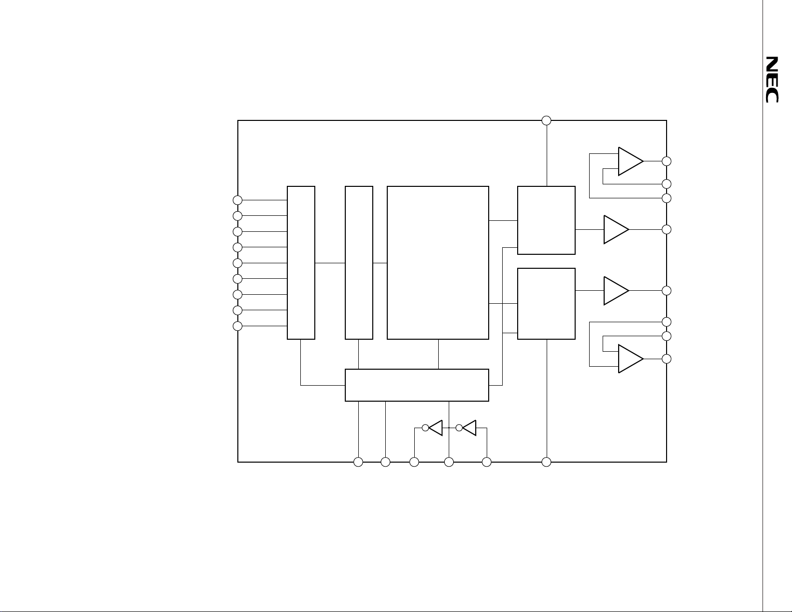
The µPD63210 is a 16-bit dual D/A converter IC for digital audio demodulation, which incorporates an 8-times
oversampling digital filter and operational amplifiers for analog post filters. With few external parts and an easy
substrate design (as to 1-bit D/A), it is suitable for multimedia terminals, MPEG audio equipment, video CDs, game
machines, and electronic musical instruments, etc. To cope with sets for portable applications, a low-voltage operating
version µPD63210L (lowest operating supply voltage = +3.0 V) is also available.
FEATURES
• 16-bit resistor string D/A converter (2-channel) adopted
S/N = 104 dBTYP.; DR = 96 dBTYP. (when VDD = 5.0 V)
• High-performance 8-times oversampling digital filter incorporated
Pass band ripple : ±0.003 dB
Stop band rejection : 90 dB
• System clock 384/512fs selectable
• Serial input data format selectable
Format for 2’S compliment, MSB first, and backward justification data accommodated;
Input can be selected between 16- and 18 bits
• Full line of low-voltage operating products (
µPD63210 : VDD = 4.5 to 5.5 V
µPD63210L : VDD = 3.0 to 5.5 V
• Wide operating temperature range (T
• Operational amplifier (2-channel) for D/A converter output incorporated
• Operational amplifier (2-channel) for post filter (LPF) configuration incorporated
• Digital de-emphasis function (fs = 32/44.1/48 kHz) incorporated
• Soft mute function incorporated
• CD double-speed playback function (when
• 28-pin plastic SOP (375 mil) adopted
µ
PD63210L)
A = –40 to +85 °C)
µ
PD63210: 384fs)
ORDERING INFORMATION
Part Number Package Quality Grade
µ
PD63210GT 28-pin plastic SOP (375 mil) Standard
µ
PD63210LGT 28-pin plastic SOP (375 mil)
The information in this document is subject to change without notice.
Document No. S11585EJ2V1DS00 (2nd edition)
(Previous No. ID-3466)
Date Published September 1996 P
Printed in Japan
©
1996
2
LREF RREF
+
AOL
ANIL
APIL
LO
RO
APIR
ANIR
AOR
BCKI
SDI
LRCKI
DEFS1
DEFS2
CKSEL
SMUTE
BSEL
TSEL
Input interface circuit
Deemphasis circuit
D/A converter
(L-channel)
8-times oversampling digital filter
D/A converter
(R-channel)
-
Resistor strings
Resistor strings
-
+
BLOCK DIAGRAM
RST
Timing generator
MCKO
DSEL
XTO
µ
PD63210, 63210L
XTI
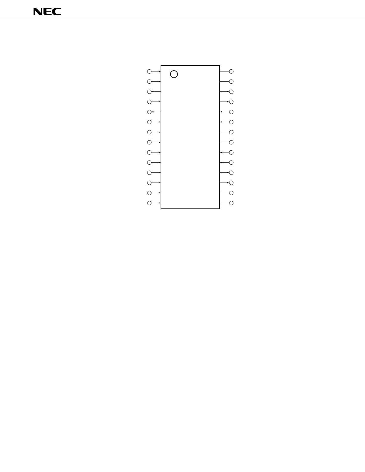
PIN CONFIGURATION (Top View)
µ
PD63210, 63210L
TSEL 1 28 DV
RST 2 27 AV
XTO 3 26 LO
XTI 4 25 AOL
MCKO 5 24 ANIL
CKSEL 6 23 APIL
BCKI 7 22 LREF
SDI 8 21 RREF
LRCKI 9 20 APIR
DEFS1 10 19 ANIR
DEFS2 11 18 AOR
DSEL 12 17 RO
SMUTE 13 16 AGND
BSEL 14 15 DGND
TSEL : Test selection input
RST : Reset input
XTO : Oscillation part output pin
XTI : Oscillation part input pin
MCKO : Master clock output
CKSEL : Clock selection input
BCKI : Bit clock input
SDI : Serial data input
LRCKI : LR clock input
DEFS1 : De-emphasis select input 1
DEFS2 : De-emphasis select input 2
DSEL : Double-speed playback select input
SMUTE : Soft mute control input
BSEL : Data bit count select input
DD
DD
DGND : Digital ground
AGND : Analog ground
RO : D/A converter output (R channel)
AOR : Filter amplifier output (R channel)
ANIR : Filter amplifier inverting input (R channel)
APIR : Filter amplifier non-inverting input (R channel)
RREF : Reference (R channel)
LREF : Reference (L channel)
APIL : Filter amplifier non-inverting input (L channel)
ANIL : Filter amplifier inverting input (L channel)
AOL : Filter amplifier output (L channel)
LO : D/A converter output (L channel)
DD : Analog power supply
AV
DVDD : Digital power supply
3
1. PIN FUNCTIONS
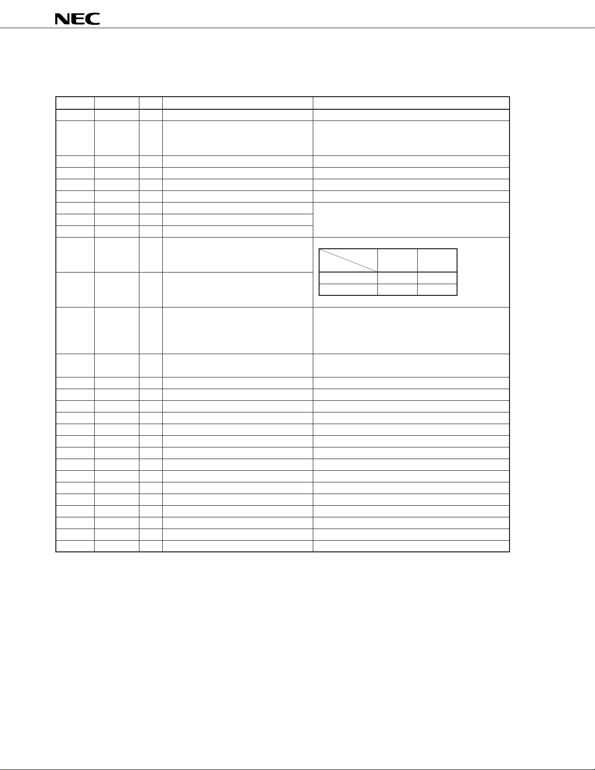
Table 1-1. List of Pin Functions
µ
PD63210, 63210L
Pin No.
1
2
3
4
5
6
7
8
9
10
11
12
13
14
15
16
17
18
19
20
21
22
23
24
25
26
27
28
Symbol
TSEL
RST
XTO
XTI
MCKO
CKSEL
BCKI
SDI
LRCKI
DEFS1
DEFS2
DSEL
SMUTE
BSEL
DGND
AGND
RO
AOR
ANIR
APIR
RREF
LREF
APIL
ANIL
AOL
LO
AVDD
DVDD
I/O
I
Test selection
I
Reset pin
O
Oscillation part output pin
I
Oscillation part input pin
O
Master clock output
I
Clock selection
I
Bit clock input
I
Data input
I
LR clock input
I
De-emphasis switching 1
I
De-emphasis switching 2
I
Double-speed playback switching
Soft mute selection
I
Bit selection
I
Digital GND
Analog GND
DAC output Rch
O
Filter amplifier output Rch
O
Filter amplifier inverting input Rch
I
Filter amplifier non-inverting input Rch
I
Rch reference pin
Lch reference pin
Filter amplifier non-inverting input Lch
I
Filter amplifier inverting input Lch
I
Filter amplifier output Lch
O
DAC output Lch
O
Analog VDD
Digital VDD
-
Function
Description
Normal operation: L
H: System reset
“H” period > 1/128fs
Example: 0.18 µs or more when fs = 44.1 kHz
H: 512fs, L: 384fs
Refer to timing chart
DEFS2
DEFS1
L
H
H: Double speed accommodated; L: Normal
“H” can be selected only when using the µPD63210GT
in 384fs mode (CKSEL = L) (double-speed operation
assured).
Attenuated at the rising edge. Amplified at the trailing
edge. MUTE OFF at “L”.
H: 18 bits; L: 16 bits
L
OFF
48.0 kHz
H
44.1 kHz
32.0 kHz
4
µ
PD63210, 63210L
2. ELECTRICAL SPECIFICATIONS
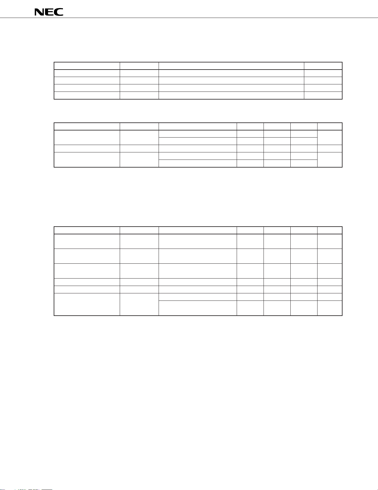
Absolute Maximum Ratings (TA = 25 °C, DGND = AGND = 0V unless otherwise specified)
Parameter
Supply voltage
Input voltage
Permissive dissipation
Storage temperature
Recommended Operating Range (DGND = AGND = 0V)
Symbol
DVDD, AVDD
VIN
PD
Tstg
Rating
–0.3 to +7.0
–0.3 to DVDD +0.3
285 (Ta = 85 °C)
–40 to +125
Unit
V
V
mW
°C
Parameter
Supply voltage
Operating temperature
Output load resistance
Symbol
DVDD, AVDD
Topt
RL
ELECTRICAL SPECIFICATIONS
DC Characteristics (
µ
PD63210: DVDD = AVDD = 4.5 to 5.5 V, DGND = AGND = 0 V, Ta = –40 to +85 °C unless
otherwise specified)
(µPD63210L: DVDD = AVDD = 3.0 to 5.5 V, DGND = AGND = 0 V, Ta = –40 to +85 °C unless
otherwise specified)
Parameter
High-level input voltage
Low-level input voltage
Input leakage current
High-level output voltage
Low-level output voltage
Current consumption
(total)
Symbol
VIH
VIL
VOH
VOL
IDD
Condition
µ
PD63210
µ
PD63210L
µ
PD63210; 17,18,25,26 pins
µ
PD63210L; 17,18,25,26 pins
Condition
1, 2, 6, 7, 8, 9, 10, 11, 12, 13,
and 14 pins
1, 2, 6, 7, 8, 9, 10, 11, 12, 13,
and 14 pins
IL
1, 2, 6, 7, 8, 9, 10, 11, 12, 13,
and 14 pins, Ta = 25 °C
5 pin, IOH = –2.0 mA
5 pin, IOL = 2.0 mA
DVDD = AVDD = 5.0 V
DVDD = AVDD = 3.3 V
(µPD63210L)
MIN.
4.5
3.0
–40
5
10
MIN.
0.7DVDD
–1.2
DVDD–0.4
TYP.
5.0
3.3
+25
TYP.
–
24
14
MAX.
5.5
5.5
+85
MAX.
0.3DVDD
+1.2
+0.4
50
50
Unit
V
°C
kΩ
Unit
V
V
µ
A
V
V
mA
mA
5
µ
PD63210, 63210L
AC Characteristics (µPD63210: DVDD = AVDD = 4.5 to 5.5 V, DGND = AGND = 0 V, Ta = –40 to +85 °C unless
otherwise specified)
(µPD63210L: DVDD = AVDD = 3.0 to 5.5 V, DGND = AGND = 0 V, Ta = –40 to +85 °C unless
otherwise specified)
Parameter
Oscillator frequency
Master clock frequency
Master clock pulse width
(“H” section)
Master clock pulse width
(“L” section)
BCK pulse width
(“H” section)
BCK pulse width
(“L” section)
BCK pulse cycle
Data setup time
Data hold time
LRCK setup time
LRCK hold time
SMUTE pulse width
(“H” section)
Symbol
fX
fMCK
tMWH
tMWL
tBWH
tBWL
tBW
tDS
tDH
tLRS
tLRH
tSMWH
Condition
Crystal oscillation: 384fs;
512fs
External clock input: 384fs;
512fs
External clock input: 384fs;
512fs
External clock input: 384fs;
512fs
MIN.
10
10
10
10
25
19
25
19
150
150
310
100
100
100
100
8/fs
TYP.
16.9344
22.5792
16.9344
22.5792
MAX.
19.2
25.6
19.2
25.6
Unit
MHz
MHz
MHz
MHz
ns
ns
ns
ns
ns
ns
ns
ns
ns
ns
ns
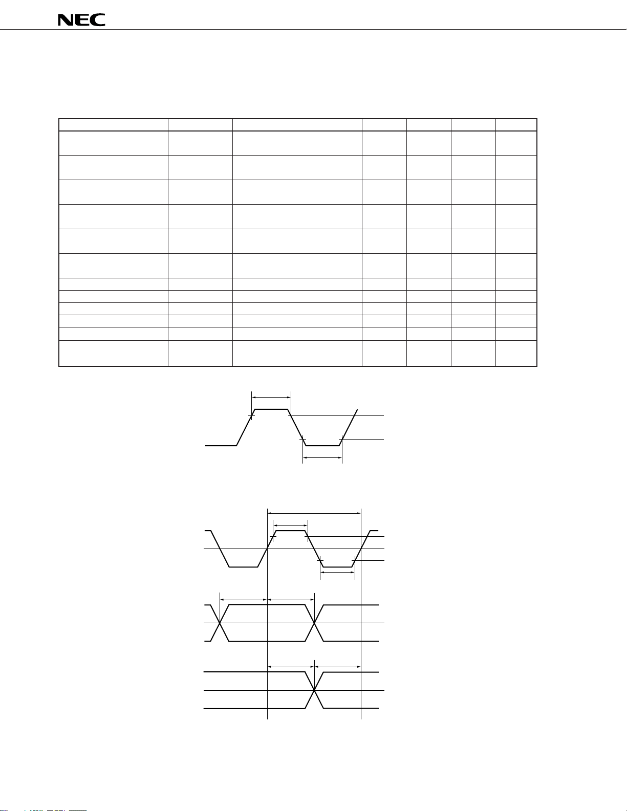
XTI
BCKI
SDI
t
MWH
V
IH
V
IL
t
MWL
t
BW
t
BWH
V
IH
0.5 * DV
V
t
BWL
t
DS
t
DH
0.5 * DV
t
LRH
t
LRS
DD
IL
DD
LRCKI
0.5 * DV
DD
6
 Loading...