NEC UPC2807W Datasheet

DATA SHEET
BiCMOS INTEGRATED CIRCUIT
µ
µ
PC2807,2807A
µ µ
PREAMPLIFIER FOR INFRARED REMOTE CONTROLLER
DESCRIPTION
The µ PC2807 and 2807A are semiconductors integrated circuit developed as preamplifiers for the receiver module of
infrared remote controllers. These preamplifiers can be directly connected to a PIN photodiode, and integrate a high-gain
first stage amplifier, limiter, bandpass filter, detector circuit, and waveform-shaping circuit on a single chip.
FEATURES
• Only PIN photodiode required as an external component.
) selectable (five types):
• Following carrier frequencies (f
PC2807 : fO = 32.7, 36.0, 36.7, 37.9 kHz
µ
PC2807A : fO = 40.0 kHz
µ
• Fixed trap frequency
= 54 kHz
T
f
• Active-low output
• Supplied in form of wafer
APPLICATION
• Receiver module of infrared remote controller
ORDERING INFORMATION
Part Number Condition in shipment
PC2807W Wafer
µ
PC2807AW Wafer
µ
Contact an NEC sales representative in advance since a memorandum on product quality need to be prepared for
O
shipment in the form of wafer.
The information in this document is subject to change without notice. Before using this document, please
confirm that this is the latest version.
Not all devices/types available in every country. Please check with local NEC representative for
availability and additional information.
Document No. S13198EJ1V0DS00 (1st edition)
Date Published May 2000 NS CP (K)
Printed in Japan
The mark ★ shows major revised points.
1998, 2000

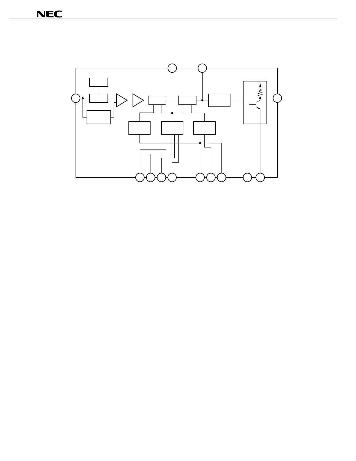
BLOCK DIAGRAM
µ
µ
PC2807, 2807A
µ µ
V
CC
PAD1
6
ABLC
First-stage
amplifier
9
IN
I/V
Carrier
elimination
Limiter
amplifier
TRAP
skip
13
PAD5
TRAP
Trimming
circuit
12 11 10
PAD4
PAD3
BPF
3
fO setting
4
S3 S2
Detector
2
1
S1
Waveform-shaping
circuit
22 kΩ
5 OUT
8 7
GND2PAD6
GND1
2
Data Sheet S13198EJ1V0DS00

µ
µ
PC2807, 2807A
µ µ
PAD FUNCTION
Symbol Pad No. Function
V
CC
GND1 7 GND pad (for output transistor)
GND2 8 GND pad (for circuits excluding output transistor)
IN 9 Input pad. Internal impedance is 190 kΩ TYP. PIN photodiode can be directly connected.
OUT 5
S1 1
S2 2
S3 4
PAD1 3 BPF output pad. Parameters such as voltage gain and BPF bandwidth can be tested.
PAD3 10
PAD4 11
PAD5 12
PAD6 13
6 Power pad. Apply a voltage of 5 V ± 10 %. Connect an external smoothing filter if noise on power line
is high.
Output pad. Open-collector output with pull-up resistor (22 kΩ TYP.) To connect pull-up resistor, use
resistor of 10 kΩ or higher.
BPF center frequency setting pads.
Connect pad corresponding to carrier frequency to be used to GND
Do not connect this pad to anything on final assembly.
Test and trimming pads. Do not connect these pads to anything.
Note
.
Note
Connect each of BPF center frequency setting pads as follows depending on the carrier frequency.
• µ PC2807
Carrier Frequency S1 S2 S3
32.7 kHz GND Leave unconnected. Leave unconnected.
36.0 kHz GND GND GND
36.7 kHz Leave unconnected. GND GND
37.9 kHz Leave unconnected. Leave unconnected. Leave unconnected.
PC2807A
•
µ
Carrier Frequency S1 S2 S3
40.0 kHz Leave unconnected. Leave unconnected. Leave unconnected.
Data Sheet S13198EJ1V0DS00
3
 Loading...