NEC UPC2794GS-E1, UPC2794GS Datasheet

DATA SHEET
BIPOLAR ANALOG INTEGRATED CIRCUIT
µ
PC2794GS
FREQUENCY DOWN CONVERTER FOR
VHF TO UHF BAND TV/VCR TUNER
DESCRIPTION
The µPC2794GS is a Silicon monolithic IC designed for TV/VCR tuner applications. This IC consists of a double
balanced mixer (DBM), local oscillator, preamplifier for precscaler operation, IF amplifier, regulator, UHF/VHF
switching circuit, and so on. This one-chip IC covers a wide frequency band from VHF to UHF bands. This IC is
packaged in 20-pin SOP (Small Outline Package) suitable for surface mounting.
FEATURES
• VHF to UHF bands operation.
• Low distortion CM: VHF (@fRF = 470 MHz) 96 dB
UHF (@fRF = 890 MHz) 92 dB
• Supply voltage : 9 V
• Packaged in 20-pin SOP suitable for surface mounting
µ
µ
ORDERING INFORMATION
Part Number Package Package Style
µ
PC2794GS-E1 20-pin plastic SOP (300 mil) Embossed tape 24 mm wide. 2.5 k/REEL.
Pin 1 indicates pull-out direction of tape
For evaluation sample order, please contact your local NEC office. (Part number for sample order: µPC2794GS)
The information in this document is subject to change without notice. Before using this document, please
confirm that this is the latest version.
Not all devices/types available in every country. Please check with local NEC representative for availability
and additional information.
Document No. P11888EJ3V0DS00 (3rd edition)
Date Published October 1999 N CP(K)
Printed in Japan
Caution electro-static sensitive device
The mark shows major revised points.
©
1996,1999

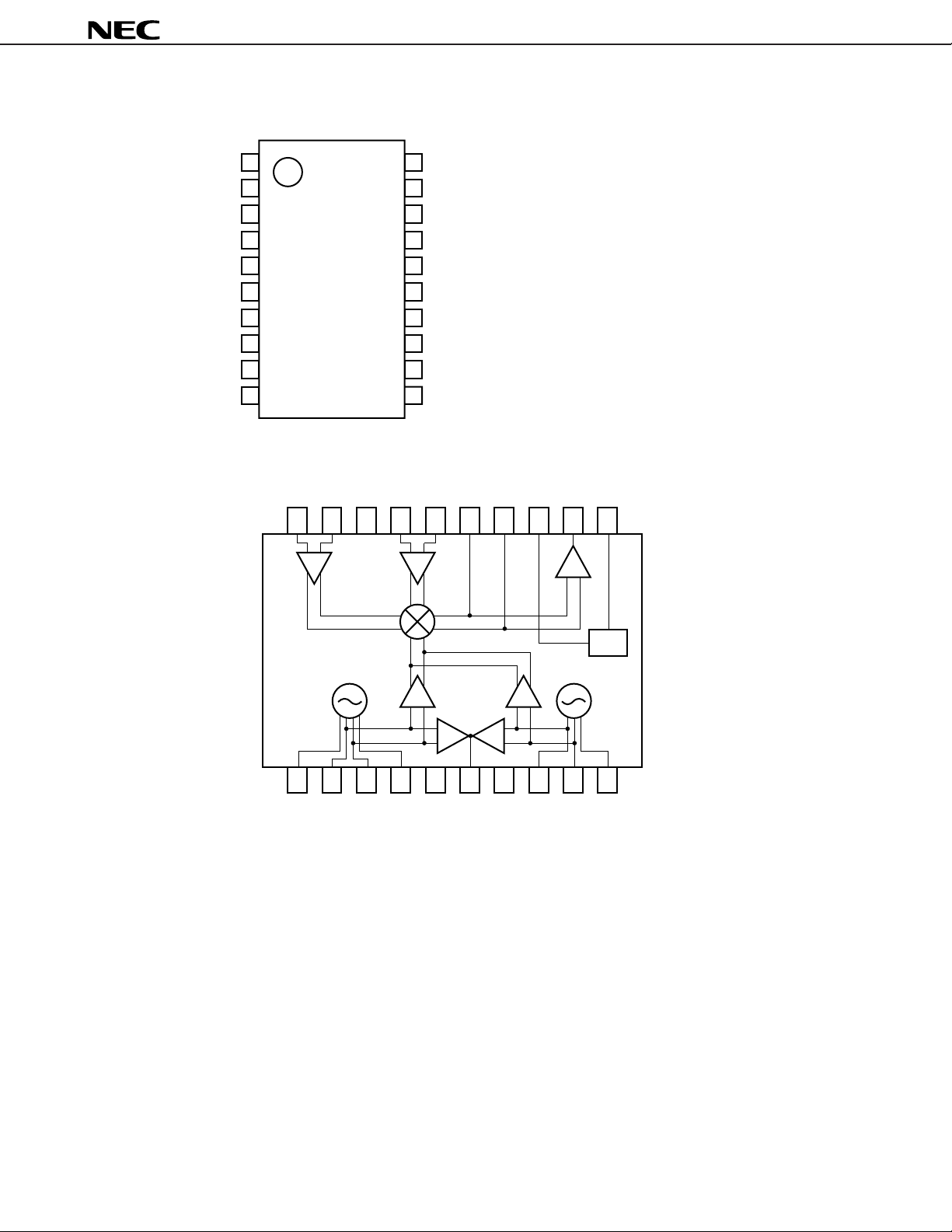
PIN CONFIGURATION (Top View)
µ
PC2794GS
1
10
INTERNAL BLOCK DIAGRAM
20 19 18 17 16 15 14 13 12 11
20
11
UHF OSC Collector
1.
UHF OSC Base
2.
UHF OSC Base
3.
UHF OSC Collector
4.
UB
5.
OSC OUTPUT
6.
GND
7.
VHF OSC Base
8.
VHF OSC Base
9.
VHF OSC Collector
10.
REG
11.
IF OUTPUT
12.
V
13.
CC
14.
MIX OUTPUT
15.
MIX OUTPUT
16.
VHF RF INPUT
17.
VHF RF INPUT
18.
GND
19.
UHF RF INPUT
20.
UHF RF INPUT
IF
Amp
(Tr. 1)
(Tr. 2)
(Tr. 1)
(Tr. 2)
(Tr. 1)
(Tr. 2)
(Tr. 1)
REG.
V OSCU OSC
12345678910
2
Data Sheet P11888EJ3V0DS00

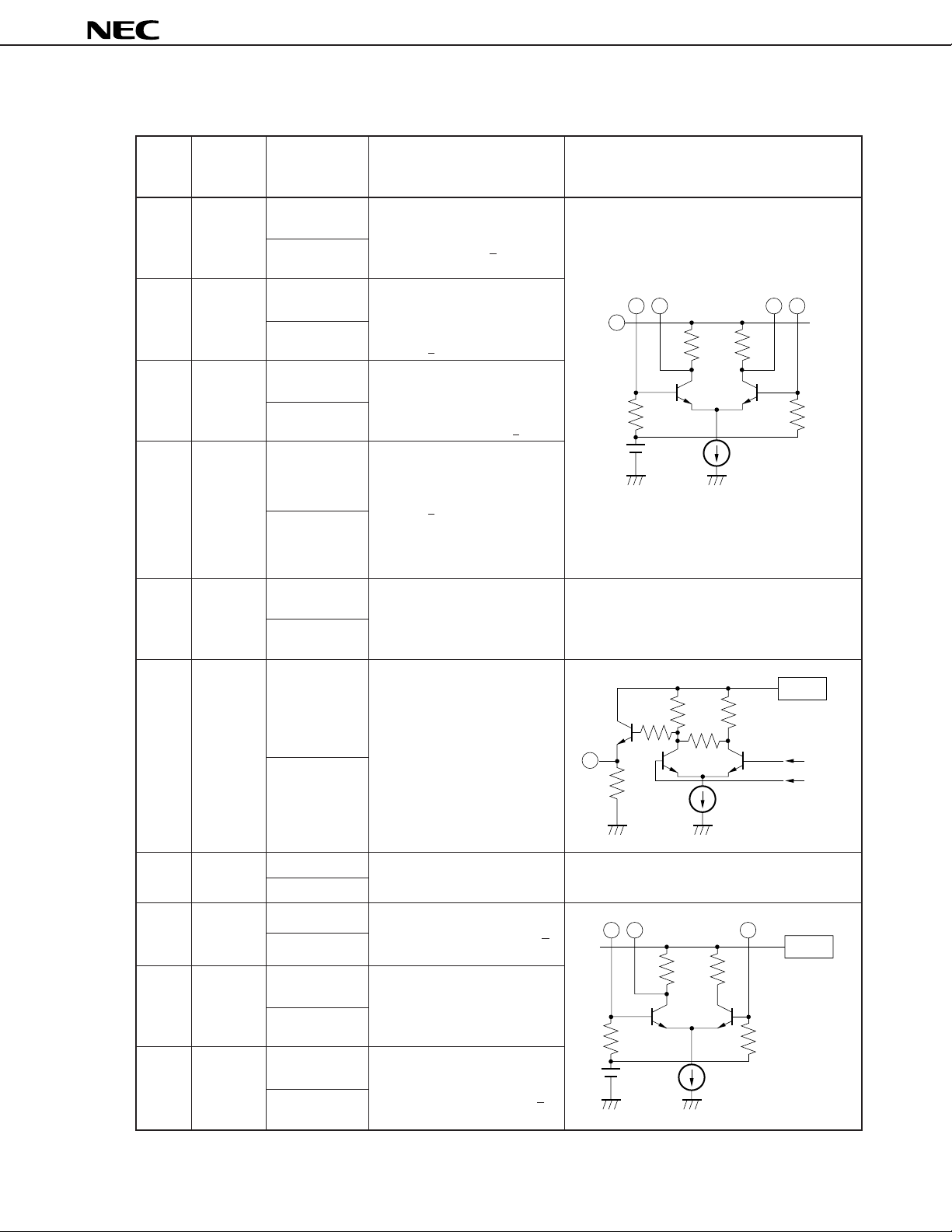
PIN EXPLANATION
Pin Voltage TYP.
Pin No. Symbol
1 UOSC 6.90
collector Assemble LC resonator with 2
(Tr. 1)
2 UOSC 6.00
base (Tr. 2) with balance amplifier. Connected
3
UOSC
base (Tr. 1)
4 UOSC 6.90
collector
(Tr. 2)
5 UB — Switching pin for VHF or UHF
6 OSC 5.40 UHF and VHF oscillator output
output pin. In case of F/S tuner
above: VHF mode
below: UHF mode
6.25
3.90
6.00
3.90
6.25
9.0
Function and Explanation Equivalent Circuit
Collector pin of UHF oscillator.
pin through capacitor ~ 1 pF to
oscillate with active feedback loop.
Base pin of UHF oscillator
to LC resonator through feedback
capacitor ~ 300 pF.
Base pin of UHF oscillator
with balance amplifier.
Connected to LC resonator
through feedback capacitor ~ 300 pF.
Collector pin of UHF oscillator
with balance amplifier. Assemble
LC resonator with 3 pin through
capacitor ~ 1 pF to oscillate with
active feedback loop.
Double balanced oscillator with
transistor 1 and transistor 2.
operation.
VHF operation = open
UHF operation = 9.0 V
application, connected PLL
symthesizer IC’s input pin.
µ
PC2794GS
4 213
5
REG
5.40
7 GND 0.0 GND pin of VHF and UHF
0.0
8 VOSC 3.50 Base pin of VHF oscillator.
base Grounded through capacitor
(Tr. 1)
9 VOSC 3.50 Base pin of VHF oscillator.
base Assemble LC resonator with
(Tr. 2)
10 VOSC 6.20 Collector pin of VHF oscillator.
collector Connected to LC resonator
(Tr. 1)
5.90
5.90
6.90
oscillator.
10 pF.
10 pin to oscillate with active
feedback loop.
through feedback capacitor ~
3 pF.
Data Sheet P11888EJ3V0DS00
6
8
~
10
9
REG
from
OSC
3

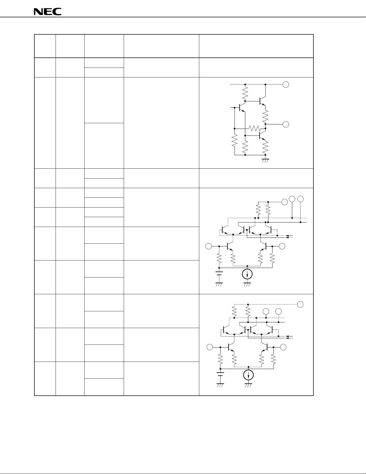
Pin Voltage TYP.
Pin No. Symbol
above: VHF mode
Function and Explanation Equivalent Circuit
below: UHF mode
11 REG 6.90 Monitor pin of regulator output
6.90
voltage.
12 IF output 2.60 IF output pin of VHF-UHF
band functions.
µ
PC2794GS
13
2.60
13 VCC 9.0 Power supply pin for VHF-
9.0
14 MIX 7.10
output1
7.00
15 MIX 7.10
output2
7.00
UHF band functions.
VHF and UHF MIX output pins
These pins should be
equipped with tank circuit to
adjust intermediate frequency.
16 VRF input 2.75 Bypass pin for VHF MIX input.
(bypass) Grounded through capacitor.
2.80
17 VRF input 2.75 VRF signal input pin from
antenna.
2.80
12
.
14 15
13
from
VHF
17
OSC
16
18 GND 0.0 GND pin of MIX, IF amplifier
and regulator.
0.0
19 URF input – Bypass pin for UHF MIX input.
(bypass) Grounded through capacitor.
2.65
20 URF input – URF signal input pin from
antenna.
2.65
4
Data Sheet P11888EJ3V0DS00
19
14 15
20
13
from
UHF
OSC

µ
PC2794GS
ABSOLUTE MAXIMUM RATINGS (TA = 25 °C unless otherwise specified)
Parameter Symbol Condition Rating Unit
Supply Voltage 1 VCC 11.0 V
Supply Voltage 2 UB 11.0 V
Power dissipation PD TA = 80 °C*
Operating ambient temperature TA –40 to +80 °C
Storage temperature Tstg –60 to +150 °C
1
700 mW
*1 Mounted on 50 × 50 × 1.6 mm double copper epoxy glass board.
RECOMMENDED OPERATING RANGE
Parameter Symbol MIN. TYP. MAX. Unit
Supply voltage 1 VCC 8.0 9.0 10.0 V
Supply voltage 2 UB 8.0 9.0 10.0 V
Operating ambient temperature TA –20 +25 +80 °C
ELECTRICAL CHARACTERISTICS (TA = 25 °C, VCC = 9 V, fIF = 45 MHz, Posc = –10 dBm)
Parameter Symbol Test Conditions MIN. TYP. MAX. Unit
Circuit Current 1 ICC1 @VHF, no input signal *1 36.0 48.0 56.0 mA
Circuit Current 2 ICC2 @UHF, no input signal *1 37.0 50.0 60.0 mA
Conversion Gain 1 CG1 fRF = 55 MHz, PRF = –30 dBm *2 19.5 23.0 26.5 dB
Conversion Gain 2 CG2 fRF = 200 MHz, PRF = –30 dBm *2 19.5 23.0 26.5 dB
Conversion Gain 3 CG3 fRF = 470 MHz, PRF = –30 dBm *2 20.5 24.0 27.5 dB
Conversion Gain 4 CG4 fRF = 470 MHz, PRF = –30 dBm *2 28.5 32.0 35.5 dB
Conversion Gain 5 CG5 fRF = 890 MHz, PRF = –30 dBm *2 28.5 32.0 35.5 dB
Noise Figure 1 NF1 fRF = 55 MHz *3 — 11.0 14.0 dB
Noise Figure 2 NF2 fRF = 200 MHz *3 — 11.0 14.0 dB
Noise Figure 3 NF3 fRF = 470 MHz *3 — 11.0 14.0 dB
Noise Figure 4 NF4 fRF = 470 MHz *3 — 9.0 12.0 dB
Noise Figure 5 NF5 fRF = 890 MHz *3 — 10.0 13.0 dB
Maximum Output Power 1 PO (sat)1fRF = 55 MHz, PRF = 0 dBm *2 10.0 13.0 — dBm
Maximum Output Power 2 PO (sat)2fRF = 200 MHz, PRF = 0 dBm *2 10.0 13.0 — dBm
Maximum Output Power 3 PO (sat)3fRF = 470 MHz, PRF = 0 dBm *2 10.0 13.0 — dBm
Maximum Output Power 4 PO (sat)4fRF = 470 MHz, PRF = 0 dBm *2 10.0 13.0 — dBm
Maximum Output Power 5 PO (sat)5fRF = 890 MHz, PRF = 0 dBm *2 10.0 13.0 — dBm
*1 By measurement circuit 1
*2 By measurement circuit 2
*3 By measurement circuit 3
Data Sheet P11888EJ3V0DS00
5

µ
PC2794GS
STANDARD CHARACTERISTICS (Reference Values) (TA = 25 °C, VCC = 9 V)
Parameter Symbol Test Conditions Value for Reference Unit
1 % cross-modulation distortion 1 CM1 fdes = 55 MHz, fundes = fdes + 6 MHz, 100 dB
Pdes = –30 dBm, fIF = 45 MHz,
Posc = –10 dBm, AM 100 kHz, 30 %
modulation, DES/CM = 46 dBc *1
1 % cross-modulation distortion 2 CM2 fdes = 200 MHz, fundes = fdes + 6 MHz, 100 dB
Pdes = –30 dBm, fIF = 45 MHz,
Posc = –10 dBm, AM 100 kHz, 30 %
modulation, DES/CM = 46 dBc *1
1 % cross-modulation distortion 3 CM3 fdes = 470 MHz, fundes = fdes + 6 MHz, 96 dB
Pdes = –30 dBm, fIF = 45 MHz,
Posc = –10 dBm, AM 100 kHz, 30 %
modulation, DES/CM = 46 dBc *1
1 % cross-modulation distortion 4 CM4 fdes = 470 MHz, fundes = fdes + 6 MHz, 94 dB
Pdes = –30 dBm, fIF = 45 MHz,
Posc = –10 dBm, AM 100 kHz, 30 %
modulation, DES/CM = 46 dBc *1
1 % cross-modulation distortion 5 CM5 fdes = 890 MHz, fundes = fdes + 6 MHz, 92 dB
Pdes = –30 dBm, fIF = 45 MHz,
Posc = –10 dBm, AM 100 kHz, 30 %
modulation, DES/CM = 46 dBc *1
µ
µ
µ
µ
µ
*1 By measurement circuit 4
6
Data Sheet P11888EJ3V0DS00
 Loading...