NEC UPC2775GS-E1, UPC2775GS, UPC2775GR-E1, UPC2775GR Datasheet

DATA SHEET
BIPOLAR ANALOG INTEGRATED CIRCUIT
µ
PC2775GR/GS
FREQUENCY DOWN CONVERTER
FOR VHF-UHF BAND TV/VCR TUNER
DESCRIPTION
The µPC2775GR/GS are Silicon monolithic ICs designed for TV/VCR tuner applications. These ICs consist of
double balanced mixers (DBM), local oscillator, preamplifiers for prescaler operation, IF amplifier, regulator, UHF/
VHF switching circuit, and so on. These one chip ICs cover a wide frequency band from VHF to UHF bands. These
µ
ICs are packaged in a 20 pins SSOP (shrink small outline package;
package; µPC2775GS) suitable for surface mounting. So, these ICs enable to produce economical and physically
small or high-density VHF - UHF tuner and reduce the tuner development time.
PC2775GR) or 20 pins SOP (small outline
FEATURES
• VHF to UHF band operation.
• Low oscillation frequency drift against supply voltage and temperature fluctuation due to balanced type UHF
oscillator.
• These ICs can be used in single ended or differential IF outputs.
• Supply voltage: 9 V
• Packaged in 20 pins SSOP or 20 pins SOP suitable for surface mounting
ORDERING INFORMATION
PART NUMBER PACKAGE PACKAGE STYLE
µ
PC2775GR-E1 20 pin plastic SSOP (225 mil) Embossed tape 12 mm wide, 2.5 k/REEL
Pin 1 indicates pull-out direction of tape
µ
PC2775GS-E1 20 pin plastic SOP (300 mil) Embossed tape 24 mm wide, 2.5 k/REEL
Pin 1 indicates pull-out direction of tape
The information in this document is subject to change without notice. Before using this document, please
confirm that this is the latest version.
Not all devices/types available in every country. Please check with local NEC representative for availability
and additional information.
Document No. P10194EJ3V0DS00 (3rd edition)
Date Published October 1999 N CP(K)
Printed in Japan
Caution electro-static sensitive device
The mark shows major revised points.
©
1995, 1999

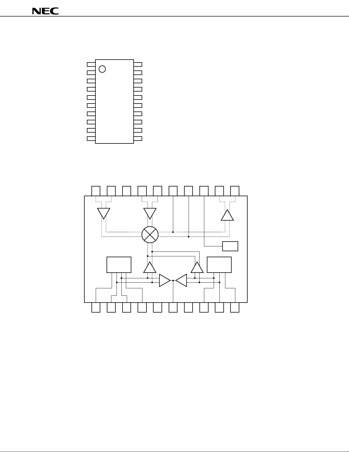
PIN CONFIGURATION (Top View)
1
2
3
4
5
6
7
8
9
10
INTERNAL BLOCK DIAGRAM
20
19
18
17
16
15
14
13
12
11
UOSC COLLECTOR (Tr.1)
1.
UOSC BASE (Tr.2)
2.
UOSC BASE (Tr.1)
3.
UOSC COLLECTOR (Tr.2)
4.
UB
5.
OSC OUTPUT
6.
GND
7.
VHF OSC BASE (Tr.1)
8.
VHF OSC BASE (Tr.2)
9.
10.
VHF OSC COLLECTOR (Tr.1)
11.
IF OUTPUT
12.
IF OUTPUT
13.
VCC
14.
MIXER OUTPUT1
15.
MIXER OUTPUT2
16.
VHF RF INPUT1
17.
VHF RF INPUT2
18.
GND
19.
UHF RF INPUT1
20.
UHF RF INPUT2
µ
PC2775GR/GS
20 19 18 17 16 15 14 13 12 11
U-RF
Pre Amp.
U-OSC U-OSC
12345678910
V-RF
Pre Amp.
MIX.
Buff.
U-PSC
Amp.
V-OSC
Buff.
V-PSC
Amp.
IF Amp.
REG.
V-OSC
2
Data Sheet P10194EJ3V0DS00

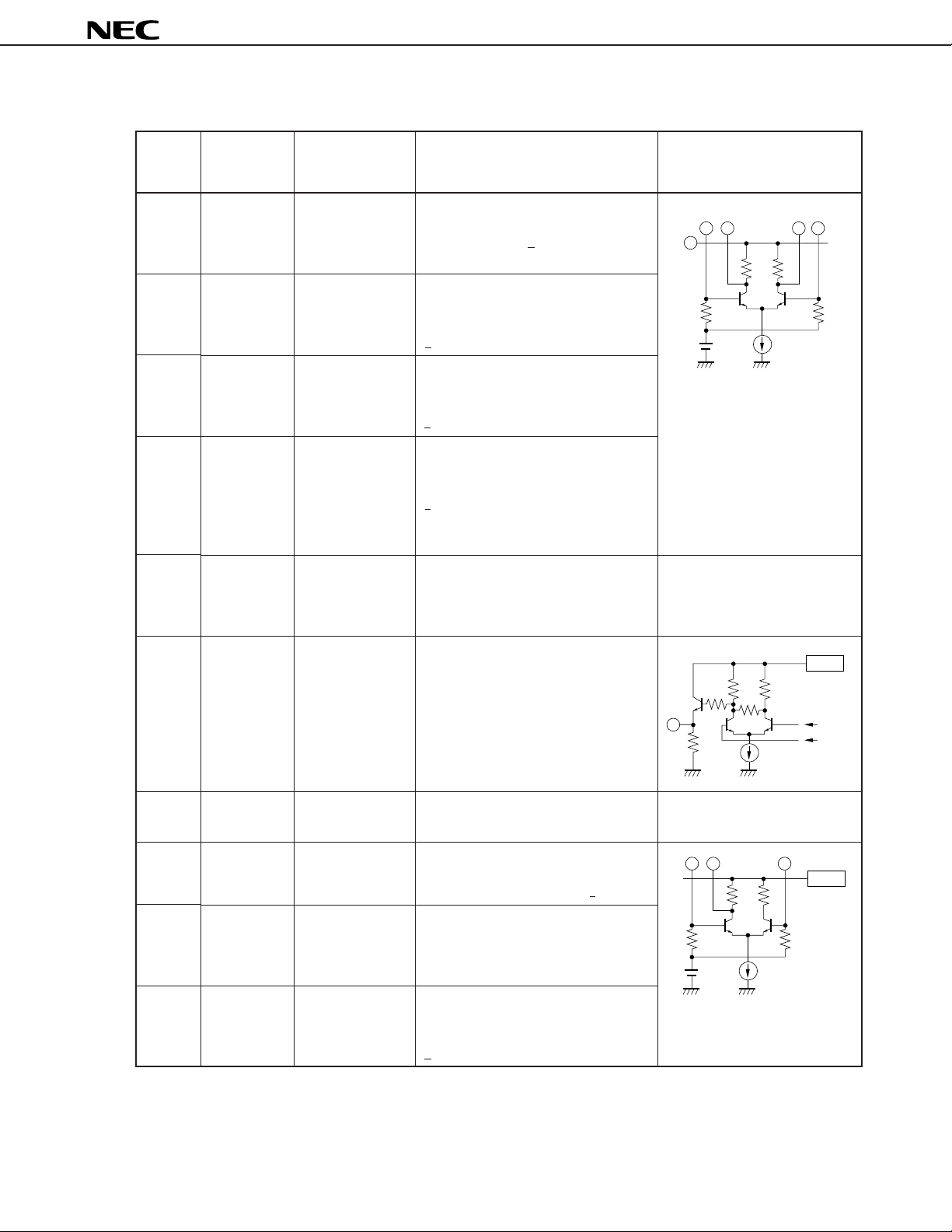
PIN EXPLANATION
Pin No.
1
2
3
4
5
6
Symbol
UOSC
collector
(Tr. 1)
UOSC
base (Tr. 2)
UOSC
base (Tr. 1)
UOSC
collector
(Tr. 2)
UB
OSC
output
Pin voltage TYP.
above: V mode (V)
below: U mode (U)
6.90
- - - - - - - - - - - - -
6.25
6.00
- - - - - - - - - - - - -
3.90
6.00
- - - - - - - - - - - - -
3.90
6.90
- - - - - - - - - - - - -
6.25
0.0
- - - - - - - - - - - - -
9.0
5.40
- - - - - - - - - - - - -
5.40
Collector pin of UHF oscillator.
Assemble LC resonator with 2 pin
through capacitor ~ 1 pF to oscillate
with active feedback Loop.
Base pin of UHF oscillator with
balance amplifier. Connected to LC
resonator through feedback capacitor
~ 300 pF.
Base pin of UHF oscillator with
balance amplifier. Connected to LC
resonator through feedback capacitor
~ 300 pF.
Collector pin of UHF oscillator with
balance amplifier. Assemble LC
resonator with 3 pin through capacitor
~ 1 pF to oscillate with active feedback
Loop. Double balanced oscillator with
transistor 1 and transistor 2.
Switching pin for VHF or UHF
operation.
UHF operation = 9.0 V
VHF operation = GND
UHF and VHF oscillator output pin.
In case of F/S tuner application,
connected PLL synthesizer IC’s input
pin.
µ
PC2775GR/GS
Equivalent circuitFunction and Explanation
5
6
2413
REG.
From
OSC
10
7
8
9
GND
VOSC
base (Tr. 1)
VOSC
base (Tr. 2)
VOSC
collector
(Tr. 1)
- - - - - - - - - - - - -
0.0
0.0
3.50
- - - - - - - - - - - - -
5.90
3.50
- - - - - - - - - - - - -
5.90
6.20
- - - - - - - - - - - - -
6.90
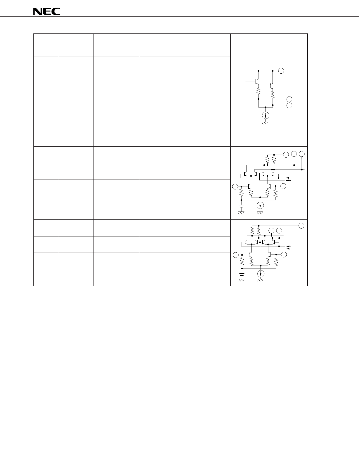
VHF and UHF oscillators’ GND pin.
Base pin of VHF oscillator with
balance amplifier.
Grounded through capacitor ~ 10 pF.
Base pin of VHF oscillator with
balance amplifier. Assemble LC
resonator with 10 pin to oscillate with
active feedback Loop.
Base pin of VHF oscillator with
balance amplifier. Connected to LC
resonator through feedback capacitor
~ 3 pF.
Data Sheet P10194EJ3V0DS00
10
8
9
REG.
3

11
11
12
13
12
Symbol
IF
output
Pin voltage TYP.
above: V mode (V)
below: U mode (U)
5.80
- - - - - - - - - - - - -
5.65
Function and Explanation
IF output pins of VHF-UHF band
functions.
Higher output power can be obtained
by connecting registor (ex. 470 Ω) to
the ground.
µ
PC2775GR/GS
Equivalent circuitPin No.
13
14
15
16
17
18
19
20
VCC
MIX
output 1
MIX
output 2
VRF
input
(bypass)
VRF input
GND
URF input
(bypass)
URF input
- - - - - - - - - - - - -
- - - - - - - - - - - - -
9.0
9.0
7.05
6.95
- - - - - - - - - - - - -
7.05
6.95
2.75
- - - - - - - - - - - - -
2.80
- - - - - - - - - - - - -
- - - - - - - - - - - - -
- - - - - - - - - - - - -
- - - - - - - - - - - - -
2.75
2.80
0
0
–
2.65
–
2.65
Power supply for VHF-UHF band
functions.
VHF and UHF MIX output pin.
These pins should be equipped with
tank circuit to adjust frequency.
VRF signal input pin from antenna.
Bypass pin for VHF MIX input.
Grounded through capacitor.
GND pin of MIX, IF amplifier and
regulator.
Bypass pin for UHF MIX input.
Grounded through capacitor.
URF signal input pin from antenna.
15
14
13
From
VHF
OSC
17
19
16
From
UHF
OSC
13
15
14
20
4
Data Sheet P10194EJ3V0DS00

µ
PC2775GR/GS
ABSOLUTE MAXIMUM RATINGS (TA = 25 °C)
µ
PC2775GR
PARAMETER SYMBOL RATING UNIT TEST CONDITION
Supply voltage 1 VCC 11.0 V
Supply voltage 2 UB 11.0 V
Power dissipation PD 500 mW TA = 75 °C
Operating temperature range TA –40 to +75 °C
Storage temperature range Tstg –60 to +150 °C
µ
PC2775GS
PARAMETER SYMBOL RATING UNIT TEST CONDITION
Supply voltage 1 VCC 11.0 V
Supply voltage 2 UB 11.0 V
Power dissipation PD 700 mW TA = 80 °C
Operating temperature range TA –40 to +80 °C
Storage temperature range Tstg –60 to +150 °C
Note 1
Note 1
Note 1 Mounted on 50 × 50 × 1.6 mm double copper epoxy glass board.
RECOMMENDED OPERATING RANGE
µ
PC2775GR
PARAMETER SYMBOL MIN. TYP. MAX. UNIT
Supply voltage 1 VCC 8.0 9.0 10.0 V
Supply voltage 2 UB 8.0 9.0 10.0 V
Operating temperature range TA –20 +25 +75 °C
µ
PC2775GS
PARAMETER SYMBOL MIN. TYP. MAX. UNIT
Supply voltage 1 VCC 8.0 9.0 10.0 V
Supply voltage 2 UB 8.0 9.0 10.0 V
Operating temperature range TA –20 +25 +80 °C
Data Sheet P10194EJ3V0DS00
5
 Loading...