NEC UPC2766GS-E1, UPC2766GS, UPC2766GR Datasheet

DATA SHEET
BIPOLAR ANALOG INTEGRATED CIRCUIT
µ
PC2766GR/GS
WIDE BAND IQ DEMODULATOR FOR DIGITAL VIDEO/DATA RECEIVER
DESCRIPTION
The µPC2766GR/GS is a Silicon monolithic IC designed for use as IQ demodulator in wide dynamic range
compressed video or spread spectrum receivers. This IC consists of a wide band RF amplifier, gain control amplifier,
dual balanced mixers (DBM), Lo buffers, and I & Q output buffer amplifiers.
µ
The package is 20 pin SSOP (shrink small outline package:
for high-density surface mount.
FEATURES
• Broadband operation RF & LO up to 1 000 MHz
IF (IQ) up to 200 MHz
• Wideband IQ phase and amplitude balance Amplitude balance ±0.3 dB (TYP.)
Phase balance ±0.3 degree (TYP.)
• AGC dynamic range 45 dB
• Low distortion; IM
• Supply Voltage 5 V
• Packaged in 20 pin SSOP or 20 pin SOP suitable for high-density surface mount
3 30 dBc
PC2766GR) or 20 pin SOP (µPC2766GS) suitable
ORDERING INFORMATION
PART NUMBER PACKAGE PACKAGE STYLE
µ
PC2766GR-E1
µ
PC2766GS-E1
The information in this document is subject to change without notice. Before using this document, please
confirm that this is the latest version.
Not all devices/types available in every country. Please check with local NEC representative for availability
and additional information.
20 pin plastic SSOP (225 mil)
20 pin plastic SOP (300 mil)
Caution electro-static sensitive device
Embossed tape 12 mm wide. 2.5 k/REEL
Pin 1 indicates pull-out direction of tape
Embossed tape 24 mm wide. 2.5 k/REEL
Pin 1 indicates pull-out direction of tape
Document No. P10193EJ4V0DS00 (4th edition)
Date Published October 1999 N CP(K)
Printed in Japan
The mark shows major revised points.
©
1995, 1999

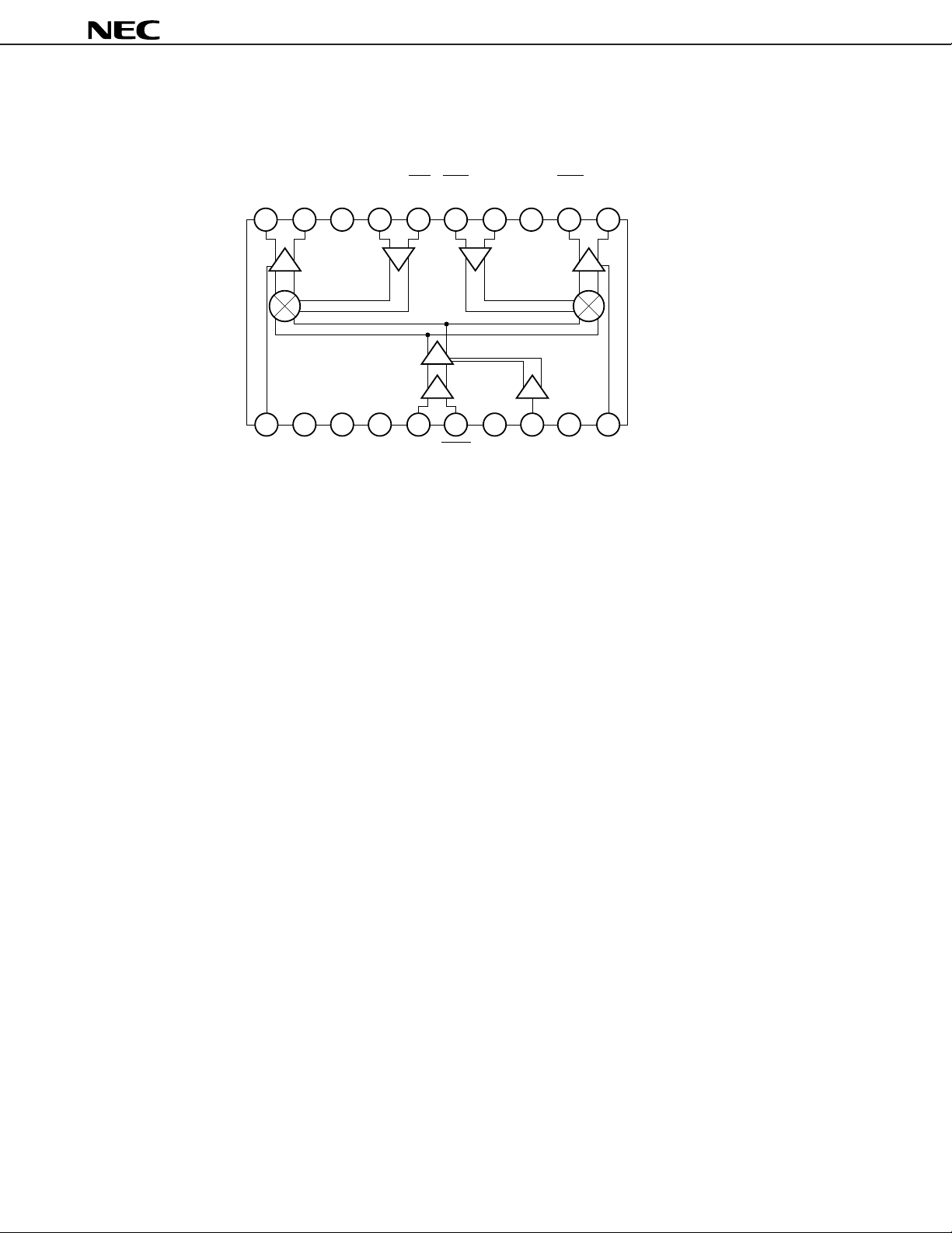
INTERNAL BLOCK DIAGRAM
µ
PC2766GR/GS
I out I out GND
20 19 18 17 16 15 14 13 12 11
I-IF Amp.
I-Lo.Buff.Amp I-Lo.Buff.Amp
I-MIX.
23
1
I trim Vcc
IF. I
Lo I Lo I Lo Q Lo Q GND
IF. I
RF AGC
RF Pre.Amp AGC cont.
4
VccRFGNDRFRF in RF in GNDRFVagc Vcc
678910
5
Q out Q out
IF. Q
I-IF Amp.
Q-MIX.
IF. Q
Q trim
2
Data Sheet P10193EJ4V0DS00

PIN FUNCTIONS
5
6
To next
block
V
CC
10
µ
PC2766GR/GS
PIN No. PIN NAME
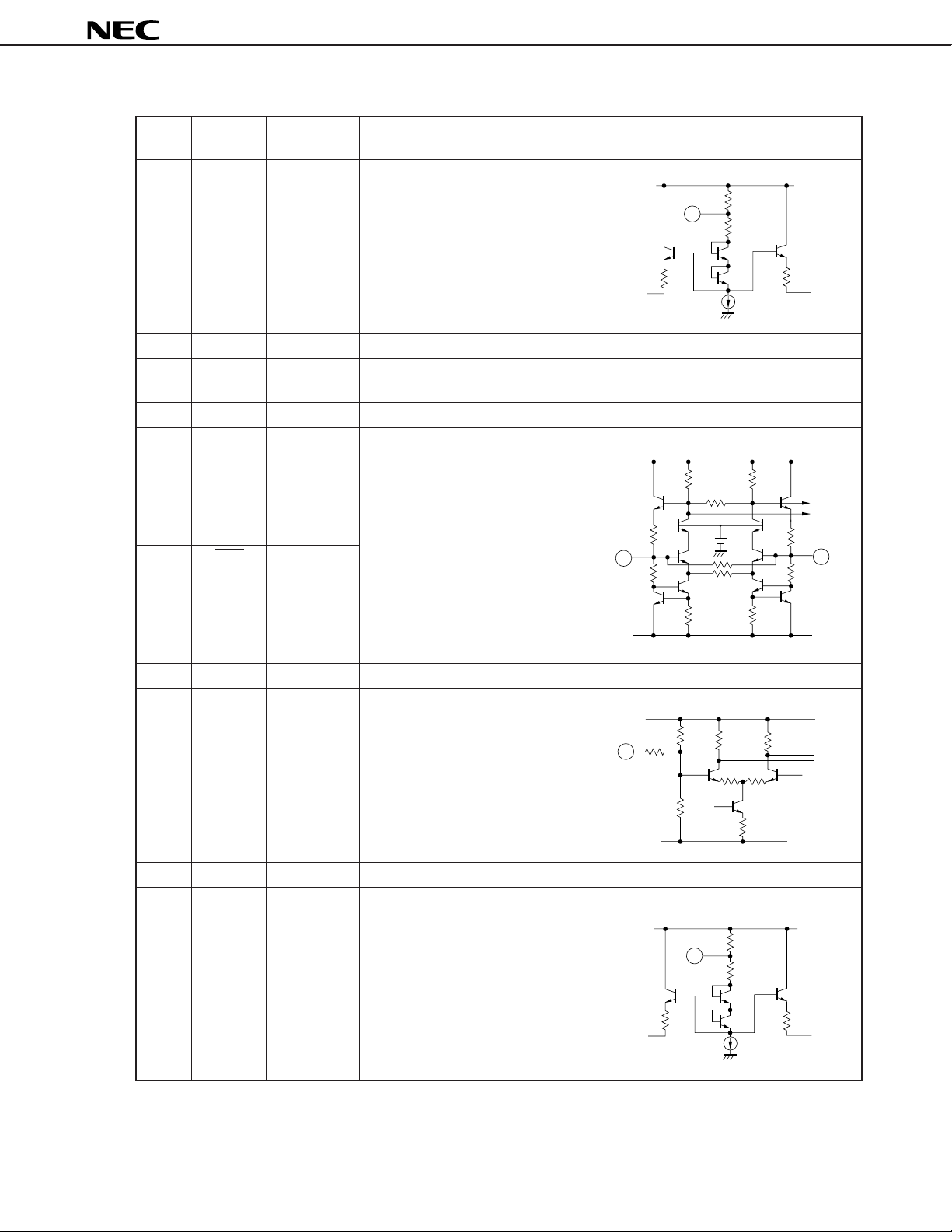
1 I Trim 4.2 Trimming pin for I-IF output.
2VCCIF I 5.0 Power supply pin for I-MIXER.
3VCCRF 5.0 Power supply pin for RF and AGC
4 GND RF 0.0 Ground pin of RF and AGC block.
5 RFin 2.6 RF input pin. In case of single input,
6 RFin 2.6
PIN VOLTAGE
TYP. (V)
FUNCTION AND EXPLANATION EQUIVALENT CIRCUIT
block.
6 pin should be grounded through
capacitor.
V
CC
1
7 GND RF 0.0 Ground pin of RF and AGC block.
8VAGC 0 to 5 Gain control pin.
CC
• VAGC = 0 V: Full gain
• VAGC = 5 V: Maximum reduction
9VCCIF Q 5.0 Power supply pin for Q-MIXER.
10 Q Trim 4.2 Trimming pin for Q-IF output.
8
V
Data Sheet P10193EJ4V0DS00
3

µ
PC2766GR/GS
PIN No. PIN NAME
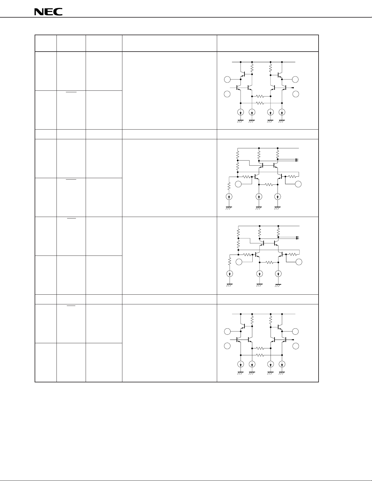
11 Qout 3.3 Q-IF output pin. 11 pin and 12 pin
12 Qout 3.3
13 GNDIF Q 0.0 Ground pin of Q-IF block.
14 Lo Q 2.2 Oscillator signal input pin of
15 Lo Q 2.2
PIN VOLTAGE
TYP. (V)
FUNCTION AND EXPLANATION EQUIVALENT CIRCUIT
are balance outputs.
Q-MIXER. In case of single input,
15 pin should be grounded through
capacitor.
12
V
CC
11
From
before
block
+
_
CC
V
1514
16 Lo I 2.2 Oscillator signal input pin of
I-MIXER. In case of single input,
16 pin should be grounded through
capacitor.
17 Lo I 2.2
18 GNDIF I 0.0 Ground pin of I-IF block.
19 Iout 3.3 I-IF output pin. 19 pin and 20 pin
are balance outputs.
20 Iout 3.3
19
CC
V
20
_
16
V
CC
From
before
block
17
+
4
Data Sheet P10193EJ4V0DS00

ABSOLUTE MAXIMUM RATINGS (TA = 25 °C)
µ
PC2766GR
PARAMETER SYMBOL RATING UNIT TEST CONDITIONS
Supply voltage VCC 6.0 V
Power dissipation PD 430 mW TA = 85 °C
Operating temperature range TA –40 to +85 °C
Storage temperature range Tstg –55 to +150 °C
µ
PC2766GS
PARAMETER SYMBOL RATING UNIT TEST CONDITIONS
Supply voltage VCC 6.0 V
Power dissipation PD 650 mW TA = 85 °C
Operating temperature range TA –40 to +85 °C
Storage temperature range Tstg –55 to +150 °C
µ
PC2766GR/GS
Note 1
Note 1
Note 1 Mounted on 50 × 50 × 1.6 mm double epoxy glass board.
RECOMMENDED OPERATING RANGE
µ
PC2766GR/GS
PARAMETER SYMBOL MAX. TYP. MIN. UNIT
Supply voltage VCC 4.5 5.0 5.5 V
Operating temperature range TA –40 +25 +85 °C
Data Sheet P10193EJ4V0DS00
5
 Loading...