

<R>
<R>
DATA SHEET
Solid State Relay
OCMOS FET
PS710A-1A,PS710AL-1A
6-PIN DIP, 0.1 Ω LOW ON-STATE RESISTANCE
1.8 A CONTINUOUS LOAD CURRENT
1-ch Optical Coupled MOS FET
DESCRIPTION
The PS710A-1A and PS710AL-1A are solid state relays containing GaAs LEDs on the light emitting side (input
side) and MOS FETs on the output side.
It is suitable for PLC, etc. because of its large continuous load current and low on-state resistance.
The PS710AL-1A has a surface mount type lead.
FEATURES
• Low on-state resistance (Ron = 0.1 Ω TYP.)
• Large continuous load current (I
• 1 channel type (1 a output)
• Low LED operating current (I
• Designed for AC/DC switching line changer
• Small package (6-pin DIP)
• Low offset voltage
• Ordering number of taping product: PS710AL-1A-E3, E4: 1 000 pcs/reel
• Pb-Free product
• Safety standards
• UL approved: File No. E72422
• BSI approved: No. 8245/8246
• CSA approved: No. CA 101391
APPLICATIONS
• Measurement equipment
• FA equipment
L = 1.8 A)
F = 2 mA)
−NEPOC Series−
The information in this document is subject to change without notice. Before using this document, please
confirm that this is the latest version.
Not all products and/or types are available in every country. Please check with an NEC Electronics
sales representative for availability and additional information.
Document No. PN10268EJ02V0DS (2nd edition)
Date Published July 2006 NS CP(K)
Printed in Japan
The revised points can be easily searched by copying an "<R>" in the PDF file and specifying it in the "Find what:" field.
The mark <R> shows major revised points.
1999, 2006

PACKAGE DIMENSIONS (in millimeters)
PS710A-1A,PS710AL-1A
PS710A-1A
4.15±0.3
3.3±0.3
0.5±0.1
1.34±0.1
0.25 M
3.5±0.3
9.25±0.5
2.54
PS710AL-1A
TOP VIEW
654
123
7.62
6.5±0.5
0 to 15˚
1. LED Anode
2. LED Cathode
3. NC
4. MOS FET Drain
5. MOS FET Source
6. MOS FET Drain
3.5±0.3
1.34±0.1
0.25 M
9.25±0.5
2.54
TOP VIEW
654
123
6.5±0.5
0.9±0.25
9.60±0.4
1. LED Anode
2. LED Cathode
3. NC
4. MOS FET Drain
5. MOS FET Source
6. MOS FET Drain
+0.10
–0.05
0.10
2
Data Sheet PN10268EJ02V0DS

PS710A-1A,PS710AL-1A
<R>
MARKING EXAMPLE
No. 1 pin
Mark
PS710A-1A
NL601
Rank Code
LN
6
01
Week Assembled
Year Assembled
(Last 1 Digit)
In-house Code
(L: Pb-Free)
Country Assembled
Type Number
Assembly Lot
Data Sheet PN10268EJ02V0DS
3
PS710A-1A,PS710AL-1A
<R>
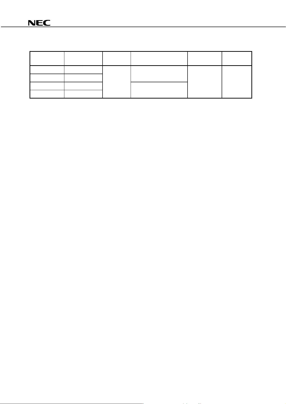
ORDERING INFORMATION
Part Number Order Number Solder Plating
Specification
PS710A-1A PS710A-1A-A Pb-Free Magazine case 50 pcs Standard products PS710A-1A
PS710AL-1A PS710AL-1A-A (UL, BSI, CSA
PS710AL-1A-E3 PS710AL-1A-E3-A Embossed Tape 1 000 pcs/reel approved)
PS710AL-1A-E4 PS710AL-1A-E4-A
*1 For the application of the Safety Standard, following part number should be used.
Packing Style Safety Standard
Approval
Application Part
Number
*1
4
Data Sheet PN10268EJ02V0DS

PS710A-1A,PS710AL-1A
ABSOLUTE MAXIMUM RATINGS (TA = 25°C, unless otherwise specified)
Parameter Symbol Ratings Unit
Diode Forward Current (DC) IF 50 mA
Reverse Voltage VR 5.0 V
Power Dissipation PD 50 mW
Peak Forward Current
MOS FET Break Down Voltage VL 60 V
Continuous Connection A IL 1.8 A
Load Current
*2
Connection C 3.6
Pulse Load Current
(AC/DC Connection)
Power Dissipation PD 560 mW
Isolation Voltage
*4
BV 1 500 Vr.m.s.
Total Power Dissipation PT 610 mW
Operating Ambient Temperature TA −40 to +85 °C
Storage Temperature Tstg −40 to +100 °C
*1 PW = 100
*2 Conditions: I
µ
s, Duty Cycle = 1%
F ≥ 2 mA. The following types of load connections are available.
*3 PW = 100 ms, 1 shot
*4 AC voltage for 1 minute at T
Pins 1-3 shorted together, 4-6 shorted together.
*1
IFP 1 A
Connection B 2.0
*3
Connection A VL (AC/DC)
Connection B
Connection C
A = 25°C, RH = 60% between input and output
ILP 3.6 A
1
25
3
1
2
6
I
L
4
6
5
L
L
I
L
+
V
L
(DC)
–
43
1
2
3
1
2
3
6
5
I
L
4
6
5
4
L
L
I
L
IL + I
I
L
L
–
V
L
(DC)
+
+
V
L
(DC)
–
Data Sheet PN10268EJ02V0DS
5
 Loading...