


<R>
DATA SHEET
PHOTOCOUPLER
PS2911-1
HIGH CTR, 4-PIN ULTRA SMALL PACKAGE
FLAT-LEAD PHOTOCOUPLER
DESCRIPTION
The PS2911-1 is an optically coupled isolator containing a GaAs light emitting diode and an NPN silicon
phototransistor in one package for high density mounting applications.
An ultra small flat-lead package has been provided which realizes a reduction in mounting area of about 30%
compared with the PS28xx series.
FEATURES
• Ultra small flat-lead package (4.6 (L) × 2.5 (W) × 2.1 (H) mm)
• High current transfer ratio (CTR = 200% TYP. @ I
• High isolation voltage (BV = 2 500 Vr.m.s.)
• Ordering number of taping product: PS2911-1-F3, F4: 3 500 pcs/reel
• Safety standards
• UL approved: File No. E72422
• BSI approved: No. 8657, 8658
• DIN EN60747-5-2 (VDE0884 Part2) approved (Option)
APPLICATIONS
• DC/DC converter
• Modem/PC card
F = 1 mA, VCE = 5 V)
−NEPOC Series−
The information in this document is subject to change without notice. Before using this document, please
confirm that this is the latest version.
Not all products and/or types are available in every country. Please check with an NEC Electronics
sales representative for availability and additional information.
Document No. PN10061EJ02V0DS (2nd edition)
Date Published May 2006 NS CP(K)
Printed in Japan
The revised points can be easily searched by copying an "<R>" in the PDF file and specifying it in the "Find what:" field.
The mark <R> shows major revised points.
2000, 2006

PACKAGE DIMENSIONS (UNIT: mm)
PS2911-1
<R>
2.5±0.3
4
N
12
2.1 MAX.
0.4±0.1
1.27
MARKING EXAMPLE
TOP VIEW
3
4.6±0.2
+0.1
–0.05
0.15
5.0±0.2
0.2±0.1
4.1 MIN.
43
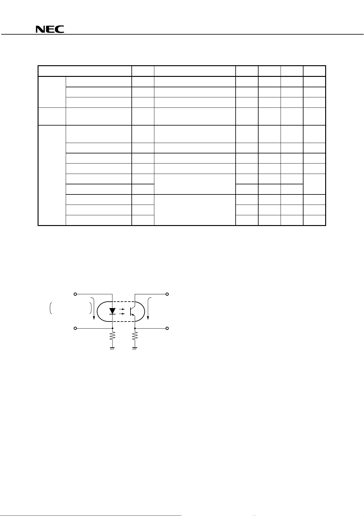
1. Anode
2. Cathode
3. Emitter
4. Collector
12
Last number of
11
N
601
No. 1 pin
mark
(Nicked
corner)
*1 Bar : Pb-Free
type No. : 11
*1
An initial of "NEC"
Assembly lot
01
6
Week assembled
Year assembled
PHOTOCOUPLER CONSTRUCTION
Parameter Unit (MIN.)
Air Distance 4 mm
Creepage Distance 4 mm
Isolation Distance 0.4 mm
2
Data Sheet PN10061EJ02V0DS

PS2911-1
<R>
ORDERING INFORMATION
Part Number Order Number
PS2911-1 PS2911-1-A Pb-Free 50 pcs (Tape 50 pcs cut) Standard products PS2911-1
PS2911-1-F3 PS2911-1-F3-A
PS2911-1-F4 PS2911-1-F4-A
PS2911-1-V PS2911-1-V-A
PS2911-1-V-F3 PS2911-1-V-F3-A
PS2911-1-V-F4 PS2911-1-V-F4-A
Solder Plating
Specification
Packing Style
Embossed Tape 3 500 pcs/reel (UL, BSI approved)
50 pcs (Tape 50 pcs cut) DIN EN60747-5-2
Embossed Tape 3 500 pcs/reel (VDE0884 Part2)
Approved (Option)
*1 For the application of the Safety Standard, following part number should be used.
Safety Standard
Approval
Application
Part Number
ABSOLUTE MAXIMUM RATINGS (TA = 25°C, unless otherwise specified)
Parameter Symbol Ratings Unit
Diode Forward Current IF 50 mA
Forward Current Derating
Power Dissipation PD 60 mW
Reverse Voltage VR 6 V
Transistor Collector to Emitter Voltage VCEO 40 V
Emitter to Collector Voltage VECO 5 V
Collector Current IC 40 mA
Power Dissipation Derating ∆PC/°C 1.2 mW/°C
Power Dissipation PC 120 mW
Isolation Voltage*2
Total Power Dissipation PT 160 mW
Operating Ambient Temperature TA −55 to +100 °C
Storage Temperature Tstg −55 to +150 °C
Peak Forward Current
*1
*1 PW = 100
µ
s, Duty Cycle = 1%
*2 AC voltage for 1 minute at T
Pins 1-2 shorted together, 3-4 shorted together.
∆
IF/°C 0.5 mA/°C
A = 25°C, RH = 60% between input and output
I
FP 0.5 A
BV 2 500 Vr.m.s.
*1
Data Sheet PN10061EJ02V0DS
3
PS2911-1
ELECTRICAL CHARACTERISTICS (TA = 25°C)
Parameter Symbol Conditions MIN. TYP. MAX. Unit
Diode Forward Voltage VF IF = 1 mA 0.9 1.1 1.3 V
Reverse Current IR VR = 5 V 5
Terminal Capacitance Ct V = 0 V, f = 1 MHz 15 pF
Transistor Collector to Emitter Dark
Current
Coupled Current Transfer Ratio
(I
C/IF)
*1
Collector Saturation Voltage VCE (sat) IF = 1 mA, IC = 0.2 mA 0.13 0.3 V
Isolation Resistance RI-O VI-O = 1 kVDC 1011
Isolation Capacitance CI-O V = 0 V, f = 1 MHz 0.4 pF
Rise Time
Fall Time
On Time
Storage Time
Off Time
*2
*2
*2
*2
*2
*1 CTR rank
N : 100 to 400 (%)
K : 200 to 400 (%)
L : 150 to 300 (%)
M : 100 to 200 (%)
*2 Test circuit for switching time
Pulse Input
ICEO IF = 0 mA, VCE = 40 V 100 nA
CTR I
F = 1 mA, VCE = 5 V 100 200 400 %
r VCC = 5 V, IC = 2 mA, RL = 100 Ω 5
t
f 10
t
t
on VCC = 5 V, IF = 1 mA, RL = 5 kΩ 40
s 10
t
t
off 120
V
CC
µ
A
Ω
µ
s
µ
s
µ
s
µ
s
PW = 100 s
Duty cycle = 1/10
In monitor
4
µ
I
F
50 Ω
I
C
V
RL = 100 Ω/5 kΩ
OUT
Data Sheet PN10061EJ02V0DS
 Loading...