

DATA SHEET
PHOTOCOUPLER
PS2841-4A,PS2841-4B
WORLD’S SMALLEST CLASS, FOUR CHANNELS
12-PIN ULTRA SHRINK SOP PHOTOCOUPLER
DESCRIPTION
The PS2841-4A and PS2841-4B are optically coupled isolators containing GaAs light emitting diodes and NPN
silicon phototransistors.
These products include four channels in a single package for high-density mounting applications.
The PS2841-4A and PS2841-4B are the world's smallest class of photocouplers and realize about 50% reduction in
mounting area compared with the PS280x and PS281x Series.
FEATURES
• Ultra small and thin package
(12-pin ultra shrink SOP, Pin pitch 0.8 mm, 4.4 (L) × 5.6 (W) × 2.5 (H))
• Common lead PS2841-4A: cathode, collector common
PS2841-4B: anode, collector common
• High current transfer ratio (CTR = 200% TYP. @ I
F = 1mA)
• High isolation voltage (BV = 1 500 Vr.m.s.)
• Pb-Free product
• Ordering number of tape product:
PS2841-4A-F3, F4: 2 500 pcs/reel
PS2841-4B-F3, F4: 2 500 pcs/reel
• Safety standards
• UL approved: File No. E72422
APPLICATIONS
• Programmable logic controllers (PLCs)
• Input and output for function automation
• Hybrid IC
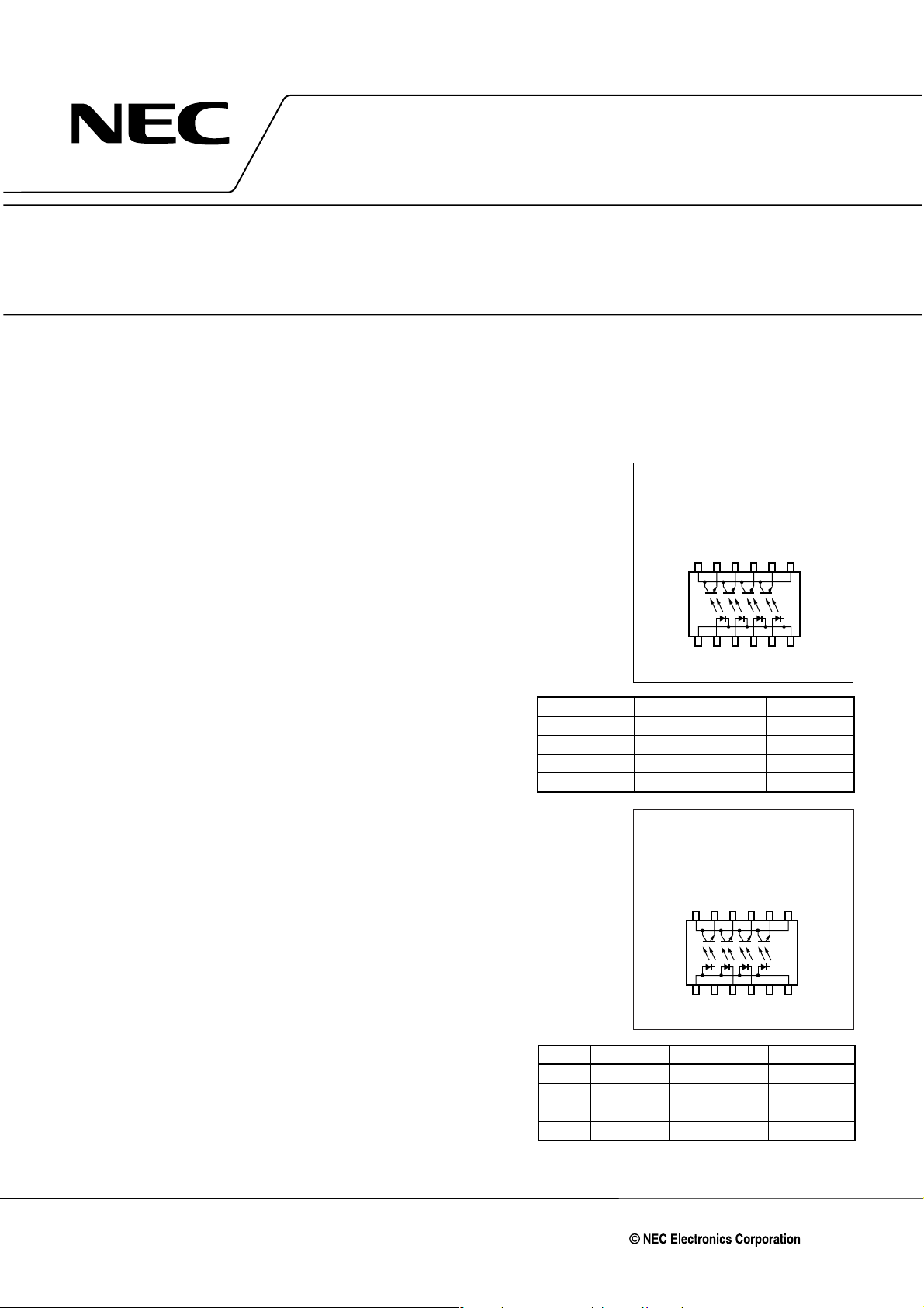
Channel
1 ch
2 ch
3 ch
4 ch
Anode
2
3
4
5
PIN CONNECTIONS
(Top View)
Cathode
1, 6 common
1, 6 common
1, 6 common
1, 6 common
PIN CONNECTIONS
−NEPOC Series−
PS2841-4A
12 11 10 9 8 7
123456
Emitter
11
7, 12 common
10
7, 12 common
9
7, 12 common
8
7, 12 common
(Top View)
PS2841-4B
12 11 10 9 8 7
Collector
The information in this document is subject to change without notice. Before using this document, please
confirm that this is the latest version.
Not all products and/or types are available in every country. Please check with an NEC Electronics
sales representative for availability and additional information.
Document No. PN10202EJ04V0DS (4th edition)
Date Published May 2006 NS CP(K)
Printed in Japan
The revised points can be easily searched by copying an "<R>" in the PDF file and specifying it in the "Find what:" field.
Channel
1 ch
2 ch
3 ch
4 ch
The mark <R> shows major revised points.
Anode
1, 6 common
1, 6 common
1, 6 common
1, 6 common
123456
Cathode
Emitter
2
11
3
10
4
5
9
8
Collector
7, 12 common
7, 12 common
7, 12 common
7, 12 common
2001, 2006
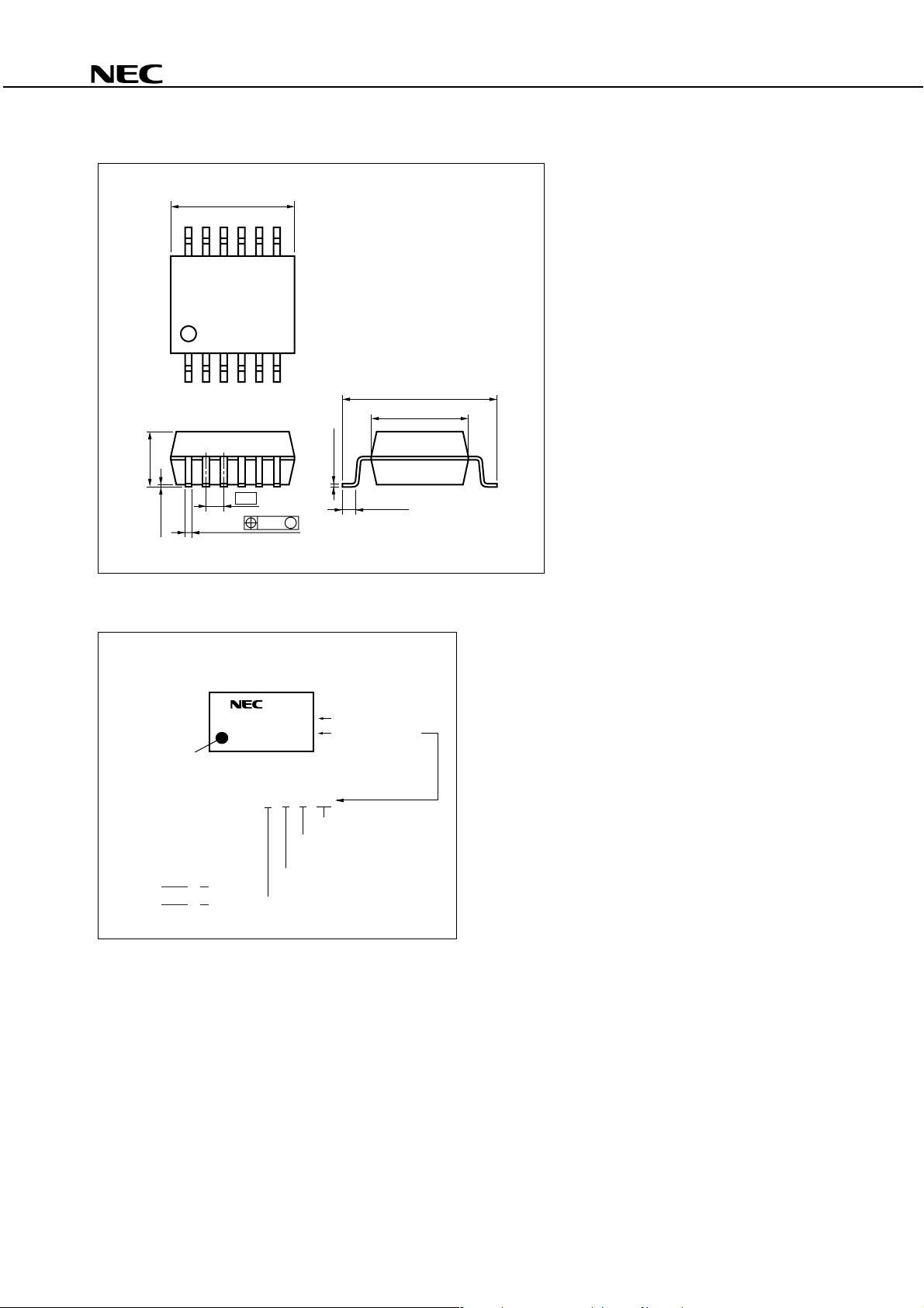
PACKAGE DIMENSIONS (UNIT: mm)
5.6±0.3
12
7
PS2841-4A,PS2841-4B
<R>
16
–0.2
+0.3
2.5
0.8
0.3±0.1
0.1±0.1
MARKING EXAMPLE
No. 1 pin
Mark
*1
Applicable type numbers
are underlined below
PS2841-4A
PS2841-4B
0.12
2841A
NL601
M
LN
6
01
Year Assembled
(Last 1 Digit)
In-house Code
(L: Pb-Free)
Rank Code
7.0±0.3
–0.05
+0.10
0.15
0.5±0.3
Type Number
Assembly Lot
Week Assembled
4.4
*1
2
Data Sheet PN10202EJ04V0DS

PS2841-4A,PS2841-4B
<R>
ORDERING INFORMATION
Part Number Order Number Solder Plating
Specification
PS2841-4A-F3 PS2841-4A-F3-A Pb-Free Embossed Tape 2 500 pcs/reel Standard products PS2841-4A
PS2841-4A-F4 PS2841-4A-F4-A (UL Approved)
PS2841-4B-F3 PS2841-4B-F3-A PS2841-4B
PS2841-4B-F4 PS2841-4B-F4-A
Packing Style Safety Standard
Approval
Application Part
Number
*1 For the application of the Safety Standard, following part number should be used.
ABSOLUTE MAXIMUM RATINGS (TA = 25°C, unless otherwise specified)
Parameter Symbol Ratings Unit
Diode Forward Current (DC) IF 20 mA/ch
Reverse Voltage VR 6 V
Power Dissipation Derating ∆ IF /°C 0.2 mA /°C
Peak Forward Current
Transistor Collector to Emitter Voltage VCEO 70 V
Emitter to Collector Voltage VECO 5 V
Collector Current IC 20 mA/ch
Power Dissipation Derating ∆PC/°C 0.4 mW/°C
Power Dissipation PC 40 mW/ch
Isolation Voltage
Operating Ambient Temperature TA –40 to +100 °C
Storage Temperature Tstg –55 to +125 °C
*2
BV 1 500 Vr.m.s.
µ
*1 PW = 100
s, Duty Cycle = 1%
*2 AC voltage for 1 minute at T
Pins 1-6 shorted together, 7-12 shorted together.
*1
IFP 0.5 A/ch
A = 25°C, RH = 60% between input and output.
*1
Data Sheet PN10202EJ04V0DS
3

PS2841-4A,PS2841-4B
ELECTRICAL CHARACTERISTICS (TA = 25°C)
Parameter Symbol Conditions MIN. TYP. MAX. Unit
Diode Forward Voltage VF IF = 1 mA 0.9 1.1 1.2 V
Reverse Current IR VR = 5 V 10
Terminal Capacitance Ct V = 0 V, f = 1 MHz 15 pF
Transistor Collector to Emitter Current ICEO IF = 0 mA, VCE = 24 V 100 nA
Coupled Current Transfer Ratio (IC/IF) CTR IF = 1 mA, VCE = 0.4 V 100 200 400 %
Optical Leakage Current
(1 to 2-ch, 2 to 3-ch, 3 to 4-ch)
Collector Saturation Voltage VCE (sat) IF = 1 mA, IC = 0.2 mA 0.13 0.3 V
Isolation Resistance RI-O VI-O = 1 kVDC 1011
Isolation Capacitance CI-O V = 0 V, f = 1 MHz 0.4 pF
Turn-on Time
Turn-off Time
*2
ton VCC = 5 V, IF = 1 mA, RL = 5 kΩ 20 µs
*2
toff 110
*1 The optically induced leakage current is current which can be measured at transistor if LED = ”ON” and LED =
”OFF”.
LED of channel 1 is switched to ”ON”.
At Tr-output of channel 2 a voltage is applied and one can measure a current between emitter and collector.
This is leakage current (at I
Measurement circuits for optical leakage current
E.g. : In the case of 1 to 2-ch (PS2841-4A)
I
F
1
*1
F = 5 mA, VCEO = 24 V).
IL IF = 5 mA, VCE = 24 V 100 nA
12
µ
A
Ω
2
3
4
5
6
*2 Test circuit for switching time
Pulse Input
PW = 100 s
Duty cycle = 1/10
In monitor
µ
IF
50 Ω
11
10
9
8
7
A
I
L
RL = 5 kΩ
VCC
VOUT
4
Data Sheet PN10202EJ04V0DS
 Loading...