

Page 1

µ
User’s Manual
78K0/Kx2
8-Bit Single-Chip Microcontrollers
Flash Memory Self Programming
µ
PD78F0500
µ
PD78F0501
µ
PD78F0502
µ
PD78F0503
µ
PD78F0503D
µ
PD78F0511
µ
PD78F0512
µ
PD78F0513
µ
PD78F0513D
µ
PD78F0514
µ
PD78F0515
µ
PD78F0515D
µ
PD78F0521
µ
PD78F0522
µ
PD78F0523
µ
PD78F0524
µ
PD78F0525
µ
PD78F0526
µ
PD78F0527
µ
PD78F0527D
µ
PD78F0531
µ
PD78F0532
µ
PD78F0533
µ
PD78F0534
µ
PD78F0535
µ
PD78F0536
µ
PD78F0537
µ
PD78F0544
µ
PD78F0545
µ
PD78F0546
µ
PD78F0547
µ
PD78F0547D
PD78F0537D
Document No. U17516EJ1V0UM00 (1st edition)
Date Published August 2005 N CP(K)
2005
Printed in Japan
Page 2

[MEMO]
2 User’s Manual U17516EJ1V0UM
Page 3
NOTES FOR CMOS DEVICES
1
VOLTAGE APPLICATION WAVEFORM AT INPUT PIN
Waveform distor tion due to input noise or a reflected wave may cause malfunction. If the input of the
CMOS device stays in the area between V
malfunction. Take care to prevent chattering noise from entering the device when the input level is fixed,
and also in the transition period when the input level passes through the area between V
V
IH
(MIN).
HANDLING OF UNUSED INPUT PINS
2
Unconnected CMOS device inputs can be cause of malfunction. If an input pin is unconnected, it is
possible that an internal input level may be generated due to noise, etc., causing malfunction. CMOS
devices behave differently than Bipolar or NMOS devices. Input levels of CMOS devices must be fixed
high or low by using pull-up or pull-down circuitry. Each unused pin should be connected to V
via a resistor if there is a possibility that it will be an output pin. All handling related to unused pins must
be judged separately for each device and according to related specifications governing the device.
3
PRECAUTION AGAINST ESD
A strong electric field, when exposed to a MOS device, can cause destruction of the gate oxide and
ultimately degrade the device operation. Steps must be taken to stop generation of static electricity as
much as possible, and quickly dissipate it when it has occurred. Environmental control must be
adequate. When it is dry, a humidifier should be used. It is recommended to avoid using insulators that
easily build up static electricity. Semiconductor devices must be stored and transported in an anti-static
container, static shielding bag or conductive material. All test and measurement tools including work
benches and floors should be grounded. The operator should be grounded using a wrist strap.
Semiconductor devices must not be touched with bare hands. Similar precautions need to be taken for
PW boards with mounted semiconductor devices.
IL
(MAX) and VIH (MIN) due to noise, etc., the device may
IL
(MAX) and
DD
or GND
4
STATUS BEFORE INITIALIZATION
Power-on does not necessarily define the initial status of a MOS device. Immediately after the power
source is turned ON, devices with reset functions have not yet been initialized. Hence, power-on does
not guarantee output pin levels, I/O settings or contents of registers. A device is not initialized until the
reset signal is received. A reset operation must be executed immediately after power-on for devices
with reset functions.
5
POWER ON/OFF SEQUENCE
In the case of a device that uses different power supplies for the internal operation and external
interface, as a rule, switch on the external power supply after switching on the internal power supply.
When switching the power supply off, as a rule, switch off the external power supply and then the
internal power supply. Use of the reverse power on/off sequences may result in the application of an
overvoltage to the internal elements of the device, causing malfunction and degradation of internal
elements due to the passage of an abnormal current.
The correct power on/off sequence must be judged separately for each device and according to related
specifications governing the device.
6
INPUT OF SIGNAL DURING POWER OFF STATE
Do not input signals or an I/O pull-up power supply while the device is not powered. The current
injection that results from input of such a signal or I/O pull-up power supply may cause malfunction and
the abnormal current that passes in the device at this time may cause degradation of internal elements.
Input of signals during the power off state must be judged separately for each device and according to
related specifications governing the device.
User’s Manual U17516EJ1V0UM 3
Page 4

•
The information in this document is current as of July, 2005. The information is subject to change
without notice. For actual design-in, refer to the latest publications of NEC Electronics data sheets or
data books, etc., for the most up-to-date specifications of NEC Electronics products. Not all
products and/or types are available in every country. Please check with an NEC Electronics sales
representative for availability and additional information.
No part of this document may be copied or reproduced in any form or by any means without the prior
•
written consent of NEC Electronics. NEC Electronics assumes no responsibility for any errors that may
appear in this document.
•
NEC Electronics does not assume any liability for infringement of patents, copyrights or other intellectual
property rights of third parties by or arising from the use of NEC Electronics products listed in this document
or any other liability arising from the use of such products. No license, express, implied or otherwise, is
granted under any patents, copyrights or other intellectual property rights of NEC Electronics or others.
Descriptions of circuits, software and other related information in this document are provided for illustrative
•
purposes in semiconductor product operation and application examples. The incorporation of these
circuits, software and information in the design of a customer's equipment shall be done under the full
responsibility of the customer. NEC Electronics assumes no responsibility for any losses incurred by
customers or third parties arising from the use of these circuits, software and information.
•
While NEC Electronics endeavors to enhance the quality, reliability and safety of NEC Electronics products,
customers agree and acknowledge that the possibility of defects thereof cannot be eliminated entirely. To
minimize risks of damage to property or injury (including death) to persons arising from defects in NEC
Electronics products, customers must incorporate sufficient safety measures in their design, such as
redundancy, fire-containment and anti-failure features.
•
NEC Electronics products are classified into the following three quality grades: "Standard", "Special" and
"Specific".
The "Specific" quality grade applies only to NEC Electronics products developed based on a customerdesignated "quality assurance program" for a specific application. The recommended applications of an NEC
Electronics product depend on its quality grade, as indicated below. Customers must check the quality grade of
each NEC Electronics product before using it in a particular application.
"Standard": Computers, office equipment, communications equipment, test and measurement equipment, audio
and visual equipment, home electronic appliances, machine tools, personal electronic equipment
and industrial robots.
"Special": Transportation equipment (automobiles, trains, ships, etc.), traffic control systems, anti-disaster
systems, anti-crime systems, safety equipment and medical equipment (not specifically designed
for life support).
"Specific": Aircraft, aerospace equipment, submersible repeaters, nuclear reactor control systems, life
support systems and medical equipment for life support, etc.
The quality grade of NEC Electronics products is "Standard" unless otherwise expressly specified in NEC
Electronics data sheets or data books, etc. If customers wish to use NEC Electronics products in applications
not intended by NEC Electronics, they must contact an NEC Electronics sales representative in advance to
determine NEC Electronics' willingness to support a given application.
(Note)
(1) "NEC Electronics" as used in this statement means NEC Electronics Corporation and also includes its
majority-owned subsidiaries.
(2) "NEC Electronics products" means any product developed or manufactured by or for NEC Electronics (as
defined above).
M8E 02. 11-1
4 User’s Manual U17516EJ1V0UM
Page 5

Regional Information
Some information contained in this document may vary from country to country. Before using any NEC
Electronics product in your application, pIease contact the NEC Electronics office in your country to
obtain a list of authorized representatives and distributors. They will verify:
•
Device availability
•
Ordering information
•
Product release schedule
•
Availability of related technical literature
•
Development environment specifications (for example, specifications for third-party tools and
components, host computers, power plugs, AC supply voltages, and so forth)
•
Network requirements
In addition, trademarks, registered trademarks, export restrictions, and other legal issues may also vary
from country to country.
[GLOBAL SUPPORT]
http://www.necel.com/en/support/support.html
NEC Electronics America, Inc. (U.S.)
Santa Clara, California
Tel: 408-588-6000
800-366-9782
N
EC Electronics (Europe) GmbH
Duesseldorf, Germany
Tel: 0211-65030
•
Sucursal en España
Madrid, Spain
Tel: 091-504 27 87
•
Succursale Française
Vélizy-Villacoublay, France
Tel: 01-30-67 58 00
•
Filiale Italiana
Milano, Italy
Tel: 02-66 75 41
•
Branch The Netherlands
Eindhoven, The Netherlands
Tel: 040-265 40 10
•
Tyskland Filial
Taeby, Sweden
Tel: 08-63 87 200
•
United Kingdom Branch
Milton Keynes, UK
Tel: 01908-691-133
NEC Electronics Hong Kong Ltd.
Hong Kong
Tel: 2886-9318
NEC Electronics Hong Kong Ltd.
Seoul Branch
Seoul, Korea
Tel: 02-558-3737
NEC Electronics Shanghai Ltd.
Shanghai, P.R. China
Tel: 021-5888-5400
NEC Electronics Taiwan Ltd.
Taipei, Taiwan
Tel: 02-2719-2377
NEC Electronics Singapore Pte. Ltd.
Novena Square, Singapore
Tel: 6253-8311
J05.6
User’s Manual U17516EJ1V0UM 5
Page 6

INTRODUCTION
Readers This manual is intended for users who wish to understand the functions of the flash
memory versions of the 78K0/Kx2 and design application systems using these
microcontrollers.
Purpose This manual is intended to give users an understanding of the usage of the flash
memory self programming sample library which is used when rewriting the 78K0/Kx2
flash memory.
Organization This manual can be generally divided into the following sections.
• Description of flash environment
• Description of flash memory self programming sample library
How to Read This Manual It is assumed that the readers of this manual have general knowled ge in the fields of
electrical engineering, logic circuits, and microcontrollers.
To check the hardware functions of the 78K0/Kx2
→ Refer to the user’s manual of each 78k0/Kx2 product.
Conventions Data significance: Higher digits on the left and lower digits on the right
Active low representation: xxx (overscore over pin or signal name)
Note: Footnote for item marked with Note in the text
Caution: Information requiring particular attention
Remark: Supplementary information
Numerical representation: Binary … xxxx or xxxxB
Decimal … xxxx
Hexadecimal … xxxxH
6 User’s Manual U17516EJ1V0UM
Page 7

Terminology The following describes the meanings of certain terms used in this manual.
• Self programming
Self programming operations are flash memory write operations th at are performed
by user programs.
• Flash memory self programming sample library
This is the library that is provided by the 78K0/Kx2 for flash memory manipulation.
• Flash environment
This is the environment that supports flash memory manipulations. It has
restrictions that differ from those applied to ordinary program execution.
• Block number
Block numbers indicate blocks in flash memory. They are used as units during
manipulations such as erasures and blank checks.
• Boot cluster
This is the area that is used for boot swapping. Boot cluster 0 and boot cluster 1
are provided and the cluster to be booted can be selected.
• Entry RAM
This is the area in RAM that is used by the flash memory self programmi ng sample
library. The user program reserves this area and specifies the start address of the
specific area to be used when the library is called.
• Internal verification
After writing to flash memory, signal levels are checked internally to confirm correct
reading of data. When an internal verification error occurs, the corresponding
device is judged as faulty.
User’s Manual U17516EJ1V0UM 7
Page 8

CONTENTS
CHAPTER 1 GENERAL........................................................................................................................... 11
1.1 Overview..................................................................................................................................... 11
1.2 Calling Self Programming Sample Library ............................................................................. 11
1.3 Bank Number and Block Number ............................................................................................14
1.4 Processing Time and Acknowledging Interrupt.....................................................................17
CHAPTER 2 PROGRAMMING ENVIRONMENT .................................................................................... 20
2.1 Hardware Environment.............................................................................................................. 20
2.2 Software Environment...............................................................................................................21
2.2.1 Entry RAM........................................................................................................................................... 22
2.2.2 Stack and data buffer...........................................................................................................................23
CHAPTER 3 INTERRUPT SERVICING DURING SELF PROGRAMMING............................................ 24
3.1 Overview..................................................................................................................................... 24
3.2 Interrupt Response Time........................................................................................................... 27
3.3 Description Example................................................................................................................. 29
3.4 Cautions ..................................................................................................................................... 31
CHAPTER 4 BOOT SWAP FUNCTION...................................................................................................32
CHAPTER 5 SELF PROGRAMMING SAMPLE LIBRARY..................................................................... 39
5.1 Type of Self Programming Sample Library............................................................................. 39
5.2 Explanation of Self Programming Sample Library.................................................................40
self programming start library .....................................................................................................................41
initialize library ............................................................................................................................................43
mode check library...................................................................................................................................... 45
block blank check library .............................................................................................................................47
block erase library....................................................................................................................................... 51
word write library......................................................................................................................................... 55
block verify library....................................................................................................................................... 60
self programming end library ......................................................................................................................64
get information library .................................................................................................................................66
set information library.................................................................................................................................. 72
EEPROM write library.................................................................................................................................76
CHAPTER 6 DETAILS OF SELF PROGRAMMING CONTROL.............................................................81
6.1 Registers That Control Self Programming.............................................................................. 81
6.1.1 Flash programming mode control register (FLPMC)............................................................................ 81
6.1.2 Flash protect command register (PFCMD)..........................................................................................83
6.1.3 Flash status register (PFS)..................................................................................................................84
6.1.4 Self programming control parameters..................................................................................................85
APPENDIX A SAMPLE PROGRAM........................................................................................................90
A.1 User Program.............................................................................................................................90
A.2 Self Programming Library (Normal Model)...........................................................................103
A.3 Self Programming Library (Static Model)..............................................................................118
A.4 Boot Swap ................................................................................................................................132
A.5 Compiling the Flash Self Programming Sample Library and Sample Program................137
APPENDIX B INDEX..............................................................................................................................138
8
User’s Manual U17516EJ1V0UM
Page 9

LIST OF FIGURES
Figure 1-1 Flow of Self Programming (rewriting contents of flash memory).......................................................12
Figure 1-2 Block Numbers and Boot Clusters (flash memory of up to 60 KB) ...................................................15
Figure 1-3 Block Numbers and Boot Clusters (flash memory of 96 KB or more)...............................................16
Figure 2-1 FLMD0 Voltage Generator................................................................................................................20
Figure 2-2 Allocation Range of Entry RAM........................................................................................................22
Figure 2-3 Allocatable Range for Stack Pointer and Data Buffer .......................................................................23
Figure 3-1 Flow of Processing in Case of Interrupt............................................................................................ 25
Figure 4-1 Flow of Boot Swapping.....................................................................................................................33
Figure 5-1 Flow of Self Programming Start Library............................................................................................ 42
Figure 5-2 Flow of Initialize Library....................................................................................................................44
Figure 5-3 Flow of Mode Check Library.............................................................................................................46
Figure 5-4 Flow of Block Blank Check Library................................................................................................... 50
Figure 5-5 Flow of Block Erase Library..............................................................................................................54
Figure 5-6 Flow of Word Write Library ...............................................................................................................59
Figure 5-7 Flow of Block V e rify Library............................................................................................................... 63
Figure 5-8 Flow of Self Programming End Library.............................................................................................65
Figure 5-9 Flow of Get Information Library ........................................................................................................71
Figure 5-10 Flow of Set Information Library.........................................................................................................75
Figure 5-11 Flow of EEPROM Write Library........................................................................................................ 80
Figure 6-1 Self Programming Operation Mode and Memory Map (µPD78F0545).............................................82
Figure 6-2 Write Protection................................................................................................................................83
User’s Manual U17516EJ1V0UM
9
Page 10

LIST OF TABLES
Table 1-1 Processing Time and Acknowledging Interrupt (with internal high-speed oscillator).........................18
Table 1-2 Processing Time and Acknowledging Interrupt (with external system clock used) ...........................19
Table 2-1 Software Resources .........................................................................................................................21
Table 3-1 Resume Processing Stopped by Interrupt ........................................................................................26
Table 3-2 Interrupt Response Time (with Internal High-Speed Oscillator)........................................................27
Table 3-3 Interrupt Response Time (with External System Clock)....................................................................28
Table 5-1 Self programming sample library List................................................................................................39
Table 6-1 Register Bank 3 Parameter List........................................................................................................86
Table 6-2 Entry RAM Parameter List................................................................................................................87
Table 6-3 Data Buffer Parameter List................................................................................................................88
Table 6-4 Detailed Flash Information for Get Information Function...................................................................89
10
User’s Manual U17516EJ1V0UM
Page 11

CHAPTER 1 GENERAL
1.1 Overview
The self programming sample library is firmware provided on the 78K0/Kx2, and is software which is used to rewrite
data in the flash memory.
By calling the self programming sample library from a user program, the contents of the flash memor y can be
rewritten and, consequently, the period for software development can be substantially shortened.
Cautions 1. Because the self programming sample library rewrites the contents of the flash memory by
using the CPU, registers, and RAM of the 78K0/Kx2, a user program cannot be executed while
processing of the self programming sample library is being executed.
2. The self programming sample library uses the CPU (register bank 3) and a work area (100
bytes of entry RAM). Therefore, the user must save the data necessary for the user program
in that area immediately before calling the self programming sample library.
1.2 Calling Self Programming Sample Library
The self programming sample library can be called by a user program in C or an assembly language.
If the -SM option (that uses an object as a static model) is specified when a file written in C is complie d, use (link)
the library for static models. If the -SM option is not specified, link the library for normal models.
If the file is written in an assembly language, use (link) the library for static models.
User’s Manual U17516EJ1V0UM
11
Page 12
CHAPTER 1 GENERAL
k
The following flowchart illustrates how to rewrite the contents of the flash memory by using the self programming
sample library.
Figure 1-1. Flow of Self Programming (rewriting contents of flash memory)
Starting self programming
<1>
<2>
<3>
<4>
<5>
<6>
<8>
FLMD0 pin: Low → High
FlashStart
Setting operating environment
FlashEnv
CheckFLMD
Normal
completion?
Yes
FlashBlockBlankChec
Erased?
Yes
<7>
FlashWordWrite
No
No
FlashBlockErase
Normal
completion?
Yes
No
No
No
<9>
<10>
<11>
Normal
completion?
Yes
FlashBlockVerify
Normal
completion?
Yes
FlashEnd
FLMD0 pin: High → Low
End of self programming
12
User’s Manual U17516EJ1V0UM
Page 13

CHAPTER 1 GENERAL
<1> Preprocessing (setting of hardware environment)
As preprocessing, make the FLMD0 pin high (refer to 2.1 Hardware Environment).
<2> Preprocessing (declaring start of self programming)
As preprocessing, call the self programming start library FlashStart to declare the start of self programming.
<3> Preprocessing (setting of software environment)
As preprocessing, save register bank 3 and specify a work area (refer to 2.2 Software Environment).
<4> Preprocessing (initializing entry RAM)
As preprocessing, call the initialize library FlashEnv to initialize the entry RAM.
<5> Preprocessing (checking voltage level)
As preprocessing, call the mode check library CheckFLMD and check the voltage level.
<6> Checking erasing of specified block (1 KB)
Call the block blank check library FlashBlockBlankCheck to check if the specified block (1 KB) has been erased.
<7> Erasing specified block (1 KB)
Call the block erase library FlashBlockErase to erase a specified block (1 KB).
<8> Writing data of 1 to 64 words to specified addresses
Call the word write library FlashWordWrite to write data of 1 to 64 words to specified addresses.
<9> Verifying specified block (1 KB) (internal verification)
Call the block verify library FlashBlockVerify to verify a specified block (1 KB) (internal verification).
<10> Post-processing (declaring end of self programming)
As post-processing, call the self programming end library FlashEnd to declare the end of self programming.
<11> Post-processing (setting of hardware environment)
As post-processing, return the level of the FLMD0 pin to the low level.
User’s Manual U17516EJ1V0UM
13
Page 14

CHAPTER 1 GENERAL
1.3 Bank Number and Block Number
Products in the 78K0/Kx2 Series having flash memor y of up to 60 KB have their flash memory divided into 1 KB
blocks. Erasing, blank checking, and verification (internal verification) for self programming are performed in these
block units. To call the self programming sample library, a block number is specified.
Addresses 0000H to 0FFFH and 1000H to 1FFFH of the 78K0/Kx2 are allocated for boot clusters. A boot cluster is
an area that is used to prevent the vector table data and basic functions of the program from being destroyed, and to
prevent the user program from being unable to start due to a power failure or because the device was reset while an
area including a vector area was being rewritten. For details on the boot cluster, refer to CHAPTER 4 BOOT SWAP
FUNCTION.
Figure 1-2 shows the block numbers and boot clusters of a flash memory of up to 60 KB.
78K0/Kx2 products having flash memory of more than 96 KB have banks in an area that is larger than 32 KB. For
these products, not only a block number but also a bank number must be specified to call the self programming sample
library when performing erasing, blank checking, or verification (internal verification) in the are a that is larger than 32
KB during self programming.
Figure 1-3 shows the block numbers and boot clusters of a flash memory of more than 96 KB.
14
User’s Manual U17516EJ1V0UM
Page 15
CHAPTER 1 GENERAL
000
Figure 1-2. Block Numbers and Boot Clusters (flash memory of up to 60 KB)
8000H
7C00H
7800H
7400H
7000H
6C00H
6800H
6400H
6000H
5C00H
5800H
5400H
5000H
4C00H
4800H
4400H
4000H
3C00H
3800H
3400H
3000H
2C00H
2800H
2400H
2000H
1C00H
1800H
1400H
1000H
0C00H
0800H
0400H
0000H
Block 31
Block 30
Block 29
Block 28
Block 27
Block 26
Block 25
Block 24
Block 23
Block 22
Block 21
Block 20
Block 19
Block 18
Block 17
Block 16
Block 15
Block 14
Block 13
Block 12
Block 11
Block 10
Block 9
Block 8
Block 7
Block 6
Block 5
Block 4
Block 3
Block 2
Block 1
Block 0
F800H
Internal expansion RAM
H
F
EC00H
E800H
E400H
E000H
DC00H
D800H
D400H
D000H
CC00H
C800H
C400H
C000H
BC00H
B800H
B400H
B000H
AC00H
A800H
A400H
A000H
9C00H
9800H
9400H
9000H
8C00H
8800H
8400H
8000H
2000H
1FFFH
0FFFH
0000H
User’s Manual U17516EJ1V0UM
Block 59
Block 58
Block 57
Block 56
Block 55
Block 54
Block 53
Block 52
Block 51
Block 50
Block 49
Block 48
Block 47
Block 46
Block 45
Block 44
Block 43
Block 42
Block 41
Block 40
Block 40
Block 39
Block 38
Block 37
Block 36
Block 35
Block 34
Block 33
Block 32
Boot cluster 1
Boot cluster 0
1FFFH
17FFH
1081H
1080H
107FH
0FFFH
0800H
07FFH
0081H
0080H
007FH
003FH
0000H
CALLF entry
2048 bytes
Program area
1919 bytes
Option byte
CALLT table 64 bytes
Vector table 64 bytes
CALLF entry
2048 bytes
Program area
1919 bytes
Option byte
CALLT table 64 bytes
Vector table 64 bytes
Area subject to boot
swapping
15
Page 16
CHAPTER 1 GENERAL
Figure 1-3. Block Numbers and Boot Clusters (flash memory of 96 KB or more)
8000H
7C00H
7800H
7400H
7000H
6C00H
6800H
6400H
6000H
5C00H
5800H
5400H
5000H
4C00H
4800H
4400H
4000H
3C00H
3800H
3400H
3000H
2C00H
2800H
2400H
2000H
1C00H
1800H
1400H
1000H
0C00H
0800H
0400H
0000H
16
Block 31
Block 30
Block 29
Block 28
Block 27
Block 26
Block 25
Block 24
Block 23
Block 22
Block 21
Block 20
Block 19
Block 18
Block 17
Block 16
Block 15
Block 14
Block 13
Block 12
Block 11
Block 10
Block 9
Block 8
Block 7
Block 6
Block 5
Block 4
Block 3
Block 2
Block 1
Block 0
F800H
Internal expansion RAM
E000H
DFFFH
Use prohibited
C000H
BC00H
B800H
B400H
B000H
AC00H
A800H
A400H
A000H
9C00H
9400H
9000H
8C00H
8800H
8400H
8000H
2000H
1FFFH
0FFFH
0000H
Boot cluster 1
Boot cluster 0
Block 47
Block 46
Block 45
Block 44
Block 43
Block 42
Block 41
Block 40
Block 40
Block 39
Block 38
Block 37
Block 36
Block 35
Block 34
Bank 1
Bank 3
Bank 2
1FFFH
Block 33
Block 32
17FFH
Bank0
1081H
1080H
107FH
User’s Manual U17516EJ1V0UM
0FFFH
0800H
07FFH
0081H
0080H
007FH
003FH
0000H
Bank 5
Bank 4
CALLF entry
2048 bytes
Program area
1919 bytes
Option byte
CALLT table 64 bytes
Vector table 64 bytes
CALLF entry
2048 bytes
Program area
1919 bytes
Option byte
Vector table 64 bytes
Area subject to boot
swapping
Page 17

CHAPTER 1 GENERAL
1.4 Processing Time and Acknowledging Interrupt
Table 1-1 and Table 1-2 show the processing time of the self programming sample library and whether interrupts can
be acknowledged. Table 1-1 shows a case where an inter nal high-speed oscillator is us ed for the main system clock
and Table 1-2 shows a case where an external system clock is used for the main system clock.
The self programming sample library that can acknowledge interrupts has a function to check if an interrupt is
generated while processing of the self programming sample library is under execution, and a function to perform
post-processing if an interrupt has been generated.
For details on interrupts, refer to CHAPTER 3 INTERRUPT SERVICING DURING SELF PROGRAMMING.
User’s Manual U17516EJ1V0UM
17
Page 18
18
User’s Manual U17516EJ1V0UM
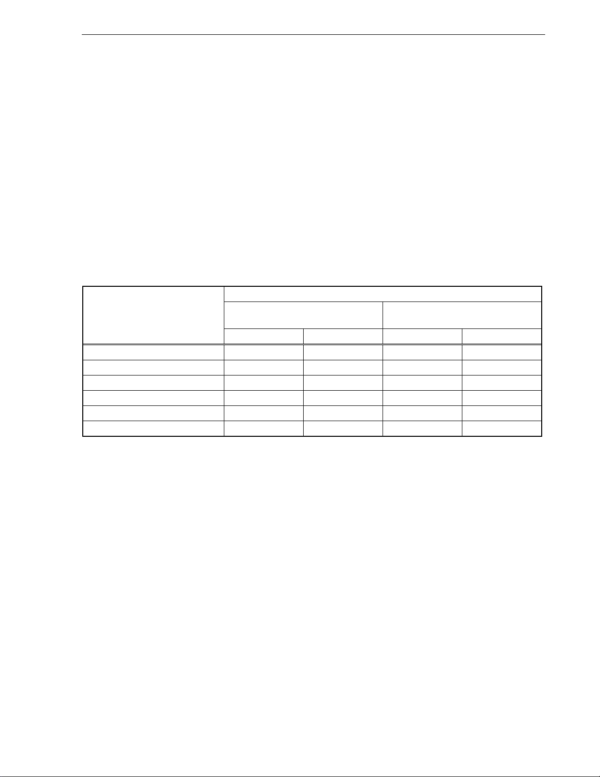
Table 1-1. Processing Time and Acknowledging Interrupt (with internal high-speed oscillator)
Library Name
self programming start library 4.25 Not acknowledged
initialize library 977.75 443.5 Not acknowledged
mode check library 753.875 753.125 219.625 218.875 Not acknowledged
block blank check library 12770.875 12765.875 12236.625 12231.625 Acknowledged
block erase library 36909.5 356318 36904.5 356296.25 36363.25 355771.75 36358.25 355750 Acknowledged
word write library
block verify library 25618.875 25613.875 25072.625 25067.625 Acknowledged
self programming end library 4.25 Not acknowledged
get information library
(option value: 03H)
get information library
(option value: 04H)
get information library
(option value: 05H)
set information library 105524.75 790809.375 105523.75 790808.375 104978.5 541143.125 104977.5 541142.125 Acknowledged
EEPROM write library
1214
(1214.375)
1496.5
(1496.875)
Remark Values in parentheses are when the write start address structure is placed outside of internal high-speed RAM.
Processing Time (unit: microseconds)
Outside short direct addressing range In short direct addressing range
Normal model Static model Normal model Static model
Min Max Min Max Min Max Min Max
2409
(2409.375)
871.25
(871.375)
863.375
(863.5)
1042.75
(1043.625)
2691.5
(2691.875)
1207
(1207.375)
(866.125)
(1038.375)
1489.5
(1489.875)
(2402.375)
866
858.125
(858.25)
1037.5
(2684.875)
2402
2684.5
679.75
(680.125)
(337.125)
(503.125)
962.25
(962.625)
337
329.125
(239.25)
502.25
1874.75
(1875.125)
2157.25
(2157.625)
672.75
(673.125)
(331.875)
(497.875)
955.25
(955.625)
1867.75
(1868.125)
331.75
323.875
(324)
497
2150.25
(2150.625)
Acknowledging
Acknowledged
Not acknowledged
Not acknowledged
Not acknowledged
Acknowledged
Interrupt
CHAPTER 1 GENERAL
Page 19
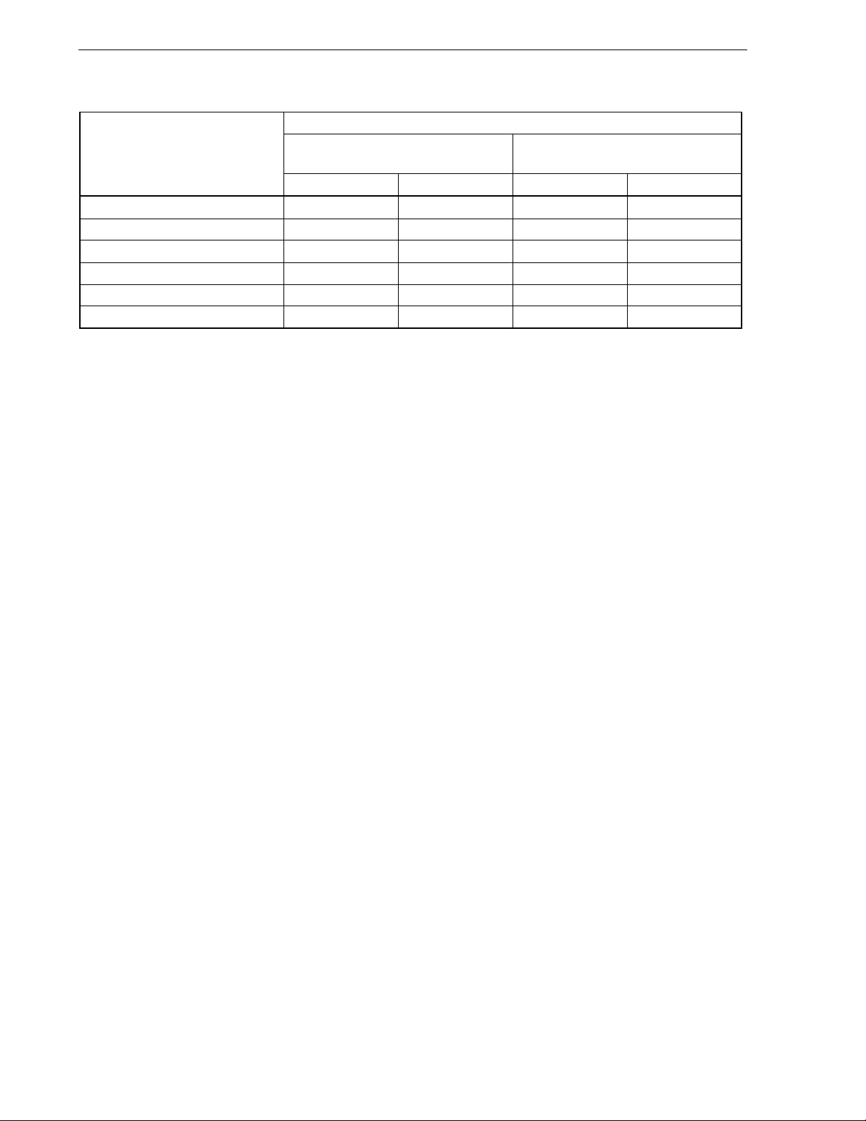
Table 1-2. Processing Time and Acknowledging Interrupt (with external system clock used)
User’s Manual U17516EJ1V0UM
Library Name
self programming start library 34/fX
initialize library 49X
mode check library 35/fX
block blank check library 174/fX
block erase library
174/f
+ 31093.875
word write library
318(321)/f
+ 644.125
block verify library 174/fX
self programming end library 34X
get information library
171(172)/f
(option value: 03H)
get information library
181(182)/f
(option value: 04H)
get information library
404(411)/f
(option value: 05H)
set information library
75/f
+ 79157.6875
EEPROM write library
318(321)/f
+ 799.875
Note fX: Operating frequency of external system clock
Remark Values in parentheses are when the write start address structure is placed outside of internal high-speed RAM.
Processing Time (unit: microseconds)
Outside short direct addressing range In short direct addressing range
Acknowledging
Normal model Static model Normal model Static model
Min Max Min Max Min Max Min Max
Note
Not acknowledged
Note
+ 485.8125 49/fX
Note
+ 374.75 29/fX
Note
+ 6382.0625 134/fX
Note
X
174/f
Note
X
+
298948.125
Note
X
318(321)/f
Note
X
+ 1491.625
Note
+ 13448.5625 134/fX
Note
X
+ 432.4375 129(130)/fX
Note
X
+ 427.875 139(140)/fX
Note
X
+ 496.125 362(369)/fX
Note
X
75/f
Note
X
+ 652400
Note
X
318(321)/f
Note
X
+ 1647.375
Note
Note
Note
134/fX
+ 31093.875
262(265)/f
Note
X
+ 644.125
Note
Note
67/f
X
+ 79157.6875
262(265)/f
Note
X
+ 799.875
+ 374.75 35/fX
+ 6382.0625 174/fX
Note
134/f
X
+ 298948.125
262(265)/f
+ 1491.625
Note
X
174/f
+ 30820.75
318(321)/f
+ 383
+ 13448.5625 174/fX
Note
Not acknowledged
Note
+ 432.4375 171(172)/fX
Note
+ 427.875 181(182)/fX
Note
+ 496.125 404(411)/fX
Note
67/f
X
+ 652400
262(265)/f
+ 1647.375
X
+ 78884.5625
Note
318(321)/f
+ 538.75
75/f
X
Note
+ 113.625 29/fX
Note
+ 6120.9375 134/fX
Note
X
Note
318(321)/f
X
Note
+ 13175.4375 134/fX
Note
+ 171.3125 129(130)/fX
Note
+ 166.75 139(140)/fX
Note
+ 231.875 362(369)/fX
Note
+ 527566.875
Note
318(321)/f
X
Note
Note
174/f
X
+ 298675
+ 1230.5
Note
75/f
X
+ 1386.25
+ 224.6875 Not acknowledged
Note
+ 113.625 Not acknowledged
Note
+ 6120.9375 Acknowledged
Note
262(265)/f
X
+ 78884.5625
Note
262(265)/f
X
Note
134/f
X
+ 30820.75
X
+ 383
Note
Note
67/f
X
X
+ 538.75
Note
262(265)/f
+ 13175.4375 Acknowledged
Note
+ 171.3125 Not acknowledged
Note
Note
+ 527566.875
Note
262(265)/f
Note
134/f
X
Acknowledged
+ 298675
Note
X
Acknowledged
+ 1230.5
+ 166.75 Not acknowledged
+ 231.875 Not acknowledged
Note
67/f
X
Acknowledged
Note
X
Acknowledged
+ 1386.25
Interrupt
CHAPTER 1 GENERAL
19
Page 20
k
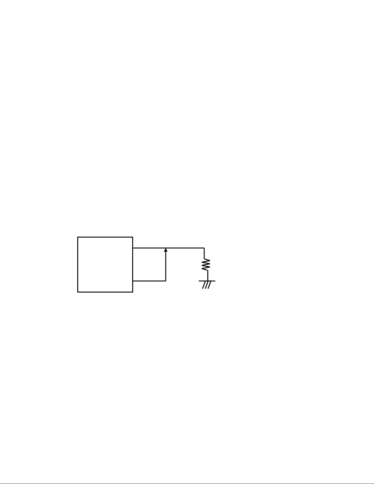
Ω
CHAPTER 2 PROGRAMMING ENVIRONMENT
This chapter explains the hardware environment and software environment necessary for the user to rewrite flash
memory by using the self programming sample library.
2.1 Hardware Environment
To execute self programming, a circuit that controls the voltage on the FLMD0 pin of the 78K0/Kx2 is necessary.
The voltage on the FLMD0 pin must be low while an ordinary user program is being executed (in normal operation
mode) and high while self programming is being executed (in flash rewriting mode).
While the FLMD0 pin is low, the firmware and software for rewriting run, but the circuit for rewriting flash memory
does not operate. Therefore, the flash memory is not actually rewritten.
A self programming sample library that makes the FLMD0 pin high is not provided. Therefore, to rewrite the flash
memory, the voltage level of the FLMD0 pin must be made high by manipulating a port throu gh user program, before
calling the self programming start library.
Here is an example of the circuit that changes the voltage on the FLMD0 pin by manipulating a port.
Figure 2-1. FLMD0 Voltage Generator
78K0/Kx2
FLMD0
Output port
10
(recommended)
20
User’s Manual U17516EJ1V0UM
Page 21
CHAPTER 2 PROGRAMMING ENVIRONMENT
2.2 Software Environment
The self programming sample library allocates its program to a user area and consumes about 500 bytes of the
program area. The self programming sample librar y itself uses the CPU (register bank 3), work area (entry RAM),
stack, and data buffer.
The following table lists the necessary software resources.
Table 2-1. Software Reso urces
Item Description Restriction
CPU Register bank 3
Work area Entry RAM: 100 bytes
Stack 39 bytes max.
Remark Use the same stack as for the
user program.
Data buffer 1 to 256 bytes
Remark The size of this buffer varies
depending on the writing unit
specified by the user program.
Program area
Normal model: 525 bytes
Static model: 432 bytes
Remark Supplied as an
assembly-language source.
Internal high-speed RAM outside short addressing range or
internal high-speed RAM in short direct addressing range with
first address as FE20H (Refer to 2.2.1 Entry RAM.)
Internal high-speed RAM other than FE20H to FE83H (Refer to
2.2.2 Stack and data buffer.)
Internal high-speed RAM other than FE20H to FE83H (Refer to
2.2.2 Stack and data buffer.)
Within 0000H to 7FFFH (32 KB)
Caution The self programming sample library and the
user program that calls the self programming
sample library must always be located within the
above range, because the firmware built into the
product is allocated to addresses starting from
8000H.
Cautions 1. The self programming operation is not guaranteed if the user manipulates the above
resources. Do not manipulate these resources during a self programming operation.
2. The user must release the above resources used by the self programming sample library
before calling the self programming sample library.
−
User’s Manual U17516EJ1V0UM
21
Page 22
CHAPTER 2 PROGRAMMING ENVIRONMENT
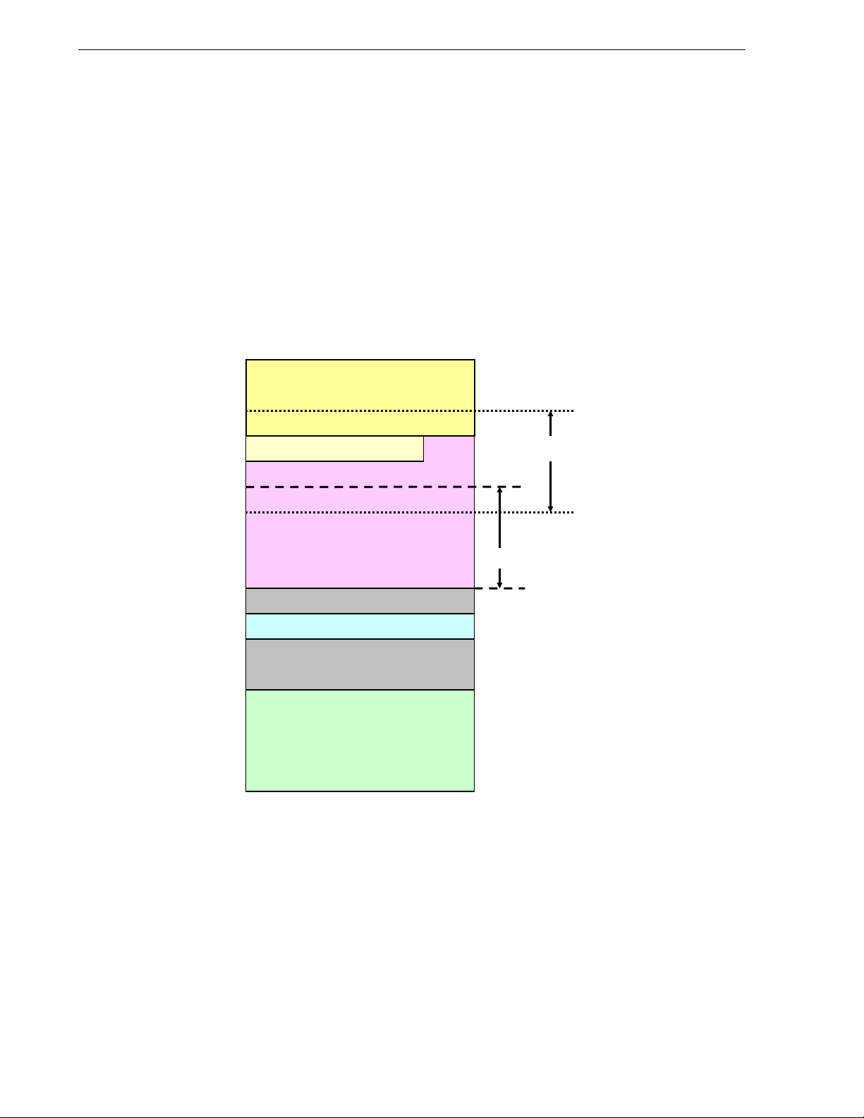
2.2.1 Entry RAM
The self programming sample library uses a work area of 100 bytes. This area is called entry RAM.
As the entry RAM, 100 bytes are automatically allocated, star ting from the first address that is specified when th e
initialize library is called. Therefore, the first address of the entry RAM can be specified in the range from FB00H to
FE20H.
In addition, a data buffer used by the initialize library to actually write data to the flash memory must be allocated to
an area that is within the range from 1 to 256 bytes and is other than the work area. For details on the data buffer,
refer to 2.2.2 Stack and data buffer.
The range in which the entry RAM can be allocated is shown below.
Figure 2-2. Allocation Range of Entry RAM
FFFFH
FF20H
FF00H
FEFFH
Special function registers (SFRs)
256 bytes
General-purpose registers
32 bytes
Short direct addressing
FE83H
FE20H
FB00H
FAFFH
FA20H
FA00H
F9FFH
F800H
F7FFH
Internal high-speed RAM
1024 bytes
Use prohibited
Buffer RAM 32 bytes
Use prohibited
Entry RAM allocation range
Internal expansion high-speed RAM
1024 bytes
Caution The size of the internal expansion high-speed RAM varies depending on the product.
For the size of the internal expansion high-speed RAM, refer to the user’s manual of each
product.
22
User’s Manual U17516EJ1V0UM
Page 23
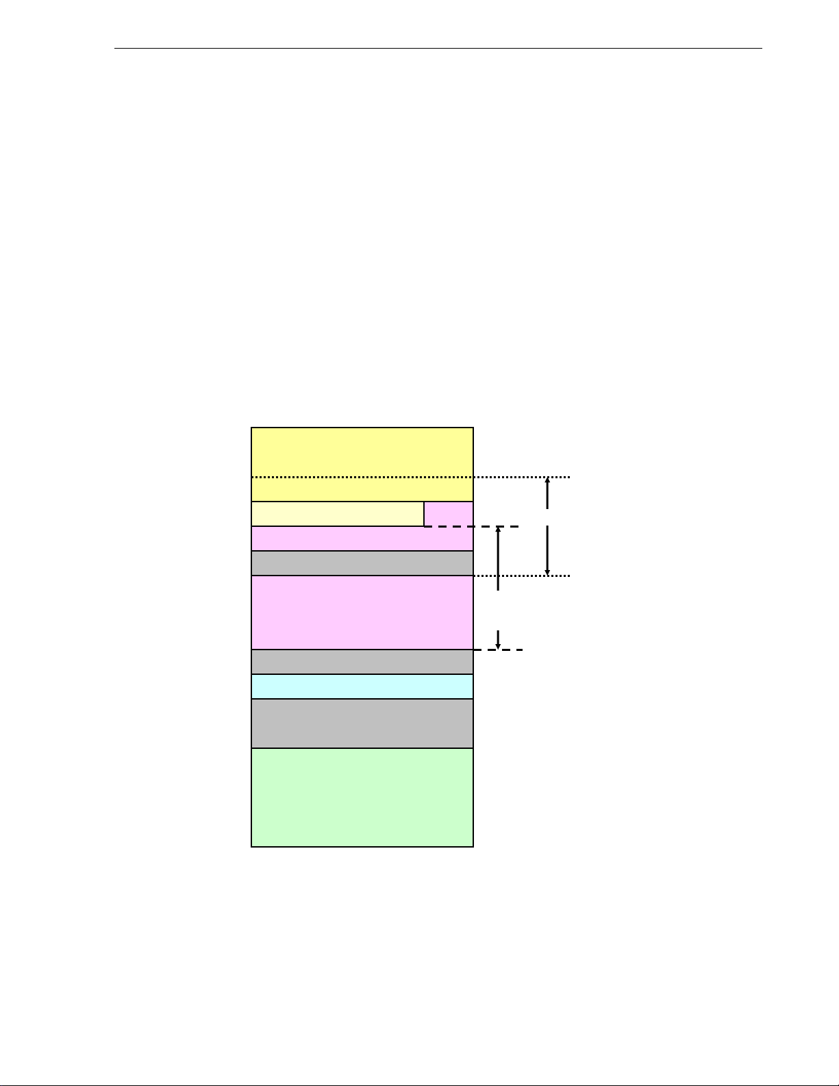
CHAPTER 2 PROGRAMMING ENVIRONMENT
2.2.2 Stack and data buffer
The self programming sample library writes data to flash memory by using the CPU. Therefore, a self
programming operation is performed by using the stack specified by the user program.
The stack must be allocated by stack processing of the self programming operation so that the entry RAM and the
RAM used by the user are not cleared. Therefore, the stack can be allocated in the internal high-speed RAM at
addresses other than FE20H to FE83H.
A data buffer is automatically allocated from the first address and by the number of data specified when the word
write library is called. Therefore , the first address of the data b uffer can be specified in the internal high-speed RAM at
an address other than FE20H to FE83H, just as for the stack pointer.
Note that data to be written to the flash memory must be appropri ately set and processed before the word write
library is called.
The following figure shows the range in which the stack pointer and data buffer can be allocated.
Figure 2-3. Allocatable Range for Stack Pointer and Data Buffer
FFFFH
FF20H
FF00H
FEFFH
Special function registers (SFRs)
256 bytes
General-purpose registers
32 bytes
Short direct addressing
FE83H
FE20H
Use prohibited
FB00H
FAFFH
FA20H
FA00H
F9FFH
F800H
F7FFH
Internal high-speed RAM
1024 bytes
Use prohibited
Buffer RAM 32 bytes
Use prohibited
Range where stack and data buffer can be
allocated (except FE20H to FE83H)
Internal expansion high-speed RAM
1024 bytes
Caution The size of the internal expansion high-speed RAM varies depending on the product.
For the size of the internal expansion high-speed RAM, refer to the user’s manual of each
product.
User’s Manual U17516EJ1V0UM
23
Page 24

CHAPTER 3 INTERRUPT SERVICING DURING SELF
PROGRAMMING
3.1 Overview
An interrupt can be generated, even while self programming is executed, in some self progr amming sample libraries
of the 78K0/Kx2.
However, unlike the case for an ordinary interrupt, the user must decide whether the processing that has been
interrupted should be resumed, by checking the return value from the self programming sample library.
24
User’s Manual U17516EJ1V0UM
Page 25
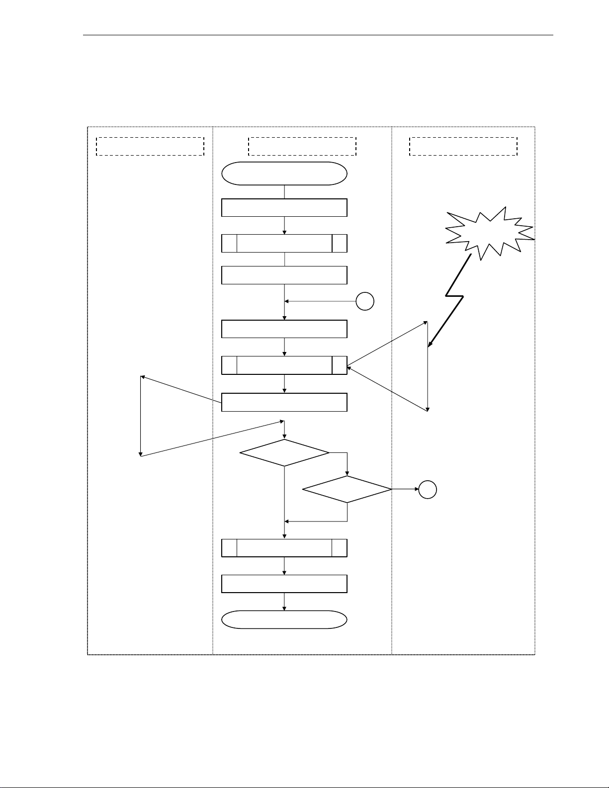
CHAPTER 3 INTERRUPT SERVICING DURING SELF PROGRAMMING
The following figure illustrates the flow of processing if an interrupt is generated while processing of the self
programming sample library is being executed.
Figure 3-1. Flow of Processing in Case of Interrupt
User program Library Interrupt handler
Self programming starts.
FLMD0 pin: Low → High
Interrupt
FlashStart
Setting of operating environment
occurs.
Servicing starts.
Servicing ends.
DI
Calling library
EI
Return value
End
FlashEnd
FLMD0 pin: High → Low
1
Stopped (= 1FH)
Retry?
No
Servicing starts.
Processing is stopped.
Yes
1
End of self programming
User’s Manual U17516EJ1V0UM
25
Page 26
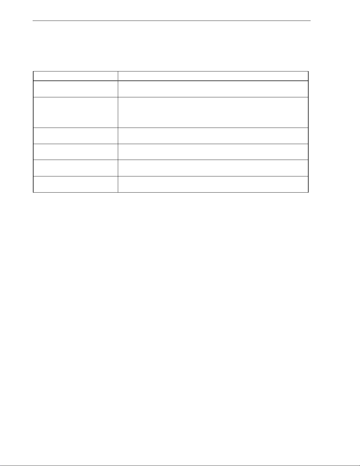
CHAPTER 3 INTERRUPT SERVICING DURING SELF PROGRAMMING
The following table shows how the processing of the self programming sample libraries that acknowledge interrupts
is resumed after the processing has been stopped by the occurrence of an interrupt.
Table 3-1. Resume Processing Stopped by Interrupt
Library Name Resuming Method
block blank check library
block erase library
word write library
block verify library
set information library
EEPROM write library
Call the block blank check library FlashBlockBlankCheck to resume processing to check
block erasure that has been stopped by the occurrence of an interrupt.
To resume processing to erase blocks that was stopped by the occurrence of an
interrupt, call the block blank check library FlashBlockBlankCheck and check whether
blocks that should be erased have been erased. Then, call the block erase library
FlashBlockErase.
Call the word write library FlashWordWrite to resume data write processing that was
stopped by the occurrence of an interrupt.
Call the block verify library FlashBlockVerify to resume block verify processing that was
stopped by the occurrence of an interrupt.
Call the set information library FlashSetInfo to resume flash information setting
processing that was stopped by the occurrence of an interrupt.
Call the EEPROM write library FlashEEPROMWrite to resume processing to write data
during EEPROM emulation that was stopped by the occurrence of an interrupt.
Remark An interrupt is not acknowledged until all of the processing of the above self programming sample
libraries has been completed, because these libraries execute their processing with interrupts disabled.
26
User’s Manual U17516EJ1V0UM
Page 27
CHAPTER 3 INTERRUPT SERVICING DURING SELF PROGRAMMING
3.2 Interrupt Response Time
Unlike the case for an ordinary interrupt, generation of an interrupt during execution of self programming is
accomplished via post-interrupt serv icing in the self programming sample library (such as setting 0x 1F as the return
value from the self programming sample library). Consequently, the response time is longer than that for an ordinary
interrupt.
When an interrupt occurs during self programming execution, both the interrupt response time of the self
programming sample library, as well as the interrupt response time of the device used, are necessary.
Remark For the response time of each device, refer to the user’s manual of each device.
Table 3-2 and Table 3-3 show the interrupt response time of the self programming sample library. Table 3-2 is a
case where the internal high-speed oscillator is used to generate the main system clock, and Table 3-3 is a case where
an external system clock is used as the main system clock.
Table 3-2. Interrupt Response Time (with Internal High-Speed Oscillator)
Interrupt Response Time (Unit: Microseconds)
Library Name
block blank check library 391.25 1300.5 81.25 727.5
block erase library 389.25 1393.5 79.25 820.5
word write library 394.75 1289.5 84.75 716.5
block verify library 390.25 1324.5 80.25 751.5
set information library 387 852.5 77 279.5
EEPROM write library 399.75 1395.5 89.75 822.5
Entry RAM outside short direct addressing
range
Min Max Min Max
Remark An interrupt is not acknowledged until all of the processing of the above self programming sample
libraries has been completed, because these libraries execute their processing with interrupts disabled.
Entry RAM inside short direct addressing
range (from FE20H)
User’s Manual U17516EJ1V0UM
27
Page 28
CHAPTER 3 INTERRUPT SERVICING DURING SELF PROGRAMMING
Table 3-3. Interrupt Response Time (with External System Clock)
Interrupt Response Time (Unit: Microseconds)
Library Name
Entry RAM outside short direct addressing
range
Entry RAM inside short direct addressing
range (from FE20H)
Min Max Min Max
block blank check library 18/fx
block erase library 18/fx
word write library 22/fx
block verify library 18/fx
set information library 16/fx
EEPROM write library 22/fx
Note
+ 192 28/fx
Note
+ 186 28/fx
Note
+ 189 28/fx
Note
+ 192 28/fx
Note
+ 190 28/fx
Note
+ 191 28/fx
Note
+ 698 18/fx
Note
+ 745 18/fx
Note
+ 693 22/fx
Note
+ 709 18/fx
Note
+ 454 16/fx
Note
+ 783 22/fx
Note
+ 55 28/fx
Note
+ 49 28/fx
Note
+ 52 28/fx
Note
+ 55 28/fx
Note
+ 53 28/fx
Note
+ 54 28/fx
Note
+ 462
Note
+ 509
Note
+ 457
Note
+ 473
Note
+ 218
Note
+ 547
Note fX: Operating frequency of external system clock
Remark An interrupt is not acknowledged until all of the processing of the above self programming sample
libraries has been completed, because these libraries execute their processing with interrupts disabled.
28
User’s Manual U17516EJ1V0UM
Page 29

CHAPTER 3 INTERRUPT SERVICING DURING SELF PROGRAMMING
3.3 Description Example
This section shows an example of writing a user program that resumes erase processing that was stopped by the
occurrence of an interrupt during execution of a self programming sample library (block erase library).
User’s Manual U17516EJ1V0UM
29
Page 30

CHAPTER 3 INTERRUPT SERVICING DURING SELF PROGRAMMING
ERS_RTRY:
; Main processing
MOV A, #0 ; Sets 0 as the bank number of the block to be erased.
MOV B, #10 ; Sets 10 as the block number of the block to be erased.
DI ; Disables interrupts.
CALL !_FlashBlockErase ; Calls the block erase library.
EI ; Enables interrupts.
CMP A, #1FH ; Checks whether a stop status is set.
BZ $BLN_RTRY ; If the stop status is set,
; jumps to resume processing BLN_RTRY.
CMP A, #00H ; Checks whether execution has been correctly
completed.
BNZ $ERS_FALSE_END ; Jumps to abnormal termination ERS_FALSE_END if
execution has not been correctly completed.
BR ERS_TRUE_END
BLN_RTRY:
; Resume processing
MOV A, #0 ; Sets 0 as the bank number of the block to be
blank-checked.
MOV B, #10 ; Sets 10 as the block number of the block to be
blank-checked.
DI ; Disables interrupts.
; Calls the block blank check library.
CALL !_FlashBlockBlankCheck
EI ; Enables interrupts.
CMP A, #1FH ; Checks whether a stop status is set.
BZ $BLN_RTRY ; If the stop status is set,
; retries the resume processing.
CMP A, #00H ; Checks whether execution has been correctly
completed.
BNZ $ERS_RTRY ; Retries the main processing if execution has not been
correctly completed.
; Clears the internal status of the stop processing
MOVW AX, #EntryRAM ; Sets the first address of entry RAM.
CALL !_FlashEnv ; Calls the initialize library.
ERS_TRUE_END:
; Normal completion
ERS_FALSE_END:
; Abnormal termination
Caution It is assumed that the entry RAM has already been set.
30
User’s Manual U17516EJ1V0UM
Page 31

CHAPTER 3 INTERRUPT SERVICING DURING SELF PROGRAMMING
3.4 Cautions
This section explains points to be noted during interrupt servicing.
− If processing related to self programming is performed or a setting related to it is changed during processing of an
interrupt that has occurred during execution of self programming, then the operation is not guaranteed. Do not
perform processing related to self programming and change settings related to it during interrupt servicing.
− Do not use register bank 3 during interrupt servicing, because self programming uses register bank 3.
− Save and restore registers used for interrupt servicing during interrupt servicing.
− If the set time of the watchdog timer is too short, processing of the set information library may not be completed.
Therefore, do not set a time that is too short to the watchdog timer.
If an interrupt successively occurs during a specific period while processing of the set information library is being
executed, an infinite loop may occur if processing of the set information library is resumed after it has been stopped
by the interrupt, because the processing is started from the beginning. Therefore, do not allow an interrupt to occur
successively at an interval shorter than that within which processing of the set information library is to be completed.
Remark Processing time of set information library (at 8 MHz)
Min.: 108 milliseconds
Max.: 696 milliseconds
− If multiple interrupts occur during execution of self programming, then the operation is not guaranteed. Disable the
acknowledging of multiple interrupts during execution of self programming.
− If processing of the self programming sample library that was stopped by the occurrence of an interrupt is not
resumed and processing of another block is to be performed, then the initialize library must be called before the
processing of another block is started.
Example To not resume erase processing of block 0 that was stopped and to execute erase processing of block 1,
call the initialize library and then start the erase processing of block 1.
− Do not erase the entry RAM, stack, and data buffer until the series of processing tasks has been completed.
− Allocate an interrupt servicing program in an area other than that of the blocks to be rewritten, just as for the self
programming program.
User’s Manual U17516EJ1V0UM
31
Page 32

CHAPTER 4 BOOT SWAP FUNCTION
If rewriting of the vector table data, the basic functions of the program, or the self progr amming area f ails because of
a momentary power failure or the occurrence of a reset due to an external cause, then the data being rewritten is lost,
the user program cannot be restarted by a reset, and rewriting c an no longer be performed. This problem can be
avoided by using a boot swap function through self programming.
The boot swap function is to replace boot program area, boot cluster 0
cluster 1
Note
.
Before rewrite processing is started, a new boot program is written to boot cluster 1. This boot cluster 1 and boot
cluster 0 are swapped and boot cluster 1 is used as a boot program area.
As a result, even if a power f ailure occurs while the boot program area is rewritten, the program is ex ecuted correctly
because the next reset start program is booted from boot cluster 1. After that, boot cluster 0 can be erased or written
as necessary.
Note Boot cluster 0 (0000H to 0FFFH): Original boot program area
Boot cluster 1 (1000H to 1FFFH): Boot swap target area
Note
, with the boot swap target area, boot
32
User’s Manual U17516EJ1V0UM
Page 33

CHAPTER 4 BOOT SWAP FUNCTION
Figure 4-1 shows the flow of boot swapping by using the self programming sample library.
Figure 4-1. Flow of Boot Swapping
Boot swapping starts
<1>
<2> <9>
<3> <10>
<4> <11>
<5> <12>
<6> <13>
Preprocessing
FlashBlockErase
Normal
completion?
Yes
FlashWordWrite
Normal
completion?
Yes
FlashBlockVerify
Normal
completion?
Yes
FlashGetInfo
Normal
completion?
Yes
FlashSetInfo
1
No
No
No
No
No
No
1
<7> <14>
<8> <15>
<16>
Normal
completion?
Yes
Reset
Cluster 1
completed?
Yes
Post-processing
Boot swapping ends
User’s Manual U17516EJ1V0UM
33
Page 34

CHAPTER 4 BOOT SWAP FUNCTION
r
<1> Preprocessing
The following preprocessing of boot swapping is performed.
− Setting of hardware environment
− Declaring start of self programming
− Setting of software environment
− Initializing entry RAM
− Checking voltage level
<2> Erasing boot cluster 1
Blocks 4 to 7 are erased by calling the block erase library FlashBlockErase.
Remark The block erase library erases each block one by one.
Boot cluster 1
Normal operation mode
1FFFH
Program area
0
1000H
0FFFH
0800H
07FFH
0081H
0080H
007FH
003FH
0000H
CALLF entry
2048 bytes
Program area
1919 bytes
Option byte
CALLT table 64 bytes
Vector table 64 bytes
Boot cluste
1FFFH
1C00H
1800H
1400H
1000H
0FFFH
0800H
07FFH
0081H
0080H
007FH
003FH
0000H
Block 7 (erased)
Block 6 (erased)
Block 5 (erased)
Block 4 (erased)
CALLF entry
2048 bytes
Program area
1919 bytes
Option byte
CALLT table 64 bytes
Vector table 64 bytes
34
User’s Manual U17516EJ1V0UM
Page 35

CHAPTER 4 BOOT SWAP FUNCTION
<3> Copying boot cluster 0
The contents of 0000H to 0FFFH are written to 1000F to 1FFFH by calling the word write library FlashWordWrite.
Remark The word write library writes data in word units (256 bytes max.).
1FFFH
Copies contents of 0000H
to 0FFFH.
1000H
0FFFH
0800H
07FFH
0081H
0080H
007FH
003FH
0000H
CALLF entry
2048 bytes
Program area
1919 bytes
Option byte
CALLT table 64 bytes
Vector table 64 bytes
<4> Verifying boot cluster 1
Blocks 4 to 7 are verified by calling the block verify library FlashBlockVerify.
Remark The block verify library verifies each block one by one.
<5> Reading set status of boot swapping
The set status of boot swapping can be read by calling the get information library FlashGetInfo.
User’s Manual U17516EJ1V0UM
35
Page 36

CHAPTER 4 BOOT SWAP FUNCTION
Bi
4
Bit 3
Bit 2
Bit 1
Bit 0
<6> Setting of boot swap bit
Set the boot swap bit to “execute boot swapping (0)” by calling the set information library FlashSetInfo.
t 7 Bit 6 Bit 5 Bit
−
− 1 − 1 1 1 0
Bit 0: Executes (0)/Does not execute (1) boot swapping.
Bit 1: Disables (0)/Enables (1) chip erasure.
Bit 2: Disables (0)/Enables (1) block erasure.
Bit 3: Disables (0)/Enables (1) writing.
Bit 5: Disables (0)/Enables (1) boot area rewriting.
<7> Occurrence of event
Boot cluster 1 is used as a boot program area when an external reset or overflow of the watchdog timer is
generated.
<8> End of swap processing (boot cluster 1)
Operations <2> to <7> complete the swap processing of boot cluster 1
<9> Erasing boot cluster 0
Blocks 0 to 3 are erased by calling the block erase library FlashBlockErase.
Remark The block erase library erases each block one by one.
1FFFH
17FFH
1081H
1080H
107FH
1000H
0FFFH
0C00H
0800H
04000H
0000H
CALLF entry
2048 bytes
Program area
1919 bytes
Option byte
CALLT table 64 bytes
Vector table 64 bytes
Block 3 (erased)
Block 2 (erased)
Block 1 (erased)
Block 0 (erased)
Boot program area
36
User’s Manual U17516EJ1V0UM
Page 37

CHAPTER 4 BOOT SWAP FUNCTION
<10> Writing new program to boot cluster 0
The contents of the new program are written to 0000H to 0FFFH by calling the word write library
FlashWordWrite.
Remark The word write library writes the program in word units (256 bytes max.).
1FFFH
17FFH
1081H
1080H
107FH
1000H
0FFFH
0C00H
0800H
04000H
0000H
CALLF entry
2048 bytes
Program area
1919 bytes
Option byte
CALLT table 64 bytes
Vector table 64 bytes
Block 3 (written)
Block 2 (written)
Block 1 (written)
Block 0 (written)
Boot program area
<11> Verifying boot cluster 0
Blocks 0 to 3 are verified by calling the block verify library FlashBlockVerify.
Remark The block verify library verifies each block one by one.
<12> Reading set status of boot swapping.
The set status of boot swapping is read by calling the get information library FlashGetInfo.
User’s Manual U17516EJ1V0UM
37
Page 38

CHAPTER 4 BOOT SWAP FUNCTION
Bi
4
Bit 3
Bit 2
Bit 1
Bit 0
<13> Setting of boot swap bit
Set the boot swap bit to “not execute boot swapping (1)” by calling the set information library FlashSetInfo.
t 7 Bit 6 Bit 5 Bit
−
− 1 − 1 1 1 1
Bit 0: Executes (0)/Does not execute (1) boot swapping.
Bit 1: Disables (0)/Enables (1) chip erasure.
Bit 2: Disables (0)/Enables (1) block eraure.
Bit 3: Disables (0)/Enables (1) writing.
Bit 5: Disables (0)/Enables (1) boot area rewriting.
<14> Occurrence of event
Boot cluster 0 is used as a boot program area when an external reset or overflow of the watchdog timer is
generated.
<15> End of swap processing (boot cluster 0)
Operations <9> to <14> complete the swap processing of boot cluster 0.
<16> Post-processing
As post-processing of boot swapping, the following is performed.
− Declaring end of self programming
− Setting of hardware environment
38
User’s Manual U17516EJ1V0UM
Page 39

CHAPTER 5 SELF PROGRAMMING SAMPLE LIBRARY
This chapter explains details on the self programming sample library.
For the source program of each library, refer to APPENDIX A SAMPLE PROGRAM.
5.1 Type of Self Programming Sample Library
The self programming sample library consists of the following libraries.
Table 5-1. Self programming sample library List
Library Name
self programming start library
initialize library
mode check library
block blank check library
block erase library
word write library
block verify library
self programming end library
get information library
Call Example (C language)
Call Example (assembly language)
FlashStart();
CALL !_FlashStart
FlashEnv( &EntryRAM[0] );
CALL !_FlashEnv
Status = CheckFLMD( );
CALL !_CheckFLMD
Status = FlashBlockBlankCheck(BlankCheckBANK,
BlankCheckBlock );
CALL !_FlashBlockBlankCheck
Status = FlashBlockErase( EraseBANK, EraseBlock );
CALL !_FlashBlockErase
Status = FlashWordWrite( &WordAddr, WordNumber,
&DataBuffer );
CALL !_FlashWordWrite
Status = FlashBlockVerfy( VerifyBANK, VerifyBlock );
CALL !_FlashBlockVerify
FlashEnd( );
CALL !_FlashEnd
Status = FlashGetInfo( &GetInfo, &DataBuffer );
Outline
Declares start of self
programming.
Initializes entry RAM.
Checks voltage level.
Checks erasing of specified
block (1 KB).
Erases specified library (1
KB).
Writes 1- to 64-word data to
specified address.
Verifies specified block (1
KB) (internal verification).
Declares end of self
programming.
Reads flash information.
set information library
EEPROM write library
CALL !_FlashGetInfo
Status = FlashSetInfo( SetInfoData );
CALL !_FlashSetInfo
Status = FlashEEPROMWrite( &WordAdder,
WordNumber, &DataBuffer );
CALL !_EEPROMWrite
User’s Manual U17516EJ1V0UM
Changes setting of flash
information.
Writes 1- to 64-word data to
specified address (during
EEPROM emulation).
39
Page 40

CHAPTER 5 SELF PROGRAMMING SAMPLE LIBRARY
5.2 Explanation of Self Programming Sample Library
Each self programming sample library is explained in the following format.
self programming sample library name
[Outline]
Outlines the function of the self programming sample library.
[Format]
Indicates a format to call the self programming sample library from a user program described in C or an assembly
language.
Caution In this manual, the data type name is defined as follows.
Definition Name Data Type
UCHAR unsigned char
USHORT unsigned short
[Argument]
Indicates the argument of the self programming sample library.
[Return value]
Indicates the return value from the self programming sample library.
[Function]
Indicates the function details and points to be noted for the self programming sample library.
[Register status after calling]
Indicates the status of registers after the self programming sample library is called.
[Stack size]
Indicates the size of the stack used by the self programming sample library.
[ROM capacity]
Indicates the ROM capacity necessary for self programming.
[Call example]
Indicates an example of calling the self programming sample library from a user program described in C or an
assembly language.
[Supplement]
Indicates supplementary information on a self programming sample library other than the above.
[Flow]
This indicates the program flow of the self programming sample library.
40
User’s Manual U17516EJ1V0UM
Page 41

CHAPTER 5 SELF PROGRAMMING SAMPLE LIBRARY
self programming start library
[Outline]
Declares the start of self programming.
[Format]
<C language>
void FlashStart( void )
<Assembly language>
CALL !_FlashStart
[Argument]
None
[Return value]
None
[Function]
This self programming sample library declares the start of self programming.
Therefore, call this library first as a self programming operation.
Caution The operation is not guaranteed if this library is called with interrupts enabled. Before calling
this library, execute the DI instruction, and execute the EI instruction after execution of this
library is completed, so that acknowledgment of an interrupt is disabled while this library is
executed.
[Register status after calling]
No register is cleared.
[Stack size]
0 bytes
[ROM capacity]
12 bytes
[Call example]
<C language>
di(); /* Disables interrupts. */
FlashStart(); /* Calls self programming start library. */
ei(); /* Enables interrupts. */
<Assembly language>
DI ; Disables interrupts.
CALL !_FlashStart ; Calls self programming start library.
EI ; Enables interrupts.
User’s Manual U17516EJ1V0UM
41
Page 42

CHAPTER 5 SELF PROGRAMMING SAMPLE LIBRARY
[Flow]
Figure 5-1 shows the flow of the self programming start library.
Figure 5-1. Flow of Self Programming Start Library
FlashStart
library
Switch to self
programming mode
End
42
User’s Manual U17516EJ1V0UM
Page 43

CHAPTER 5 SELF PROGRAMMING SAMPLE LIBRARY
initialize library
[Outline]
Initializes entry RAM.
[Format]
<C language>
void FlashEnv( USHORT EntryRAM )
<Assembly language>
CALL !_FlashEnv
[Argument]
<C language>
Argument Explanation
USHORT EntryRAM First address of entry RAM
<Assembly language>
Argument Explanation
AX First address of entry RAM
Note For details on entry RAM, refer to 2.2.1 Entry RAM.
[Return value]
None
[Function]
This self programming sample library secures and initializes the entry RAM used for self programming.
As initialize processing, this library secures 100 bytes from an address specified by th e parameter as a work area
where the flash memory writing firmware operates, and sets the initial value to the first address +06H to +16H. The
other areas are cleared to 0.
Remark Call this library after calling the self programming start library.
Also call this library to resume processing of a library executing self programming that was stopped by
the occurrence of an interrupt.
[Register status after calling]
No register is cleared.
[Stack size]
30 bytes
[ROM capacity]
11 bytes
Note
Note
User’s Manual U17516EJ1V0UM
43
Page 44

CHAPTER 5 SELF PROGRAMMING SAMPLE LIBRARY
[Call example]
<C language>
USHORT EntryRAM; /* Declares variable. */
FlashEnv( &EntryRAM[0] ); /* Calls initialize library. */
<Assembly language>
SELF_RAM DSEG AT 0FDBCH
EntryRAM: DS 100
SELF_PROG CSEG
MOVW AX, #EntryRAM ; Sets first address of entry RAM.
CALL !_FlashEnv ; Calls initialize library.
Caution Allocate the entry RAM at any address of the internal high-speed RAM outside of the short direct
addressing range.
To allocate it in the internal high-speed RAM in the short direct addressing range, the first
address is set to FE20H.
[Flow]
Figure 5-2 shows the flow of the initialize library.
Figure 5-2. Flow of Initialize Library
FlashEnv
library
Save to PSW stack
Set to register bank 3
Set entry RAM parameter to HL
Register bank recovery through
PSW recovered from stack
register
Set 00H to C register
CALL 8100H
End
44
User’s Manual U17516EJ1V0UM
Page 45

CHAPTER 5 SELF PROGRAMMING SAMPLE LIBRARY
mode check library
[Outline]
Checks the voltage level.
[Format]
<C language>
UCHAR CheckFLMD( void )
<Assembly language>
CALL !_CheckFLMD
[Argument]
None
[Return value]
Status Explanation
00H
01H
Remark The status is the UCHAR type in C and is stored in the A register in an assembly language.
[Function]
This library checks the voltage level (high or low) of the FLMD0 pin.
Remark Call this library after calling the self programming start library to check the voltage level of the FLMD0
pin.
Caution If the FLMD0 pin is at low level, operations such as erasing and writing the flash memory cannot
be performed. To manipulate the flash memory by self programming, it is necessary to call this
library and confirm that the FLMD0 pin is at high level.
[Register status after calling]
Memory Model Register Status
Normal model
Static model
[Stack size]
28 bytes
Normal completion
− FLMD0 pin is at high level.
Abnormal termination
− FLMD0 pin is at low level.
Registers cleared: A, BC
Registers held: X, DE, HL
Registers cleared: A
Registers held: X, BC, DE, HL
User’s Manual U17516EJ1V0UM
45
Page 46

CHAPTER 5 SELF PROGRAMMING SAMPLE LIBRARY
[ROM capacity]
Memory Model ROM Capacity
Normal model 14 bytes
Static model 11 bytes
[Call example]
<C language>
UCHAR Status; /* Declares variable.*/
Status = CheckFLMD(); /* Calls mode check library and */
/* stores status information. */
<Assembly language>
SELF_RAM DSEG
Status: DS 1
SELF_PROG CSEG
CALL !_CheckFLMD ; Calls mode check library.
MOV !Status, A ; Stores status information.
[Flow]
Figure 5-3 shows the flow of the mode check library.
Figure 5-3. Flow of Mode Check Library
CheckFLMD
library
Save to PSW stack
Set to register bank 3
Set 0EH to C register
CALL 8100H
Register bank recovery through
PSW recovered from stack
Set B register in register bank
3 to C register (normal mode)
or A register (static mode) in
register bank
End
46
User’s Manual U17516EJ1V0UM
Page 47

CHAPTER 5 SELF PROGRAMMING SAMPLE LIBRARY
block blank check library
[Outline]
Checks erasing of a specified block (1 KB).
[Format]
<C language>
UCHAR FlashBlockBlankCheck( UCHAR BlankCheckBANK, UCHAR BlankCheckBlock )
<Assembly language>
CALL !_FlashBlockBlankCheck
[Argument]
<C language>
Argument Explanation
UCHAR BlankCheckBANK Bank number of block to be blank-checked.
UCHAR BlankCheckBlock Block number of block to be blank-checked.
<Assembly language>
Argument Explanation
A Bank number of block to be blank-checked.
B Block number of block to be blank-checked.
Remark Set the bank number to 0 when a product with which no bank number has to be set is used.
[Return value]
Status Explanation
00H
05H
1BH
1FH
Remark The status is the UCHAR type in C and is stored in the A register in an assembly language.
Normal completion
Specified block is blank (erase processing has been completed).
Parameter error
Specified bank number or block number is outside the settable range.
Blank check error
Specified block is not blank (erase processing has not been completed).
Processing is stopped because an interrupt occurs.
An interrupt occurs while processing of this library is under execution.
User’s Manual U17516EJ1V0UM
47
Page 48

CHAPTER 5 SELF PROGRAMMING SAMPLE LIBRARY
[Function]
This library checks if a specified block (1 KB) has been erased.
Remark Because only one block is checked at a tim e, call this library as many times as required to check two or
more blocks.
Caution The operation is not guaranteed if this library is called with interrupts enabled. Before calling
this library, execute the DI instruction, and execute the EI instruction after execution of this
library is completed, so that acknowledgment of an interrupt is disabled while this library is
executed.
[Register status after calling]
Memory Model Register Status
Normal model
Static model
Registers cleared: AX, BC
Registers held: DE, HL
Registers cleared: A, BC
Registers held: X, DE, HL
[Stack size]
Memory Model Stack Size
Normal model 37 bytes
Static model 35 bytes
[ROM capacity]
Memory Model ROM Capacity
Normal model 67 bytes (of which 30 bytes are common routine)
Static model 54 bytes (of which 30 bytes are common routine)
48
User’s Manual U17516EJ1V0UM
Page 49

CHAPTER 5 SELF PROGRAMMING SAMPLE LIBRARY
[Call example]
<C language>
UCHAR Status; /* Declares variable. */
UCHAR BlankCheckBANK; /* Declares variable. */
UCHAR BlankCheckBlock; /* Declares variable. */
BlankCheckBANK = 0; /* Sets bank number of block to be blank-checked to 0. */
BlankCheckBlock = 10; /* Sets block number of block to be blank-checked to 10. */
/* Calls block blank check library and */
/* stores status information.*/
di(); /* Disables interrupts. */
Status = FlashBlockBlankCheck ( BlankCheckBANK, BlankCheckBlock );
ei(); /* Enables interrupts. */
<Assembly language>
SELF_RAM DSEG
Status: DS 1
SELF_PROG CSEG
MOV A, #0 ; Sets bank number of block to be blank-checked to 0.
MOV B, #10 ; Sets block number of block to be blank-checked to 10.
; Calls block blank check library.
DI ; Disables interrupts.
CALL !_FlashBlockBlankCheck
MOV !Status, A ; Stores status information.
EI ; Enables interrupts.
User’s Manual U17516EJ1V0UM
49
Page 50

CHAPTER 5 SELF PROGRAMMING SAMPLE LIBRARY
[Flow]
Figure 5-4 shows the flow of the block blank check library.
Figure 5-4. Flow of Block Blank Check Library
FlashBlockBlankCheck
Calculate block number from
argument’s bank and b loc k number
Save to PSW stack
Set to register bank 3
library
Set block number to entry
Register bank recovery through
PSW recovered from stack
Set B register in register bank
3 to C register (normal mode)
or A register (static mode) in
RAM +3
Set 08H to C register
CALL 8100H
register bank
End
50
User’s Manual U17516EJ1V0UM
Page 51

CHAPTER 5 SELF PROGRAMMING SAMPLE LIBRARY
block erase library
[Outline]
Erases a specified block (1 KB).
[Format]
<C language>
UCHAR FlashBlockErase( UCHAR EraseBANK, UCHAR EraseBlock )
<Assembly language>
CALL !_FlashBlockErase
[Argument]
<C language>
Argument Explanation
UCHAR EraseBANK Bank number of block to be erased
UCHAR EraseBlock Block number of block to be erased.
<Assembly language>
Argument Explanation
A Bank number of block to be erased
B Block number of block to be erased.
Remark Set the bank number to 0 when a product with which no bank number has to be set is used.
[Return value]
Status Explanation
00H Normal completion
05H
10H
1AH
1FH
Remark The status is the UCHAR type in C and is stored in the A register in an assembly language.
Parameter error
Specified bank number or block number is outside the settable range.
Protect error
Specified block is included in the boot area and rewriting the boot area is disabled.
Erase error
An error occurred during processing of this library.
Processing is stopped by the occurrence of an interrupt.
An interrupt occurred while processing of this library was under execution.
User’s Manual U17516EJ1V0UM
51
Page 52

CHAPTER 5 SELF PROGRAMMING SAMPLE LIBRARY
[Function]
This library erases a specified block (1 KB).
Remark Because only one block is erased at a time, call this library as many times as required to erase two or
more blocks.
Caution The operation is not guaranteed if this library is called with interrupts enabled. Before calling
this library, execute the DI instruction, and execute the EI instruction after execution of this
library is completed, so that acknowledgment of an interrupt is disabled while this library is
executed.
[Register status after calling]
Memory Model Register Status
Normal model
Static model
Registers cleared: AX, BC
Registers held: DE, HL
Registers cleared: A, BC
Registers held: X, DE, HL
[Stack size]
Memory Model Stack Size
Normal model 39 bytes
Static model 37 bytes
[ROM capacity]
Memory Model ROM Capacity
Normal model 67 bytes (of which 30 bytes are common routine)
Static model 54 bytes (of which 30 bytes are common routine)
52
User’s Manual U17516EJ1V0UM
Page 53

CHAPTER 5 SELF PROGRAMMING SAMPLE LIBRARY
[Call example]
<C language>
UCHAR Status; /* Declares variable. */
UCHAR EraseBANK; /* Declares variable. */
UCHAR EraseBlock; /* Declares variable. */
EraseBANK = 0; /* Sets bank number of block to be erased to 0. */
EraseBlock = 10; /* Sets block number of block to be erased to 10. */
di(); /* Disables interrupts. */
/* Calls block erase library and stores status */
/* information. */
Status = FlashBlockErase( EraseBANK, EraseBlock );
ei(); /* Enables interrupts. */
<Assembly language>
SELF_RAM DSEG
Status: DS 1
SELF_PROG CSEG
MOV A, #0 ; Sets bank number of block to be erased to 0.
MOV B, #10 ; Sets block number of block to be erased to 10.
DI ; Disables interrupts.
CALL !_FlashBlockErase ; Calls block erase library.
MOV !Status, A ; Stores status information.
EI ; Enables interrupts.
User’s Manual U17516EJ1V0UM
53
Page 54

CHAPTER 5 SELF PROGRAMMING SAMPLE LIBRARY
[Flow]
Figure 5-5 shows the flow of the block erase library.
Figure 5-5. Flow of Block Erase Library
Calculate block number from
argument’s bank and b loc k number
FlashBlockErase
library
Save to PSW stack
Set to register bank 3
Set block number to entry
Register bank recovery through
PSW recovered from stack
Set B register in register bank
3 to C register (normal mode)
or A register (static mode) in
RAM +3
Set 03H to C register
CALL 8100H
register bank
End
54
User’s Manual U17516EJ1V0UM
Page 55

CHAPTER 5 SELF PROGRAMMING SAMPLE LIBRARY
word write library
[Outline]
Writes 1- to 64-word data to specified addresses.
[Format]
<C language>
UCHAR FlashWordWrite( struct stWordAddress *ptr, UCHAR WordNumber,
USHORT DataBufferAddress )
<Assembly language>
CALL !_FlashWordWrite
[Argument]
<C language>
Argument Explanation
Note 1
struct stWordAddress *ptr
UCHAR WordNumber Number of data to be written (1 to 64)
USHORT DataBufferAddress First address of write data buffer
First address of write start address structure (stWordAddress)
This structure must be 3 bytes in size and at a 4-byte boundary and must be secured by
the user.
Note 2
<Assembly language>
Argument Explanation
AX
B Number of data to be written (1 to 64)
HL First address of write data buffer
First address of data having structure same as that of write start address structure
C (Refer to APPENDIX A SAMPLE PROGRAM.)
Note 2
Notes 1. Write start address structure
struct stWordAddress{
USHORT WriteAddress; /* Write start address*/
UCHAR WriteBank; /* Bank number of write start address*/
};
Remarks 1. Specify the write start address as a multiple of 4 bytes.
2. Set the bank number to 0 when a product with which no bank number has to be set is
used.
Caution Before calling this library, set a value to each member of this structure.
2. Before calling this library, set write data to the write data buffer (whose first address is indicated by
DataBufferAddress).
Caution Set the write start address and the number of data to be written so that they do not straddle over
the boundary of each block.
.
Note 1
in
User’s Manual U17516EJ1V0UM
55
Page 56

CHAPTER 5 SELF PROGRAMMING SAMPLE LIBRARY
[Return value]
Status Explanation
00H Normal completion
05H
10H
1CH
1FH
Parameter error
− Start address not is a multiple of 1 word (4 bytes).
− The number of data to be written is 0.
− The number of data to be written exceeds 64 words.
− Write end address (Start address + (Number of data to be written × 4 bytes)) exceeds
the flash memory area.
Protect error
− Specified range includes the boot area and rewriting the boot area is disabled.
Write error
− Data is verified but does not match after execution of the processing of this library.
Processing is stopped by the occurrence of an interrupt.
− An interrupt occurred while processing of this library was under execution.
Remark The status is the UCHAR type in C and is stored in the A register in an assembly language.
[Function]
This library writes the specified number of data from a specified address.
Set a RAM area containing the data to be written as a data buffer and call this library.
Data of up to 256 bytes can be written (in 4-byte units) at one time.
Remark Call this library as many times as required to write data of more than 256 bytes.
Cautions 1. After writing data, execute verification (internal verification) of the block including the range
in which the data has been written. If verification is not executed, the written data is not
guaranteed.
2. The operation is not guaranteed if this library is called with interrupts enabled. Before
calling this library, execute the DI instruction, and execute the EI instruction after execution
of this library is completed, so that acknowledgment of an interrupt is disabled while this
library is executed.
[Register status after calling]
Memory Model Register Status
Normal model
Static model
Registers cleared: AX, BC, DE
Registers held: HL
Registers cleared: AX, C
Registers held: B, DE, HL
[Stack size]
39 bytes
[ROM capacity]
Memory Model ROM Capacity
Normal model 117 bytes (of which 57 bytes are common routine)
Static model 100 bytes (of which 57 bytes are common routine)
56
User’s Manual U17516EJ1V0UM
Page 57

CHAPTER 5 SELF PROGRAMMING SAMPLE LIBRARY
[Call example]
<C language>
struct stWordAddress WordAddr; /* Declares variable. */
UCHAR DataBuffer[4]; /* Declares variable. */
UCHAR WordNumber; /* Declares variable. */
UCHAR Status; /* Declares variable. */
DataBuffer[0] = 0x11; /* Sets data to be written. */
DataBuffer[1] = 0x22; /* Sets data to be written. */
DataBuffer[2] = 0x33; /* Sets data to be written. */
DataBuffer[3] = 0x44; /* Sets data to be written. */
WordNumber = 1; /* Sets number of data to be written. */
WordAddr.WriteAddress = 0xA000; /* Sets 0xA000H as write start address. */
WordAddr.WriteBANK = 0; /* Sets bank number of write start address to 0. */
di(); /* Disables interrupts. */
/* Calls word write library and stores status */
/* information. */
Status = FlashWordWrite( &WordAddr, WordNumber, &DataBuffer );
ei(); /* Enables interrupts. */
User’s Manual U17516EJ1V0UM
57
Page 58

CHAPTER 5 SELF PROGRAMMING SAMPLE LIBRARY
<Assembly language>
SELF_RAM DSEG
DataBuffer: DS 4
WordAddr:
WriteAddress: DS 2
WriteBank: DS 1
Status: DS 1
SELF_PROG CSEG
MOV A, #11H
MOV !DataBuffer, A ; Sets data to be written.
MOV A, #22H
MOV !DataBuffer+1, A ; Sets data to be written.
MOV A, #33H
MOV !DataBuffer+2, A ; Sets data to be written.
MOV A, #44H
MOV !DataBuffer+3, A ; Sets data to be written.
MOVW AX, #0A000H
MOVW !WriteAddress, AX ; Sets 0xA000H as write start address.
MOV A, #0
MOV !WriteBANK, A ; Sets bank number of write start address to 0.
MOVW AX, #WordAddr ; Sets first address of write start address
structure.
MOV B, #1 ; Sets number of data to be written.
MOVW HL, #DataBuffer ; First address of write data buffer
DI ; Disables interrupts.
CALL !_FlashWordWrite ; Calls word write library.
MOV !Status, A ; Stores status information.
EI ; Enables interrupts.
58
User’s Manual U17516EJ1V0UM
Page 59

CHAPTER 5 SELF PROGRAMMING SAMPLE LIBRARY
[Flow]
Figure 5-6 shows the flow of the word write library.
Figure 5-6. Flow of Word Write Library
argument structure member’s
Set write start address to entry
Set argument’s write data count
FlashWordWrite
library
Calculate write address from
write address and bank
Save to PSW stack
Set to register bank 3
RAM +0, +1, and +2
to entry RAM +3
Set argument’s data buffer start
address to entry RAM +4 and +5
Set 04H to C register
CALL 8100H
Register bank recovery through
PSW recovered from stack
Set B register in register bank
3 to C register (normal mode)
or A register (static mode) in
register bank
End
User’s Manual U17516EJ1V0UM
59
Page 60

CHAPTER 5 SELF PROGRAMMING SAMPLE LIBRARY
block verify library
[Outline]
Verifies (internal verification) a specified block (1 KB).
Caution Verification (internal verification) is a function to check if data written to the flash memory is
written at a sufficient level, and is different from verification that compares data.
[Format]
<C language>
UCHAR FlashBlockVerify( UCHAR VerifyBANK, UCHAR VerifyBlock )
<Assembly language>
CALL !_FlashBlockVerify
[Argument]
<C language>
Argument Explanation
UCHAR VerifyBANK Bank number of block to be verified
UCHAR VerifyBlock Block number to be verified
<Assembly language>
Argument Explanation
A Bank number of block to be verified
B Block number to be verified
Remark Set the bank number to 0 when a product with which no bank number has to be set is used.
[Return value]
Status Explanation
00H Normal completion
05H
1BH
1FH
Remark The status is the UCHAR type in C and is stored in the A register in an assembly language.
Parameter error
Specified bank number or block number is outside the settable range.
Verify (internal verify) error
An error occurs during processing of this library.
Processing is stopped by the occurrence of an interrupt.
An interrupt occurred while processing of this library was under execution.
60
User’s Manual U17516EJ1V0UM
Page 61

CHAPTER 5 SELF PROGRAMMING SAMPLE LIBRARY
[Function]
This library verifies (internal verification) a specified block (1 KB).
Remark Call this library as many times as required to verify two or more blocks, because only one block is
verified at a time.
Cautions 1. After writing data, verify (internal verification) the block including the range in which the data
has been written. If verification is not executed, the written data is not guaranteed.
2. The operation is not guaranteed if this library is called with interrupts enabled. Before
calling this library, execute the DI instruction, and execute the EI instruction after execution
of this library is completed, so that acknowledgment of an interrupt is disabled while this
library is executed.
[Register status after calling]
Memory Model Register Status
Normal model
Static model
Registers cleared: AX, BC
Registers held: DE, HL
Registers cleared: A, BC
Registers held: X, DE, HL
[Stack size]
Memory Model Stack Size
Normal model 37 bytes
Static model 35 bytes
[ROM capacity]
Memory Model ROM Capacity
Normal model 67 bytes (of which 30 bytes are common routine)
Static model 54 bytes (of which 30 bytes are common routine)
User’s Manual U17516EJ1V0UM
61
Page 62

CHAPTER 5 SELF PROGRAMMING SAMPLE LIBRARY
[Call example]
<C language>
UCHAR Status; /* Declares variable. */
UCHAR VerifyBANK; /* Declares variable. */
UCHAR VerifyBlock; /* Declares variable. */
VerifyBANK = 0; /* Sets bank number of block to be verified to 0. */
VerifyBlock = 10; /* Sets block number of block to be verified to 10. */
di(); /* Disables interrupts. */
/* Calls block verify library and stores */
/* status information. */
Status = FlashBlockVerify( VerifyBANK, VerifyBlock );
ei(); /* Enables interrupts. */
<Assembly language>
SELF_RAM DSEG
Status: DS 1
SELF_PROG CSEG
MOV A, #0 ; Sets bank number of block to be verified to 0.
MOV B, #10 ; Sets block number of block to be verified to 10.
DI ; Disables interrupts.
CALL !_FlashBlockVerify ; Calls block verify library.
MOV !Status, A ; Stores status information.
EI ; Enables interrupts.
62
User’s Manual U17516EJ1V0UM
Page 63

CHAPTER 5 SELF PROGRAMMING SAMPLE LIBRARY
[Flow]
Figure 5-7 shows the flow of the block verify library.
Figure 5-7. Flow of Block Verify Library
Calculate block number from
argument’s bank and b loc k number
FlashBlockVerify
library
Save to PSW stack
Set to register bank 3
Set block number to entry
Register bank recovery through
PSW recovered from stack
Set B register in register bank
3 to C register (normal mode)
or A register (static mode) in
RAM +3
Set 06H to C register
CALL 8100H
register bank
End
User’s Manual U17516EJ1V0UM
63
Page 64

CHAPTER 5 SELF PROGRAMMING SAMPLE LIBRARY
self programming end library
[Outline]
Declares the end of self programming.
[Format]
<C language>
void FlashEnd( void )
<Assembly language>
CALL !_FlashEnd
[Argument]
None
[Return value]
None
[Function]
This library declares the end of self programming.
It completes writing to the flash memory and restores the normal operation mode.
Remarks 1. Call this library at the end of the self programming operation.
2. After execution of this library is completed, the level of the FLMD0 pin is returned to low.
Caution The operation is not guaranteed if this library is called with interrupts enabled. Before calling
this library, execute the DI instruction, and execute the EI instruction after execution of this
library is completed, so that acknowledgment of an interrupt is disabled while this library is
executed
[Register status after calling]
No register is cleared.
[Stack size]
0 bytes
[ROM capacity]
12 bytes
64
User’s Manual U17516EJ1V0UM
Page 65

CHAPTER 5 SELF PROGRAMMING SAMPLE LIBRARY
[Call example]
<C language>
di(); /* Disables interrupts. */
FlashEnd(); /* Calls self programming end library. */
ei(); /* Enables interrupts. */
<Assembly language>
DI ; Disables interrupts.
CALL !_FlashEnd ; Calls self programming end library.
EI ; Enables interrupts.
[Flow]
Figure 5-8 shows the flow of the self programming end library.
Figure 5-8. Flow of Self Programming End Library
FlashEnd
library
Switch to normal mode
End
User’s Manual U17516EJ1V0UM
65
Page 66

CHAPTER 5 SELF PROGRAMMING SAMPLE LIBRARY
get information library
[Outline]
Reads flash information.
[Format]
<C language>
UCHAR FlashGetInfo( struct stGetInfo *ptr, USHORT DataBufferAddress )
<Assembly language>
CALL !_FlashGetInfo
[Argument]
<C language>
Argument Explanation
struct stGetInfo *ptr
USHORT DataBufferAddress First address of acquired data storage buffer
<Assembly language>
Argument Explanation
AX
BC First address of acquired data storage buffer
Note Flash information acquisition structure
Struct stGetInfo{
UCHAR OptionNumber; /* Option value
UCHAR GetInfoBank; /* Bank number (valid if option value is 05H) */
UCHAR GetInfoBlock; /* Block number (valid if option value is 05H) */
};
Note Refer to [Supplement].
Remark Set the bank number to 0 when a product with which no bank number has to be set is used.
Cautions 1. Setting of a bank number and a block number is invalid when security flag information
and boot flag information are checked.
2. Before calling this library, set a value to each member of this structure.
First address of flash information acquisition structure (stGetInfo)
This structure is 3 bytes in size and must be secured by the user.
First address of data having the same structure as flash information acquisition structure
Note
(Refer to APPENDIX A SAMPLE PROGRAM.)
in C
Note
*/
Note
.
66
User’s Manual U17516EJ1V0UM
Page 67

CHAPTER 5 SELF PROGRAMMING SAMPLE LIBRARY
[Return value]
Status Explanation
00H Normal completion
05H
20H
Parameter error
- Specified option value is outside the settable range.
Read error
- Security flag is read twice and different data are read when the option value is set to 03H.
Remark The status is the UCHAR type in C and is stored in the A register in an assembly language.
Caution Flash information corresponding to a specified option value is stored in the data buffer. For
details on the flash information, refer to [Supplement].
[Function]
This library reads flash information.
It is used to check the set information (security flag, boot flag information, and last address of a spec ified block) of
the flash memory.
Caution The operation is not guaranteed if this library is called with interrupts enabled. Before calling
this library, execute the DI instruction, and execute the EI instruction after execution of this
library is completed, so that acknowledgment of an interrupt is disabled while this library is
executed.
[Register status after calling]
Memory Model Register Status
Normal model
Static model
Registers cleared: AX, BC, DE
Registers held: HL
Registers cleared: AX, BC, HL
Registers held: DE
[Stack size]
38 bytes
[ROM capacity]
Memory Model ROM Capacity
Normal model 161 bytes (of which 30 bytes are common routine)
Static model 148 bytes (of which 30 bytes are common routine)
User’s Manual U17516EJ1V0UM
67
Page 68

CHAPTER 5 SELF PROGRAMMING SAMPLE LIBRARY
[Call example]
<C language>
Struct stGetInfo GetInfo; /* Declares variable. */
UCHAR DataBuffer[3]; /* Declares variable. */
UCHAR Status; /* Declares variable. */
GetInfo.OptionNumber = 5; /* Specifies option value to “get last address */
/* of specified block”. */
GetInfo.GetInfoBank = 0; /* Sets bank number of block whose flash */
/* information is to be acquired to 0. */
GetInfo.GetInfoBlock = 10; /* Sets block number of block whose flash */
/* information is to be acquired to 10. */
di(); /* Disables interrupts. */
/* Calls get information library and stores status */
/* information. */
Status = FlashGetInfo( &GetInfo, &DataBuffer );
ei(); /* Enables interrupts. */
<Assembly language>
SELF_RAM DSEG
DataBuffer: DS 3
GetInfo:
OptionNumber: DS 1
GetInfoBank: DS 1
GetInfoBlock: DS 1
Status: DS 1
SELF_PROG CSEG
MOV A, #5
MOV OptionNumber, A ; Specifies option value to “get last address of
MOV A, #0 ; specified block”.
MOV GetInfoBank, A ; Sets bank number of block whose flash
MOV A, #10 ; information is to be acquired to 0.
MOV GetIngoBlock, A ; Sets block number of block whose flash
; information is to be acquired to 10.
MOVW AX, #GetInfo
MOVW BC, #DataBuffer
DI ; Disables interrupts.
CALL !_FlashGetInfo ; Calls get information library.
MOV !Status, A ; Stores status information.
EI ; Enables interrupts.
68
User’s Manual U17516EJ1V0UM
Page 69

CHAPTER 5 SELF PROGRAMMING SAMPLE LIBRARY
[Supplement]
The flash information that can be acquired differs depending o n the option value specified by the flash informatio n
acquisition structure.
The information corresponding to each option value is shown below.
Option Value Information Acquired
03H Security flag information (2 bytes)
04H Boot flag information (1 byte)
05H Last address of specified block (3 bytes)
Each piece of information is detailed below.
(1) Security flag information (option value: 03H)
The setting status of the security flag is stored as data of 2 bytes in the data buffer from its beginning.
Offset Contents
+0 Security flag information
+1 Last block number of boot area (fixed to 03H)
Note
Note Details on security flag information
Security Flag Contents
Bit 0
Bit 1
Bit 2
Bit 4
Other than above Always 1
Chip erase enable flag
0: Disabled
1: Enabled
Block erase enable flag
0: Disabled
1: Enabled
Write enable flag
0: Disabled
1: Enabled
Boot area rewrite disable flag
0: Disabled
1: Enabled
User’s Manual U17516EJ1V0UM
69
Page 70

CHAPTER 5 SELF PROGRAMMING SAMPLE LIBRARY
(2) Boot flag information (option value: 04H)
The boot flag information (setting status of boot swapping) is stored in the data buffer as data of 1 byte.
Offset Contents
+0 Boot flag information
Note Details on boot flag information
Offset Contents
00H
01H
Boot areas are not swapped.
(Reset and started from address 0000H)
Boot areas are swapped.
(Reset and started from address 1000H)
(3) Last address of specified block (option value: 05H)
The last address of the specified block is stored in the data buffer from its beginning as data of 3 bytes.
Offset Contents
+0 Block last address (Low)
+1 Block last address (High)
+2 Bank number
Example Where the last address for block of block number 00H is 0003FFH
Note
+00H +01H +02H +03H +04H +05H +06H +07H +08H +09H ⋅ ⋅ ⋅
FFH 03H 00H
xxx xxx xxx xxx xxx xxx xxx ⋅ ⋅ ⋅
70
User’s Manual U17516EJ1V0UM
Page 71

CHAPTER 5 SELF PROGRAMMING SAMPLE LIBRARY
t
’
[Flow]
Figure 5-9 shows the flow of the get information library.
Figure 5-9. Flow of Get Information Library
FlashGetInfo
library
Argumen
structure member option
number = 5?
No
s
Yes
Calculate block number from
argument structure member’s bank
and block number
Save to PSW stack
Set to register bank 3
Set block number to entry RAM +0
Set argument’s structure member
option number to entry RAM +3
Set argument’s data bufferstart
address to entry RAM +4 and +5
Set 09H to C register
Save to PSW stack
Set to register bank 3
CALL 8100H
Register bank recovery through PSW
recovered from stack
Option number = 5?
No
Yes
Write to the data buffer the bank
and address value that was
calculated from the address value
stored in the data buffer
Set B register in register bank 3 to
C register (normal mode) or A
register (static mode) in register
bank
End
User’s Manual U17516EJ1V0UM
71
Page 72

CHAPTER 5 SELF PROGRAMMING SAMPLE LIBRARY
set information library
[Outline]
Changes setting of flash information.
[Format]
<C language>
UCHAR FlashSetInfo( UCHAR SetInfoData )
<Assembly language>
CALL !_FlashSetInfo
[Argument]
<C language>
Argument Explanation
UCHAR SetInfoData Flash information data
<Assembly language>
Argument Explanation
A Flash information data
Note Details on flash information data
Flash Information Data Contents
Bit 0
Bit 1
Bit 2
Bit 3
Bit 5
Other than above Always 1
0: Swaps boot areas.
1: Does not swap boot areas.
0: Disables chip erasure.
1: Enables chip erasure.
0: Disables block erasure.
1: Enables block erasure.
0: Disables writing.
1: Enables writing.
0: Disables writing boot area.
1: Enables writing boot area.
Note
Note
72
User’s Manual U17516EJ1V0UM
Page 73

CHAPTER 5 SELF PROGRAMMING SAMPLE LIBRARY
[Return value]
Status Explanation
00H Normal completion
05H
10H
1AH
1BH
1CH
1FH
Parameter error
Bit 0 of the information flag value was cleared to 0 for a product that does not support boot
swapping.
Protect error
- Attempt was made to enable a flag that has already been disabled.
- Attempt was made to change the boot area swap flag while rewriting of the boot area
was disabled.
Erase error
- An erase error occurred while processing of this library was under execution.
Verify (internal verify) error
- A verify error occurred while processing of this library was under execution.
Write error
- A write error occurred while processing of this library was under execution.
Processing is stopped by the occurrence of an interrupt.
- An interrupt occurred while processing of this library was under execution.
Remark The status is the UCHAR type in C and is stored in the A register in an assembly language.
[Function]
This library changes the setting of the flash information.
It is used to change the set information (security flag and boot flag information) of the flash memory.
Cautions 1. A flag that has already disabled processing cannot be changed to enable the processing.
2. The operation is not guaranteed if this library is called with interrupts enabled. Before
calling this library, execute the DI instruction, and execute the EI instruction after execution
of this library is completed, so that acknowledgment of an interrupt is disabled while this
library is executed.
[Register status after calling]
Memory Model Register Status
Normal model
Static model
Registers cleared: A, BC
Registers held: X, DE, HL
Registers cleared: A
Registers held: X, BC, DE, HL
[Stack size]
37 bytes
[ROM capacity]
Memory Model ROM Capacity
Normal model 27 bytes
Static model 23 bytes
User’s Manual U17516EJ1V0UM
73
Page 74

CHAPTER 5 SELF PROGRAMMING SAMPLE LIBRARY
[Call example]
<C language>
UCHAR Status; /* Declares variable. */
UCHAR SetInfoData; /* Declares variable. */
SetInfoData = 0b11111101; /* Sets flash information data to “disable chip erase”.*/
di(); /* Disables interrupts. */
/* Calls set information library and stores status */
/* information. */
Status = FlashSetInfo( SetInfoData );
ei(); /* Enables interrupts. */
<Assembly language>
SELF_RAM DSEG
Status: DS 1
SELF_PROG CSEG
MOV A, #11111101B ; Sets flash information data to “disable chip erase”.
DI ; Disables interrupts.
CALL !_FlashSetInfo ; Calls set information library.
MOV !Status, A ; Stores status information.
EI ; Enables interrupts.
74
User’s Manual U17516EJ1V0UM
Page 75

CHAPTER 5 SELF PROGRAMMING SAMPLE LIBRARY
[Flow]
Figure 5-10 shows the flow of the set information library.
Figure 5-10. Flow of Set Information Library
Store argument’s flash
information data setting to stack
Save to PSW stack
Set to register bank 3
Set the address of flash
information data saved to the
stack to entry RAM +4 and +5,
with this address as the data
buffer’s start address
Set 0AH to C register
FlashSetInfo
library
CALL 8100H
Register bank recovery through
PSW recovered from stack
Set B register in register bank
3 to C register (normal mode)
or A register (static mode) in
register bank
End
User’s Manual U17516EJ1V0UM
75
Page 76

CHAPTER 5 SELF PROGRAMMING SAMPLE LIBRARY
EEPROM write library
[Outline]
Writes 1 to 64 word data to a specified address (during EEPROM emulation).
[Format]
<C language>
UCHAR EEPROMWrite( struct stWordAddress *ptr, UCHAR WordNumber,
USHORT DataBufferAddress )
<Assembly language>
CALL !_EEPROMWrite
[Argument]
<C language>
Argument Explanation
Note 1
struct stWordAddress *ptr
UCHAR WordNumber Number of data to be written (1 to 64)
USHORT DataBufferAddress First address of write data buffer
First address of write start address structure (stWordAddress)
This structure must be 3 bytes in size and at a 4-byte boundary, and must be secured by
the user.
Note 2
<Assembly language>
Argument Explanation
AX
B Number of data to be written (1 to 64)
HL First address of write data buffer
First address of data having the same structure as the write start address structure
C (Refer to APPENDIX A SAMPLE PROGRAM.)
Note 2
Notes 1. Write start address structure
Struct stWordAddress{
USHORT WriteAddress; /* Write start address*/
UCHAR WriteBANK; /* Bank number of write start address */
};
Remarks 1. Set the write start address as a multiple of 4 bytes.
2. Set the bank number to 0 when a product with which no bank number has to be set is
used.
Caution Set a value to each member of this structure before calling this library.
2. Set write data to the write data buffer (first address indicated by DataBufferAddress) before calling this
library.
Caution Set the write start address and the number of data to be written so that they do not straddle over
the boundary of each block.
.
Note 1
in
76
User’s Manual U17516EJ1V0UM
Page 77

CHAPTER 5 SELF PROGRAMMING SAMPLE LIBRARY
[Return value]
Status Explanation
00H Normal completion
05H
10H
1CH
1DH
1EH
1FH
Parameter error
− Start address is not a multiple of 1 word (4 bytes).
− The number of data to be written is 0.
− The number of data to be written exceeds 64 words.
− Write end address (Start address + (Number of data to be written x 4 bytes))
exceeds the flash memory area.
Protect error
− A boot area is included in the specified range and rewriting of the boot area is
disabled.
Write error
− Data cannot be written correctly.
Verify (MRG12) error
− Data is verified but does not match after it has been written.
Blank error
− Area equal to the number of data to be written was not a vacant area.
Processing is stopped by the occurrence of an interrupt.
− An interrupt occurred while processing of this library was under execution.
Remark The status is the UCHAR type in C and is stored in the A register in an assembly language.
[Function]
This library writes the specified number of data to the flash memory starting from a specified address during
EEPROM emulation. Set a RAM area storing the data to be written as a data buffer and call this library.
Data of up to 256 bytes can be written (in 4-byte units) at one time.
Remark Call this library as many times as required to write data of more than 256 bytes.
Caution The operation is not guaranteed if this library is called with interrupts enabled. Before calling
this library, execute the DI instruction, and execute the EI instruction after execution of this
library is completed, so that acknowledgment of an interrupt is disabled while this library is
executed.
[Register status after calling]
Memory Model Register Status
Normal model
Static model
Registers cleared: AX, BC, DE
Registers held: HL
Registers cleared: AX, C
Registers held: B, DE, HL
[Stack size]
36 bytes
User’s Manual U17516EJ1V0UM
77
Page 78

CHAPTER 5 SELF PROGRAMMING SAMPLE LIBRARY
[ROM capacity]
Memory Model ROM Capacity
Normal model 117 bytes (of which 57 bytes are common routine)
Static model 100 bytes (of which 57 bytes are common routine)
[Call example]
<C language>
Struct stWordAddress WordAddr; /* Declares variable. */
UCHAR DataBuffer[4]; /* Declares variable. */
UCHAR WordNumber; /* Declares variable. */
UCHAR Status; /* Declares variable. */
DataBuffer[0] = 0x11; /* Sets data to be written. */
DataBuffer[1] = 0x22; ; /* Sets data to be written. */
DataBuffer[2] = 0x33; ; /* Sets data to be written. */
DataBuffer[3] = 0x44; ; /* Sets data to be written. */
WordNumber = 1; /* Sets number of data to be written. */
WordAddr.WriteAddress = 0xA000; /* Sets 0xA000 to write start address.* /
WordAddr.WriteBANK = 0; /* Sets bank number of write start address to 0. */
di(); /* Disables interrupts. */
/* Calls EEPROM write library and stores status */
/* information.*/
Status = EEPROMWrite( &WordAddr, WordNumber, &DataBuffer );
ei(); /* Enables interrupts. */
78
User’s Manual U17516EJ1V0UM
Page 79

CHAPTER 5 SELF PROGRAMMING SAMPLE LIBRARY
<Assembly language>
SELF_RAM DSEG
DataBuffer: DS 4
WordAddr:
WriteAddress: DS 2
WriteBank: DS 1
Status: DS 1
SELF_PROG CSEG
MOV A, #11H
MOV !DataBuffer, A ; Sets data to be written.
MOV A, #22H
MOV !DataBuffer+1, A ; Sets data to be written.
MOV A, #33H
MOV !DataBuffer+2, A ; Sets data to be written.
MOV A, #44H
MOV !DataBuffer+3, A ; Sets data to be written.
MOVW AX, #0A000H
MOVW !WriteAddress, AX ; Sets A000H to write address.
MOV A, #0
MOV !WriteBANK, A ; Sets bank number of write start address to 0.
MOVW AX, #WordAddr ; Sets address of write start address structure.
MOV B, #4 ; Sets number of data to be written.
MOVW HL, #DataBuffer ; Sets first address of write data buffer.
DI ; Disables interrupts.
CALL !_EEPROMWrite ; Calls EEPROM write library.
MOV !Status, A ; Stores status information.
EI ; Enables interrupts.
User’s Manual U17516EJ1V0UM
79
Page 80

CHAPTER 5 SELF PROGRAMMING SAMPLE LIBRARY
[Flow]
Figure 5-11 shows the flow of the EEPROM write library.
Figure 5-11. Flow of EEPROM Write Library
Calculate write address from
argument structure member’s
write address and bank
Save to PSW stack
Set to register bank 3
Set write start address to entry
RAM +0, +1, and +2
Set argument’s write data count
to entry RAM +3
EEPROMWrite
library
Set argument’s data buffer start
address to entry RAM +4 and +5
Set 17H to C register
CALL 8100H
Register bank recovery through
PSW recovered from stack
Set B register in register bank
3 to C register (normal mode)
or A register (static mode) in
register bank
End
80
User’s Manual U17516EJ1V0UM
Page 81

CHAPTER 6 DETAILS OF SELF PROGRAMMING CONTROL
This chapter describes the registers that are used to control flash memory access, and the entry RAM.
6.1 Registers That Control Self Programming
6.1.1 Flash programming mode control register (FLPMC)
This register is used to enable/disable flash memory access (write, erase, etc.), and indicate the self programming
operation mode.
A particular sequence must be used when wr iting to this register, in order to prevent inadvertent settings due to
noise or manipulation errors. For the specific sequence, refer to 6.1.2 Flash protect command register (PFCMD).
After reset: 08H R/W
Symbol 7 6 5 4 3 2 1 0
FLPMC 0 0 0 0 FWEDIS FWEPR FLSPM1 FLSPM0
Note Bit 2 is a read-only bit.
[FWEDIS]
This flag is used to control flash memory access (write, erase, etc.) enable/disable through software. The initial
value of this flag is 1, and flash memory access is enabled by writing 0 to this flag.
[FWEPR]
This flag is used to control flash memory access (write, erase, etc.) enable/disable throug h hardware. It directly
reflects the voltage of the FLMD0 pin.
Flash memory access can be enabled through the combination of FWEDIS and FWEPR.
FWEDIS FWEPR Flash Memory Write/Erase Enable
Cautions 1. When executing flash memory write/erase, be sure to set FWEDIS to 0.
2. In the normal mode, be sure to set FWEDIS to 1.
Note
FWEDIS Function
0 Enable write/erase
1 Disable write/erase
FLMD0 Pin Voltage FWEPR
Low level (VSS) 0 Disable write/erase
High level (VDD) 1 Enable write/erase
Note
Function
Note The FWEPR bit is a read-only bit. Its value cannot be changed by software.
However, when using ICE, the value can be changed even by overwriting.
0 1 Enable write/erase
Other than above
Disable write/erase
User’s Manual U17516EJ1V0UM
81
Page 82

CHAPTER 6 DETAILS OF SELF PROGRAMMING CONTROL
[FLSPM0 and FLSPM1]
These control flags are used to select the self programming operation mode.
FLSPM1 FLSPM0 Mode Selection
0 0
0 1
Normal mode
• Access (instruction fetch, data read) to the entire address
range of flash memory is possible.
Self programming mode
• Self programming by “CALL #8100H” is possible.
• Access (instruction fetch, data read) to flash memory (in
products with 32 KB or more of ROM, 0000H to 7FFFH) is
possible.
Caution Setting FLSPM1, FLSPM0 = 1, 0 or 1, 1 is prohibited.
Figure 6-1 shows the self programming operation mode and memory map.
Figure 6-1. Self Programming Operation Mode and Memory Map (
µ
PD78F0545)
FFFFH
FF00H
FEFFH
FB00H
FAFFH
FA20H
FA1FH
FA00H
F9FFH
F800H
F7FFH
F000H
EFFFH
0000H
SFR
Internal high-speed
RAM
Use prohibited
Buffer RAM
Use prohibited
Internal expansion
RAM
Flash memory
(user area)
Normal mode
FFFFH
FF00H
FEFFH
FB00H
FAFFH
FA20H
FA1FH
FA00H
F9FFH
F800H
F7FFH
F000H
EFFFH
8000H
7FFFH
0000H
SFR
Internal high-speed
RAM
Use prohibited
Buffer RAM
Use prohibited
Internal expansion
RAM
Access prohibited
Flash memory
(user area)
Self programming mode
Caution Place the program that controls the self programming in the address range of 0000H to 7FFFH.
82
User’s Manual U17516EJ1V0UM
Page 83

CHAPTER 6 DETAILS OF SELF PROGRAMMING CONTROL
6.1.2 Flash protect command register (PFCMD)
To prevent erroneous flash memory write or erase caused by an inadvertent program loop, etc., protection is
implemented by this register for flash programming mode control register (FLPMC) write.
The FLPMC register is a special register that is valid for write operations only when the write operations are
performed via following special sequence.
<1> Write a specified value (= A5H) to the PFCMD register.
<2> Write the value to be set to the FLPMC register (writing is invalid at this step).
<3> Write the inverted value of the value to be set to the FLPMC register (writing is invalid at this step).
<4> Write the value to be set to the FLPMC register (writing is valid at this step).
Caution The above sequence must be executed every time the value of the FLPMC register is changed.
After reset: Undefined W
Symbol 7 6 5 4 3 2 1 0
PFCMD REG7 REG6 REG5 REG4 REG3 REG2 REG1 REG0
<Coding example of special sequence>
When writing 05H to FLPMC register:
MOV PFCMD, #0A5H ; Writes A5H to PFCMD
MOV FLPMC, #05H ; Writes 05H to FLPMC
MOV FLPMC, #0FAH ; Writes 0FAH (inverted value of 05H) to FLPMC
MOV FLPMC, #05H ; Writes 05H to FLPMC
Figure 6-2. Write Protection
<1> PFCMD
= A5H
<2> FLPMC
= xxH
<3>FLPMC
= inverted
value of xxH
Protection circuit
FLPMC register
<4> FLPMC
= xxH
Writing to the FLPMC register
is performed after the four
conditions are cleared.
User’s Manual U17516EJ1V0UM
83
Page 84

CHAPTER 6 DETAILS OF SELF PROGRAMMING CONTROL
6.1.3 Flash status register (PFS)
If the flash programming mode control register (FLPMC) is not written in the correct sequence, the FLPMC register
is not set and a protection error occurs. At this time, bit 0 (FPRERR) of the PFS register is set to 1.
This flag is a cumulative flag.
After reset: 00H R/W
Symbol 7 6 5 4 3 2 1 0
PFS 0 0 0 0 0 0 0 FPRERR
The FPRERR flag’s operation conditions are as follows.
<Setting conditions>
• When the PFCMD register is written to at a time when the store instructio n’s operation for the latest peripheral
register was not a write operation to the PFCMD register using a specified value (A5H)
• W hen the first store instruction operation after <1> above is for a peripheral register other than the FLPMC
register
• W hen the first store instruction operation after <2> above is for a peripheral register other than the FLPMC
register
• When the first store instruction operation after <2> above writes a value other than the inver ted value of the
value to be set to the FLPMC register
• W hen the first store instruction operation after <3> above is for a peripheral register other than the FLPMC
register
• When the first store instruction operation after <3> above writes a value other than the value (wr ite value in
<2>) to be set to the FLPMC register.
Remark The numbers shown in angle brackets above correspond to the numbers shown in angl e brackets in
section 6.1.2 above.
<Reset conditions>
• When 0 is written to bit 0 (FPRERR) in the PFS register.
• When a system reset is performed.
84
User’s Manual U17516EJ1V0UM
Page 85

CHAPTER 6 DETAILS OF SELF PROGRAMMING CONTROL
6.1.4 Self programming control parameters
The self programming operation includes setting the FLMD0 pin to 1, setting the required values to the FLPMC
register, and setting up entry RAM, after which the function number (refer to Table 6-1) is set to register bank 3’s C
register and CALL8100H processing is performed.
The parameters involved in this operation are described below.
(1) Register bank 3’s parameters
In the self programming sample library, register bank 3’s C register is used to select functions to control self
programming, while its B register is used to store execution results and the HL register is used to specify the
start address of entry RAM.
Since settings to register bank 3 are all performed within a library, register bank 3 should be incl uded in user
programs.
User’s Manual U17516EJ1V0UM
85
Page 86

CHAPTER 6 DETAILS OF SELF PROGRAMMING CONTROL
Table 6-1. Register Bank 3 Parameter List
Register
Function Name
Initialize 00H 00H: Normal completion
Block erase 03H
Word write 04H
Block verify 06H
Block blank check 08H
Get information 09H
Set information 0AH
Mode check 0EH
EEPROM write 17H
C register
Function
Number
B Register
Return Value
00H: Normal completion
05H: Parameter error
10H: Protect error
1AH: Erase error
1FH: Stopped
00H: Normal completion
05H: Parameter error
10H: Protect error
1CH: Write error
1FH: Stopped
00H: Normal completion
05H: Parameter error
1BH: Verify (internal verify) error
1FH: Stopped
00H: Normal completion
05H: Parameter error
1BH: Blank check error
1FH: Stopped
00H: Normal completion
05H: Parameter error
20H: Read error
00H: Normal completion
05H: Parameter error
10H: Protect error
1AH: Erase error
1BH: Verify (internal verify) error
1CH: Write error
1FH: Stopped
00H: Normal completion
01H: Error
00H: Normal completion
05H: Parameter error
10H: Protect error
1CH: Write error
1DH: Verify (MRG12) error
1EH: Blank error
1FH: Stopped
HL Register AX/DE Register
Start address of
entry RAM
Note
Not used
(used by self
programming sample
library)
Note Entry RAM can be allocated to any address in the internal high-speed RAM except in the short direct
addressing area (entry RAM can be allocated to addresses in the internal high-speed RAM within the short
direct addressing area only when the start address is FE20H).
86
User’s Manual U17516EJ1V0UM
Page 87

CHAPTER 6 DETAILS OF SELF PROGRAMMING CONTROL
(2) Entry RAM
Entry RAM is a 100-byte RAM area that is used for self programming. Parameters that control self
programming are set six bytes from the start address of the entry RAM area. Once these parameters have
been set, the self programming sample library is called to begin controlling self programming operations. The
placement of the parameters for various functions relative to the start of the entry RAM area is listed in Table
6-2 below.
Allocate the Entry RAM to any address in the high-speed RAM area except in the short direct addressing area
(it is possible to allocate the entry RAM to addresses in internal high-speed RAM within the short direct
addressing area only when the start address is FE20H).
Entry RAM is used as a work area for self programming. Consequently, nothing in the entry RAM area except
for parameters should be changed during self programming operations.
Table 6-2. Entry RAM Parameter List
Offset Value
Function Name
Initialize
Block erase
Word write
Block verify
Block blank check
Get information
Set information
Mode check
EEPROM write
+00H +01H +02H +03H +04H, +05H
− − − − − −
− − −
Start address
lower bits
− − −
− − −
Block
number
− − − −
− − − − − −
Start address
lower bits
Start address
higher bits
− −
Start address
higher bits
Start address
MSB
Start address
MSB
Remark Do not modify the content of any single description.
Block
number
Number of
words
Block
number
Block
number
Option value
Number of
words
− −
Data buffer
start address
− −
− −
Data buffer
start address
Data buffer
start address
Data buffer
start address
+06H to
+99H
−
−
−
−
User’s Manual U17516EJ1V0UM
87
Page 88

CHAPTER 6 DETAILS OF SELF PROGRAMMING CONTROL
(3) Data buffer
The data buffer is used to pass data and setting-related information written to flash memory; its specific
contents depend on the self programming function being used. The data buffer can be placed at any address
in internal high-speed RAM, and its start address is specified in the entry RAM. The data buffer’s size also
depends on the function, but it must be in range from 1 to 256 bytes.
Table 6-3. Data Buffer Parameter List
Data Buffer
Size (Bytes)
Initialize
Block erase
Word write 4 to 256 Write data Write data
− −
− −
Not used
Not used
Data Buffer Contents Function
+00H +01H +02H +03H
+04H
to
+FFH
Block verify
Block blank check
Get information 1 to 8
Set information 1
Mode check
EEPROM write 4 to 256 Write data Write data
− −
− −
Flash
information
Information
flag
− −
Not used
Not used
Flash information (refer to Table 6-4 for details)
Bit 0: Execute boot swap (0)/
Do not execute (1)
Bit 1: Prohibit chip erase (0)/Enable (1)
Bit 2: Prohibit block erase (0)/Enable (1)
Bit 3: Prohibit write (0)/Enable (1)
Bit 5: Prohibit boot area overwrite (0)/
Enable (1)
Not used
Not used
Remark If a function is used with an area marked as “not used”, the area cannot be used as a data buffer.
88
User’s Manual U17516EJ1V0UM
Page 89

CHAPTER 6 DETAILS OF SELF PROGRAMMING CONTROL
Table 6-4. Detailed Flash Information for Get Information Function
Flash Information
Type
Last address of
specified block
Option
Value
05H
Data Buffer’s Offset Value
+00H +01H +02H +03H +04H +05H +06H +07H
Security
flag
information
<Security flag information: Details>
Bit 1: Chip erase enable flag (0: Prohibit, 1: Enable)
Bit 2: Block erase enable flag (0: Prohibit, 1: Enable)
Bit 3: Write enable flag (0: Prohibit, 1: Enable)
Bit 4: Boot area overwrite prohibit flag (0: Prohibit, 1: Enable)
Bits 3, 5, 6, and 7 are always 1.
<Boot area’s final block number>
03H (fixed)
Boot flag
information
<Boot flag information: details>
00H: Boot area is not being switched
01H: Boot area is being switched
Block’s end address
Lower bits Higher bits MSB
Boot area’s
final block
number
Not used Boot flag 04H
Not used Security flag 03H
Not used
Remark If a function is used with an area marked as “not used”, the area cannot be used as a data buffer.
User’s Manual U17516EJ1V0UM
89
Page 90

APPENDIX A SAMPLE PROGRAM
This appendix shows the sample program provided.
Caution This sample program must be used at the user’s own risk. Correct operation is not guaranteed
if this sample program is used.
A.1 User Program
<sample.c>
/*+++++++++++++++++++++++++++++++++++++++++++++++++++++++++++++++++++
* System : Sample program that uses self programming sample library
* File name : sample.c
* Target CPU : 78K0/Kx2
* Last updated : 2005/02/25
*++++++++++++++++++++++++++++++++++++++++++++++++++++++++++++++++++*/
/*---------------------------------------------------------------------
* Expanded functions
*--------------------------------------------------------------------*/
#pragma sfr
#pragma DI
#pragma EI
#pragma NOP
/*---------------------------------------------------------------------
* Type declarations
*--------------------------------------------------------------------*/
typedef unsigned char UCHAR;
typedef unsigned short USHORT;
/*---------------------------------------------------------------------
* Constant definitions
*--------------------------------------------------------------------*/
#define STATE_OF_ABORT (0x1F) /* State of abort */
#define FLASHFIRM_NORMAL_END (0x00) /* Normal completion */
#define FLASHFIRM_ABNORMAL_END (0xFF) /* Abnormal completion */
#define TRUE (0x00) /* Normal */
#define FALSE (0xFF) /* Abnormal */
#define PARAMETER_ERROR (0x05) /* Parameter error */
#define BANKNUM (5) /* Bank number */
#define BLOCK (32) /* Block number */
#define ADDR (0x8000) /* Write Address */
struct stWordAddress{
90
User’s Manual U17516EJ1V0UM
Page 91

APPENDIX A SAMPLE PROGRAM
USHORT WriteAddress;
UCHAR WriteBank;
};
struct stWordWriteData{
UCHAR WordNumber;
UCHAR WriteDataBuffer[256];
USHORT WriteAddressData;
UCHAR WriteBankData;
};
struct stGetInfo{
UCHAR OptionNumber;
UCHAR GetInfoBank;
UCHAR GetInfoBlock;
};
struct stGetInfoData{
UCHAR OptionNumberData;
UCHAR GetInfoBankData;
UCHAR GetInfoBlockData;
};
/*---------------------------------------------------------------------
* Prototype declarations
*--------------------------------------------------------------------*/
extern void FlashStart( void );
extern void FlashEnd( void );
extern void FlashEnv( USHORT EntryRAM );
extern UCHAR FlashBlockErase( UCHAR EraseBank, UCHAR EraseBlock );
extern UCHAR FlashWordWrite( struct stWordAddress *ptr, UCHAR WordNumber, USHORT
DataBufferAddress );
extern UCHAR FlashBlockVerify( UCHAR VerifyBank, UCHAR VerifyBlock );
extern UCHAR FlashBlockBlankCheck( UCHAR BlankCheckBank, UCHAR BlankCheckBlock );
extern UCHAR FlashGetInfo( struct stGetInfo *ptr, USHORT DataBufferAddress );
extern UCHAR FlashSetInfo( UCHAR SetInfoData );
extern UCHAR CheckFLMD( void );
UCHAR FlashBlockErase_Call( UCHAR EraseBank, UCHAR EraseBlock );
UCHAR FlashWordWrite_Call( struct stWordAddress *ptr1, USHORT DataBufferAddress,
struct stWordWriteData *ptr2 );
UCHAR FlashBlockVerify_Call( UCHAR VerifyBank, UCHAR VerifyBlock );
UCHAR FlashBlockBlankCheck_Call( UCHAR BlankCheckBank, UCHAR BlankCheckBlock );
UCHAR FlashGetInfo_Call( struct stGetInfo *ptr1, USHORT DataBufferAddress, struct
stGetInfoData *ptr2 );
UCHAR FlashGetInfo_Call5( struct stGetInfo *ptr1, USHORT DataBufferAddress, struct
stGetInfoData *ptr2 );
UCHAR FlashSetInfo_Call3( UCHAR SetInfoData, struct stGetInfo *ptr, USHORT
User’s Manual U17516EJ1V0UM
91
Page 92

APPENDIX A SAMPLE PROGRAM
DataBufferAddress );
UCHAR FlashSetInfo_Call4( UCHAR SetInfoData, struct stGetInfo *ptr, USHORT
DataBufferAddress );
UCHAR CheckFLMD_Call( void );
/* FlashEnv */
sreg UCHAR EntryRAM[100];
/*---------------------------------------------------------------------
* Sample program
*--------------------------------------------------------------------*/
void main( void ){
USHORT i;
UCHAR Status;
/* FlashBlockErase */
UCHAR EraseBank;
UCHAR EraseBlock;
/* FlashBlockVerify */
UCHAR VerifyBank;
UCHAR VerifyBlock;
/* FlashBlockBlankCheck */
UCHAR BlankCheckBank;
UCHAR BlankCheckBlock;
/* FlashWordWrite */
struct stWordAddress WordAddr;
UCHAR DataBuffer[256];
struct stWordWriteData WordWriteData;
DI();
IMS = 0xCC;
IXS = 0x00;
PCC = 0x00; /* Clock select( division ratio ) */
/* -> IN: 5MHZ = OUT: 5MHZ */
MSTOP = 0; /* MOC.bit7:X1 oscillator operation */
OSTS = 0x05; /* Oscillation stabilization time */
while( OSTC.0 == 0);
MCM0 = 0;
XSEL = 0;
while( MCS == 1 );
92
User’s Manual U17516EJ1V0UM
Page 93

APPENDIX A SAMPLE PROGRAM
RSTOP = 1;
LVIM = 0x00; /* Prohibits low voltage detection */
LVIS = 0x00;
EI();
/* FlashStart( Self programming start library ) call processing */
FlashStart();
/* FlashEnv( Initialization library ) call processing */
FlashEnv( ( USHORT )&EntryRAM );
/* CheckFLMD( Mode check library ) call processing */
Status = CheckFLMD_Call();
if( Status == TRUE ){
while(1){
/* FlashBlockBlankCheck call processing */
BlankCheckBank = BANKNUM;
BlankCheckBlock = BLOCK;
/* Block blank check library */
Status = FlashBlockBlankCheck_Call( BlankCheckBank,
BlankCheckBlock );
if( Status == TRUE ){
break;
}else if ( Status == PARAMETER_ERROR ){
break;
/* Abnormal end */
}else{
/* FlashBlockErase call processing */
EraseBank = BANKNUM;
EraseBlock = BLOCK;
/* Block erase library */
Status = FlashBlockErase_Call( EraseBank, EraseBlock );
if( Status != TRUE ){
break;
/* Abnormal end */
}
}
}
}
if( Status == TRUE ){
/* FlashWordWrite call processing */
for( i=0; i<=255; i++ ){
User’s Manual U17516EJ1V0UM
93
Page 94

APPENDIX A SAMPLE PROGRAM
WordWriteData.WriteDataBuffer[i] = ( UCHAR )i;
}
WordWriteData.WordNumber = 64;
WordWriteData.WriteAddressData = ADDR;
WordWriteData.WriteBankData = BANKNUM;
Status = FlashWordWrite_Call( &WordAddr, ( USHORT )&DataBuffer,
&WordWriteData ); /* Word write library */
if( Status == TRUE ){
/* FlashBlockVerify call processing */
VerifyBank = BANKNUM;
VerifyBlock = BLOCK;
/* Block verify library */
Status = FlashBlockVerify_Call( VerifyBank, VerifyBlock );
}
}
if( Status == TRUE ){
/* FlashEnd( Self programming end library ) call processing */
FlashEnd();
/* Normal end */
}else{
/* FlashEnd( Self programming end library ) call processing */
FlashEnd();
/* Abnormal end */
}
while( 1 ){
NOP();
NOP();
}
}
/* Call processing in each library */
/*-------------------------------------------------------------------
* Function name : FlashBlockErase_CALL
* Input : EraseBank = Erase bank
* EraseBlock = Erase block number
* Output : Status = Return value from firm
* ( When the retry time exceeds 10 times,
* return PARAMETER ERROR from this function )
* Summary : FlashBlockErase library call processing.
*-------------------------------------------------------------------*/
UCHAR FlashBlockErase_Call( UCHAR EraseBank, UCHAR EraseBlock ){
UCHAR Status;
UCHAR Counter;
94
User’s Manual U17516EJ1V0UM
Page 95

APPENDIX A SAMPLE PROGRAM
Counter = 0; /* Retry counter reset */
while( 1 ){
Counter++; /* When the retry time exceeds 10 times, it ends. */
if( Counter >= 10 ){
Status = FLASHFIRM_ABNORMAL_END;
break;
}
DI();
/* Erase library call */
Status = FlashBlockErase( EraseBank, EraseBlock );
EI();
if( Status == STATE_OF_ABORT ){ /* State of abort?, YES */
while( 1 ){
DI();
/* Block blank check library call */
Status = FlashBlockBlankCheck( EraseBank, EraseBlock );
EI();
/* State of abort?, NO */
if( Status != STATE_OF_ABORT ){
break;
}
}
/* Normal completion?, YES */
if( Status == FLASHFIRM_NORMAL_END ){
/* Initialization library call */
FlashEnv( ( USHORT )&EntryRAM );
break;
}
}else{
break;
}
}
return(Status); /* Return value = Status */
}
/*-------------------------------------------------------------------
* Function name : FlashWordWrite_CALL
User’s Manual U17516EJ1V0UM
95
Page 96

APPENDIX A SAMPLE PROGRAM
* Input : *ptr1 = Address of writing beginning address structure
* DataBufferAddress = Address in writing data buffer
* ptr2 = Address of writing beginning address structure
* ( Member of structure ... Number of writing data
* Writing starting address
* Bank of writing starting address )
* Output : Status = Return value from firm
* Summary : WordWrite library call processing.
*-------------------------------------------------------------------*/
UCHAR FlashWordWrite_Call( struct stWordAddress *ptr1, USHORT DataBufferAddress,
struct stWordWriteData *ptr2 ){
UCHAR Status;
USHORT i;
UCHAR *p;
p = ( UCHAR * )DataBufferAddress;
/* Writing data setting to data buffer. */
for( i=0; i<=(ptr2->WordNumber)*4-1; i++){
*p = ptr2->WriteDataBuffer[i];
p++;
}
/* Writing address and the bank are set to writing beginning address structure.
*/
ptr1->WriteAddress = ptr2->WriteAddressData;
ptr1->WriteBank = ptr2->WriteBankData;
while(1){
DI();
/* Word write library call */
Status = FlashWordWrite( ptr1, ptr2->WordNumber, DataBufferAddress );
EI();
if( Status != STATE_OF_ABORT ){ /* State of abort?, NO */
break;
}
}
return(Status); /* Return value = Status */
}
/*-------------------------------------------------------------------
* Function name : FlashBlockVerify_CALL
* Input : VerifyBank = Verify bank
* VerifyBlock = Verify block number
96
User’s Manual U17516EJ1V0UM
Page 97

APPENDIX A SAMPLE PROGRAM
* Output : Status = Return value from firm
* Summary : FlashBlockVerify library call processing.
*-------------------------------------------------------------------*/
UCHAR FlashBlockVerify_Call( UCHAR VerifyBank, UCHAR VerifyBlock ){
UCHAR Status;
while( 1 ){
DI();
/* Block verify library call */
Status = FlashBlockVerify(VerifyBank, VerifyBlock);
EI();
if( Status != STATE_OF_ABORT ){ /* State of abort?, NO */
break;
}
}
return(Status); /* Return value = Status */
}
/*-------------------------------------------------------------------
* Function name : FlashBlockBlankCheck_CALL
* Input : BlankCheckBank = Blank check bank
* BlankCheckBlock = Blank check block number
* Output : Status = Return value from firm
* Summary : FlashBlockBlankCheck library call processing.
*-------------------------------------------------------------------*/
UCHAR FlashBlockBlankCheck_Call( UCHAR BlankCheckBank, UCHAR BlankCheckBlock ){
UCHAR Status;
while( 1 ){
DI();
/* Block blank check library call */
Status = FlashBlockBlankCheck( BlankCheckBank, BlankCheckBlock );
EI();
if( Status != STATE_OF_ABORT ){ /* State of abort?, NO */
break;
}
}
return(Status); /* Return value = Status */
}
User’s Manual U17516EJ1V0UM
97
Page 98

APPENDIX A SAMPLE PROGRAM
/*-------------------------------------------------------------------
* Function name : FlashGetInfo_CALL
* Input : *ptr1 = Address of flash information acquisition structure
* DataBufferAddress = The first address in buffer where get data is
stored
* *ptr2 = Address of flash information acquisition structure
* ( Member of structure ... Option number )
* Output : Status = Return value from firm
* Summary : FlashGetInfo library call processing.
* ( When Security flag information or Boot flag information is
acquired )
*-------------------------------------------------------------------*/
UCHAR FlashGetInfo_Call( struct stGetInfo *ptr1, USHORT DataBufferAddress, struct
stGetInfoData *ptr2 ){
UCHAR Status;
/* Setting of option number of flash information acquisition structure */
ptr1->OptionNumber = ptr2->OptionNumberData;
/* Get information library call */
Status = FlashGetInfo( ptr1, DataBufferAddress );
return(Status); /* Return value = Status */
}
/*-------------------------------------------------------------------
* Function name : FlashGetInfo_CALL5
* Input : *ptr1 = Address of flash information acquisition structure
* DataBufferAddress = The first address in buffer where get data is stored
* *ptr2 = Address of flash information acquisition structure
* ( Member of structure ... Option number
* Bank
* Block number)
* #Option Number=Only 05H#
* Output : Status = Return value from firm
* Summary : FlashGetInfo library call processing.
* (When block final address information is acquired)
*-------------------------------------------------------------------*/
UCHAR FlashGetInfo_Call5( struct stGetInfo *ptr1, USHORT DataBufferAddress, struct
stGetInfoData *ptr2 ){
UCHAR Status;
/* Setting of data of flash information acquisition structure */
ptr1->OptionNumber = ptr2->OptionNumberData;
ptr1->GetInfoBank = ptr2->GetInfoBankData;
ptr1->GetInfoBlock = ptr2->GetInfoBlockData;
/* Get information library call */
98
User’s Manual U17516EJ1V0UM
Page 99

APPENDIX A SAMPLE PROGRAM
Status = FlashGetInfo( ptr1, DataBufferAddress );
return(Status); /* Return value = Status */
}
/*-------------------------------------------------------------------
* Function name : FlashSetInfo_CALL3
* Input : SetInfoData=Flash information data
* *ptr = Address of flash information acquisition structure( For
GetInfo )
* DataBufferAddress=The first address in buffer where get data is
stored( For GetInfo )
* Output : Status = Return value from firm
* Summary : FlashSetInfo library call processing
* ( When security flag information is set )
*-------------------------------------------------------------------*/
UCHAR FlashSetInfo_Call3( UCHAR SetInfoData, struct stGetInfo *ptr, USHORT
DataBufferAddress ){
UCHAR Status;
UCHAR SecurityFlag;
UCHAR *p;
p = ( UCHAR * )DataBufferAddress;
while( 1 ){
DI();
while( 1 ){
ptr->OptionNumber = 0x03; /* Security flag information acquisition */
/* Get information library call */
Status = FlashGetInfo( ptr, DataBufferAddress );
if( Status == FLASHFIRM_NORMAL_END ){
/* The state of a present security flag is maintained */
/* in the variable. */
SecurityFlag = *p;
break;
}
}
/* Set information library call */
Status = FlashSetInfo( SetInfoData );
EI();
if( Status == STATE_OF_ABORT ){ /* State of abort?, YES */
while(1){
ptr->OptionNumber = 0x03;
User’s Manual U17516EJ1V0UM
99
Page 100

APPENDIX A SAMPLE PROGRAM
/* Get information library call */
Status = FlashGetInfo( ptr, DataBufferAddress );
/* Normal completion?, YES */
if( Status == FLASHFIRM_NORMAL_END ){
break;
}
}
/* Flash information rewriting completion?, YES */
if( SecurityFlag != *p ){
break;
}
}else{
break;
}
}
return( Status ); /* Return value = Status */
}
/*-------------------------------------------------------------------
* Function name : FlashSetInfo_CALL4
* Input : SetInfoData = Flash information data
* *ptr = Address of flash information acquisition structure( For
GetInfo )
* DataBufferAddress = The first address in buffer where get data is
stored( For GetInfo )
* Output : Status = Return value from firm
* Summary : FlashSetInfo library call processing
* ( When boot flag information is set )
*-------------------------------------------------------------------*/
UCHAR FlashSetInfo_Call4( UCHAR SetInfoData, struct stGetInfo *ptr, USHORT
DataBufferAddress ){
UCHAR Status;
UCHAR BootFlag;
UCHAR *p;
p = ( UCHAR * )DataBufferAddress;
while(1){
DI();
while(1){
/* Boot flag information acquisition */
ptr->OptionNumber = 0x04;
/* Get information library call */
Status = FlashGetInfo( ptr, DataBufferAddress );
100
User’s Manual U17516EJ1V0UM
 Loading...