

Page 1

User’s Manual
PD789800 Subseries
µ
µ
µµ
8-Bit Single-Chip Microcontrollers
PD789800
µµµµ
PD78F9801
µµµµ
Document No. U12978EJ3V0UD00 (3rd edition)
Date Published February 2003 N CP (K)
Printed in Japan
1998, 2003
Page 2

[MEMO]
2
User’s Manual U12978EJ3V0UD
Page 3

NOTES FOR CMOS DEVICES
1 PRECAUTION AGAINST ESD FOR SEMICONDUCTORS
Note:
Strong electric field, when exposed to a MOS device, can cause destruction of the gate oxide and
ultimately degrade the device operation. Steps must be taken to stop generation of static
electricity as much as possible, and quickly dissipate it once, when it has occurred.
Environmental control must be adequate. When it is dry, humidifier should be used. It is
recommended to avoid using insulators that easily build static electricity. Semiconductor devices
must be stored and transported in an anti-static container, static shielding bag or conductive
material. All test and measurement tools including work bench and floor should be grounded.
The operator should be grounded using wrist strap. Semiconductor devices must not be touched
with bare hands. Similar precautions need to be taken for PW boards with semiconductor
devices on it.
2 HANDLING OF UNUSED INPUT PINS FOR CMOS
Note:
No connection for CMOS device inputs can be cause of malfunction. If no connection is
provided to the input pins, it is possible that an internal input level may be generated due to
noise, etc., hence causing malfunction. CMOS devices behave differently than Bipolar or NMOS
devices. Input levels of CMOS devices must be fixed high or low by using a pull-up or pull-down
circuitry. Each unused pin should be connected to V
to have a possibility of being an output pin. All handling related to the unused pins must be
judged device by device and related specifications governing the devices.
or GND with a resistor, if it is considered
DD
3 STATUS BEFORE INITIALIZATION OF MOS DEVICES
Note:
Power-on does not necessarily define initial status of MOS device. Production process of MOS
does not define the initial operation status of the device. Immediately after the power source is
turned ON, the devices with reset function have not yet been initialized. Hence, power-on does
not guarantee out-pin levels, I/O settings or contents of registers. Device is not initialized until
the reset signal is received. Reset operation must be executed immediately after power-on for
devices having reset function.
FIP and EEPROM are trademarks of NEC Electronics Corporation.
Windows and Windows NT are either registered trademarks or trademarks of Microsoft Corporation in the
United States and/or other countries.
PC/AT is a trademark of International Business Machines Corporation.
HP9000 Series 700 and HP-UX are trademarks of Hewlett-Packard Company.
SPARCstation is a trademark of SPARC International, Inc.
Solaris and SunOS are trademarks of Sun Microsystems, Inc.
User’s Manual U12978EJ3V0UD
3
Page 4

These commodities, technology or software, must be exported in accordance
with the export administration regulations of the exporting country.
Diversion contrary to the law of that country is prohibited.
•
The information in this document is current as of September, 2002. The information is subject to
change without notice. For actual design-in, refer to the latest publications of NEC Electronics data
sheets or data books, etc., for the most up-to-date specifications of NEC Electronics products. Not
all products and/or types are available in every country. Please check with an NEC Electronics sales
representative for availability and additional information.
No part of this document may be copied or reproduced in any form or by any means without the prior
•
written consent of NEC Electronics. NEC Electronics assumes no responsibility for any errors that may
appear in this document.
•
NEC Electronics does not assume any liability for infringement of patents, copyrights or other intellectual
property rights of third parties by or arising from the use of NEC Electronics products listed in this document
or any other liability arising from the use of such products. No license, express, implied or otherwise, is
granted under any patents, copyrights or other intellectual property rights of NEC Electronics or others.
Descriptions of circuits, software and other related information in this document are provided for illustrative
•
purposes in semiconductor product operation and application examples. The incorporation of these
circuits, software and information in the design of a customer's equipment shall be done under the full
responsibility of the customer. NEC Electronics assumes no responsibility for any losses incurred by
customers or third parties arising from the use of these circuits, software and information.
•
While NEC Electronics endeavors to enhance the quality, reliability and safety of NEC Electronics products,
customers agree and acknowledge that the possibility of defects thereof cannot be eliminated entirely. To
minimize risks of damage to property or injury (including death) to persons arising from defects in NEC
Electronics products, customers must incorporate sufficient safety measures in their design, such as
redundancy, fire-containment and anti-failure features.
•
NEC Electronics products are classified into the following three quality grades: "Standard", "Special" and
"Specific".
The "Specific" quality grade applies only to NEC Electronics products developed based on a customerdesignated "quality assurance program" for a specific application. The recommended applications of an NEC
Electronics product depend on its quality grade, as indicated below. Customers must check the quality grade of
each NEC Electronics product before using it in a particular application.
"Standard": Computers, office equipment, communications equipment, test and measurement equipment, audio
and visual equipment, home electronic appliances, machine tools, personal electronic equipment
and industrial robots.
"Special": Transportation equipment (automobiles, trains, ships, etc.), traffic control systems, anti-disaster
systems, anti-crime systems, safety equipment and medical equipment (not specifically designed
for life support).
"Specific": Aircraft, aerospace equipment, submersible repeaters, nuclear reactor control systems, life
support systems and medical equipment for life support, etc.
The quality grade of NEC Electronics products is "Standard" unless otherwise expressly specified in NEC
Electronics data sheets or data books, etc. If customers wish to use NEC Electronics products in applications
not intended by NEC Electronics, they must contact an NEC Electronics sales representative in advance to
determine NEC Electronics' willingness to support a given application.
(Note)
(1) "NEC Electronics" as used in this statement means NEC Electronics Corporation and also includes its
majority-owned subsidiaries.
(2) "NEC Electronics products" means any product developed or manufactured by or for NEC Electronics
(as defined above).
M8E 02. 11-1
4
User’s Manual U12978EJ3V0UD
Page 5

Regional Information
Some information contained in this document may vary from country to country. Before using any NEC
Electronics product in your application, pIease contact the NEC Electronics office in your country to
obtain a list of authorized representatives and distributors. They will verify:
•
Device availability
•
Ordering information
•
Product release schedule
•
Availability of related technical literature
•
Development environment specifications (for example, specifications for third-party tools and
components, host computers, power plugs, AC supply voltages, and so forth)
•
Network requirements
In addition, trademarks, registered trademarks, export restrictions, and other legal issues may also vary
from country to country.
NEC Electronics America, Inc. (U.S.)
Santa Clara, California
Tel: 408-588-6000
800-366-9782
Fax: 408-588-6130
800-729-9288
NEC Electronics (Europe) GmbH
Duesseldorf, Germany
Tel: 0211-65 03 01
Fax: 0211-65 03 327
• Sucursal en España
Madrid, Spain
Tel: 091-504 27 87
Fax: 091-504 28 60
• Succursale Française
Vélizy-Villacoublay, France
Tel: 01-30-67 58 00
Fax: 01-30-67 58 99
• Filiale Italiana
Milano, Italy
Tel: 02-66 75 41
Fax: 02-66 75 42 99
• Branch The Netherlands
Eindhoven, The Netherlands
Tel: 040-244 58 45
Fax: 040-244 45 80
• Tyskland Filial
Taeby, Sweden
Tel: 08-63 80 820
Fax: 08-63 80 388
• United Kingdom Branch
Milton Keynes, UK
Tel: 01908-691-133
Fax: 01908-670-290
NEC Electronics Hong Kong Ltd.
Hong Kong
Tel: 2886-9318
Fax: 2886-9022/9044
NEC Electronics Hong Kong Ltd.
Seoul Branch
Seoul, Korea
Tel: 02-528-0303
Fax: 02-528-4411
NEC Electronics Shanghai, Ltd.
Shanghai, P.R. China
Tel: 021-6841-1138
Fax: 021-6841-1137
NEC Electronics Taiwan Ltd.
Taipei, Taiwan
Tel: 02-2719-2377
Fax: 02-2719-5951
NEC Electronics Singapore Pte. Ltd.
Novena Square, Singapore
Tel: 6253-8311
Fax: 6250-3583
User’s Manual U12978EJ3V0UD
J02.11
5
Page 6
Major Revisions in This Edition
Page Contents
Deletion of CU-type and GB-3BS type packagesThroughout
Deletion of indication “under development” for
p. 21 Modification of operating ambient temperature when flash memory is written in
p. 27 Addition of outline of timer in
pp. 29, 31 to 33 Modification of handling of REGC and VPP pins
pp. 35, 36 Correction of address values in
µµµµ
(
PD78F9801)
p. 75 Modification of
pp. 98, 103,
105, 106,
108 to 112,
115 to 117, 120,
125, 127 to 130
p. 162 Modification of
p. 164 Addition of
p. 167 Addition of
p. 184 Addition of
pp. 191 to 199 Revision of contents of flash memory programming as
pp. 210 to 218 Addition of
p. 219 Addition of
p. 220 Addition of
pp. 221 to 228 Revision of
pp. 233, 234 Addition of the revision contents in 3rd edition in
CHAPTER 8 USB FUNCTION
• Modification of chapter composition
• Standardization of buffer name indications as receive token bank, receive data bank, and transmit data
banks 0 and 1
• Addition of image diagrams for reception and transmission
• Addition of register value for SETUP reception
• Modification of description on data handshake packet receive mode register (URXMOD)
• Addition of description on packet receive status register (RXSTAT) and modification of read-only bit
• Addition of
• Addition of
• Modification of description of bit 1 (DNAEN) of handshake packet transmit reservation register (HTXRSV)
• Change of contents of
• Addition of
• Correction of incorrect flag name in
• Addition of description on USB reset/Resume detection interrupt (INTUSBRE)
• Addition of
Register
Deletion of embedded software and addition of notes on target system design
Figure 5-3 External Circuit of System Clock Oscillator (b) External clock
for token packet receive result store register (TRXRSL)
Note
Caution
Table 8-4 List of Sources of Interrupts from USB Function
8.7 USB Function Control
Figure 10-1 Block Diagram of Regulator and USB Driver/Receiver
in
Remark
Caution 3
12.2.2 STOP mode (3) Cautions on STOP instruction execution
CHAPTER 16 ELECTRICAL SPECIFICATIONS
CHAPTER 17 PACKAGE DRAWING
CHAPTER 18 RECOMMENDED SOLDERING CONDITIONS
APPENDIX A DEVELOPMENT TOOLS
1.7 Functions
Figure 3-1 Memory Map (
for data packet transmit reservation register (DTXRSV)
8.5.2 Remote wakeup control operation
8.6 Interrupt Request from USB Function
Table 11-1 Interrupt Source List
on watchdog timer interrupt to
PD78F9801
µ
µµµµ
PD789800)
Figure 11-2 Format of Interrupt Request Flag
14.1 Flash Memory Characteristics
APPENDIX C REVISION HISTORY
and
1.1 Features
Figure 3-2 Memory Map
and
Cautions
The mark shows major revised points.
6
User’s Manual U12978EJ3V0UD
Page 7

INTRODUCTION
Readers This manual is intended for users who wish to understand the functions of the
PD789800 Subseries and who design and develop its application systems and
µ
programs.
Target products:
•µPD789800 Subseries: µPD789800 and µPD78F9801
Purpose This manual is intended to give users an understanding of the functions described in
the Organization below.
Organization Two manuals are available for the µPD789800 Subseries:
This manual and the Instruction Manual (common to the 78K/0S Series).
PD789800 Subseries
µ
User’s Manual
• Pin functions
• Internal block functions
• Interrupts
• Other internal peripheral functions
• Electrical specifications
How to Read This Manual It is assumed that the readers of this manual have general knowledge in the fields of
electrical engineering, logic circuits, and microcontrollers.
• To understand the overall functions of the
→ Read this manual in the order of the CONTENTS.
• How to read register formats
→ The name of a bit whose number is enclosed in angle brackets (< >) is reserved
in the assembler and is defined in the C compiler by the header file sfrbit.h.
• To learn the detailed functions of a register whose register name is known
→ See APPENDIX B REGISTER INDEX.
• To learn details of the instruction functions of the 78K/0S Series
→ Refer to 78K/0S Series Instruction User’s Manual (U11047E) separately
available.
• To know the electrical specifications of the µPD789800 Subseries
→ Refer to CHAPTER 16 ELECTRICAL SPECIFICATIONS.
µ
78K/0S Series
User’s Manual
Instruction
• CPU function
• Instruction set
• Instruction description
PD789800 Subseries
Conventions Data significance: Higher digits on the left and lower digits on the right
Active low representation: xxx (overscore over pin or signal name)
Note: Footnote for item marked with Note in the text
Caution: Information requiring particular attention
Remark: Supplementary information
Numerical representation: Binary ... xxxx or xxxxB
Decimal ... xxxx
Hexadecimal ... xxxxH
User’s Manual U12978EJ3V0UD
7
Page 8
Related Documents The related documents indicated in this publication may include preliminary versions.
However, preliminary versions are not marked as such.
Documents Related to Devices
Document Name Document No.
PD789800 Subseries User’s Manual This manual
µ
78K/0S Series Instructions User’s Manual U11047E
Documents Related to Development Tools (Software) (User’s Manuals)
Document Name Document No.
RA78K0S Assembler Package
ID78K Series Integrated Debugger
Ver. 2.30 or Later
Project Manager Ver. 3.12 or Later (Windows Based) U14610E
Operation U14876E
Language U14877E
Structured Assembly Language U11623E
Operation U14871ECC78K0S C Compiler
Language U14872E
Operation (WindowsTM Based) U15373ESM78K Series System Simulator Ver. 2.30 or Later
External Part User Open Interface Specifications U15802E
Operation (Windows Based) U15185E
Documents Related to Development Tools (Hardware) (User’s Manuals)
Document Name Document No.
IE-78K0S-NS In-Circuit Emulator U13549E
IE-78K0S-NS-A In-Circuit Emulator U15207E
IE-789801-NS-EM1 Emulation Board U13390E
Documents Related to Flash Memory Writing
Document Name Document No.
PG-FP3 Flash Memory Programmer User’s Manual U13502E
PG-FP4 Flash Memory Programmer User’s Manual U15260E
Caution The related documents listed above are subject to change without notice. Be sure to use the
latest version of each document for designing.
8
User’s Manual U12978EJ3V0UD
Page 9

Other Related Documents
Document Name Document No.
SEMICONDUCTOR SELECTION GUIDE - Products and Packages - (CD-ROM) X13769X
Semiconductor Device Mounting Technology Manual C10535E
Quality Grades on NEC Semiconductor Devices C11531E
NEC Semiconductor Device Reliability/Quality Control System C10983E
Guide to Prevent Damage for Semiconductor Devices by Electrostatic Discharge (ESD) C11892E
Caution The related documents listed above are subject to change without notice. Be sure to use the
latest version of each document for designing.
User’s Manual U12978EJ3V0UD
9
Page 10

TABLE OF CONTENTS
CHAPTER 1 GENERAL.......................................................................................................................... 21
1.1 Features ......................................................................................................................................21
1.2 Applications................................................................................................................................ 21
1.3 Ordering Information .................................................................................................................21
1.4 Pin Configuration (Top View).................................................................................................... 22
1.5 78K/0S Series Lineup................................................................................................................. 23
1.6 Block Diagram ............................................................................................................................26
1.7 Functions .................................................................................................................................... 27
CHAPTER 2 PIN FUNCTIONS ..............................................................................................................28
2.1 List of Pin Functions..................................................................................................................28
2.2 Pin Functions .............................................................................................................................30
2.2.1 P00 to P07 (Port 0) ....................................................................................................................... 30
2.2.2 P10 to P17 (Port 1) ....................................................................................................................... 30
2.2.3 P20 to P26 (Port 2) ....................................................................................................................... 30
2.2.4 P40 to P47 (Port 4) ....................................................................................................................... 31
2.2.5 RESET.......................................................................................................................................... 31
2.2.6 X1, X2 ........................................................................................................................................... 31
2.2.7 REGC ........................................................................................................................................... 31
2.2.8 USBDM......................................................................................................................................... 31
2.2.9 USBDP ......................................................................................................................................... 31
, V
2.2.10 V
2.2.11 VSS0
2.2.12 VPP
2.2.13 IC (mask ROM version only)......................................................................................................... 32
DD0
.................................................................................................................................... 31
DD1
, V
..................................................................................................................................... 31
SS1
(µPD78F9801 only) ................................................................................................................ 32
2.3 Pin I/O Circuits and Recommended Connection of Unused Pins......................................... 33
CHAPTER 3 CPU ARCHITECTURE .....................................................................................................35
3.1 Memory Space............................................................................................................................ 35
3.1.1 Internal program memory space................................................................................................... 37
3.1.2 Internal data memory (internal high-speed RAM) space .............................................................. 37
3.1.3 Special function register (SFR) area............................................................................................. 37
3.1.4 Data memory addressing.............................................................................................................. 38
3.2 Processor Registers .................................................................................................................. 40
3.2.1 Control registers ...........................................................................................................................40
3.2.2 General-purpose registers ............................................................................................................ 43
3.2.3 Special function registers (SFRs) .................................................................................................44
3.3 Instruction Address Addressing ..............................................................................................48
3.3.1 Relative addressing ......................................................................................................................48
3.3.2 Immediate addressing ..................................................................................................................49
3.3.3 Table indirect addressing ............................................................................................................. 50
10
User’s Manual U12978EJ3V0UD
Page 11

3.3.4 Register addressing ......................................................................................................................50
3.4 Operand Address Addressing...................................................................................................51
3.4.1 Direct addressing ..........................................................................................................................51
3.4.2 Short direct addressing .................................................................................................................52
3.4.3 Special function register (SFR) addressing...................................................................................53
3.4.4 Register addressing ......................................................................................................................54
3.4.5 Register indirect addressing..........................................................................................................55
3.4.6 Based addressing .........................................................................................................................56
3.4.7 Stack addressing...........................................................................................................................56
CHAPTER 4 PORT FUNCTIONS...........................................................................................................57
4.1 Port Functions ............................................................................................................................57
4.2 Port Configuration......................................................................................................................59
4.2.1 Port 0.............................................................................................................................................60
4.2.2 Port 1.............................................................................................................................................61
4.2.3 Port 2.............................................................................................................................................62
4.2.4 Port 4.............................................................................................................................................68
4.3 Registers Controlling Port Function ........................................................................................69
4.4 Port Function Operation ............................................................................................................72
4.4.1 Writing to I/O port ..........................................................................................................................72
4.4.2 Reading from I/O port....................................................................................................................72
4.4.3 Arithmetic operation of I/O port .....................................................................................................72
CHAPTER 5 CLOCK GENERATOR......................................................................................................73
5.1 Clock Generator Functions .......................................................................................................73
5.2 Clock Generator Configuration .................................................................................................73
5.3 Register Controlling Clock Generator......................................................................................74
5.4 System Clock Oscillators ..........................................................................................................75
5.4.1 System clock oscillator..................................................................................................................75
5.4.2 Examples of incorrect resonator connection .................................................................................76
5.4.3 Frequency divider..........................................................................................................................77
5.5 Clock Generator Operation........................................................................................................77
5.6 Changing Setting of CPU Clock................................................................................................78
5.6.1 Time required for switching CPU clock .........................................................................................78
5.6.2 Switching CPU clock .....................................................................................................................78
CHAPTER 6 8-BIT TIMER/EVENT COUNTERS 00 AND 01 ............................................................79
6.1 Functions of 8-Bit Timer/Event Counters 00 and 01...............................................................79
6.2 Configuration of 8-Bit Timer/Event Counters 00 and 01.........................................................80
6.3 Registers Controlling 8-Bit Timer/Event Counters 00 and 01................................................82
6.4 Operation of 8-Bit Timer/Event Counters 00 and 01 ...............................................................85
6.4.1 Operation as interval timer ............................................................................................................85
6.4.2 Operation as external event counter (timer 01 only) .....................................................................87
6.4.3 Operation as square-wave output (timer 01 only) .........................................................................88
6.5 Notes on Using 8-Bit Timer/Event Counters 00 and 01 ..........................................................90
User’s Manual U12978EJ3V0UD
11
Page 12

CHAPTER 7 WATCHDOG TIMER ........................................................................................................91
7.1 Watchdog Timer Functions....................................................................................................... 91
7.2 Watchdog Timer Configuration ................................................................................................92
7.3 Registers Controlling Watchdog Timer ...................................................................................93
7.4 Watchdog Timer Operation....................................................................................................... 95
7.4.1 Operation as watchdog timer........................................................................................................ 95
7.4.2 Operation as interval timer............................................................................................................ 96
CHAPTER 8 USB FUNCTION ............................................................................................................... 97
8.1 USB Overview............................................................................................................................. 97
8.2 USB Function Features .............................................................................................................98
8.3 USB Function Configuration..................................................................................................... 98
8.4 Registers Controlling USB Function...................................................................................... 109
8.5 USB Function Operation .........................................................................................................122
8.5.1 USB timer operation ................................................................................................................... 122
8.5.2 Remote wakeup control operation .............................................................................................. 125
8.6 Interrupt Request from USB Function ...................................................................................127
8.6.1 Interrupt sources......................................................................................................................... 127
8.6.2 Cautions when using interrupts ..................................................................................................129
8.7 USB Function Control..............................................................................................................130
8.7.1 Relationship between packets and operation modes ................................................................. 130
8.7.2 Interrupt servicing flow................................................................................................................ 136
8.8 USB Function Internal Circuit Operations.............................................................................140
8.8.1 Operation of transmit/receive pointer.......................................................................................... 140
8.8.2 Receive bank switching ID detection buffer operation................................................................ 147
8.8.3 Sync detection/USBCLK detector operation............................................................................... 148
8.8.4 NRZI encoder operation ............................................................................................................. 150
8.8.5 Bit stuffing/strip controller operation ...........................................................................................151
CHAPTER 9 SERIAL INTERFACE 10 ...............................................................................................154
9.1 Functions of Serial Interface 10.............................................................................................. 154
9.2 Configuration of Serial Interface 10 .......................................................................................155
9.3 Register Controlling Serial Interface 10.................................................................................157
9.4 Operation of Serial Interface 10 ..............................................................................................159
9.4.1 Operation stop mode .................................................................................................................. 159
9.4.2 3-wire serial I/O mode................................................................................................................. 160
CHAPTER 10 REGULATOR ................................................................................................................162
CHAPTER 11 INTERRUPT FUNCTIONS............................................................................................163
11.1 Interrupt Function Types......................................................................................................... 163
11.2 Interrupt Sources and Configuration .....................................................................................163
11.3 Registers Controlling Interrupt Function ..............................................................................166
11.4 Interrupt Servicing Operation .................................................................................................171
11.4.1 Non-maskable interrupt acknowledgment operation .................................................................. 171
12
User’s Manual U12978EJ3V0UD
Page 13

11.4.2 Maskable interrupt acknowledgment operation...........................................................................173
11.4.3 Multiplexed interrupt servicing.....................................................................................................175
11.4.4 Interrupt request hold ..................................................................................................................177
CHAPTER 12 STANDBY FUNCTION..................................................................................................178
12.1 Standby Function and Configuration.....................................................................................178
12.1.1 Standby function .........................................................................................................................178
12.1.2 Register controlling standby function ..........................................................................................179
12.2 Standby Function Operation ...................................................................................................180
12.2.1 HALT mode .................................................................................................................................180
12.2.2 STOP mode.................................................................................................................................183
CHAPTER 13 RESET FUNCTION .......................................................................................................186
µµµµ
CHAPTER 14
PD78F9801 ..................................................................................................................190
14.1 Flash Memory Characteristics ................................................................................................191
14.1.1 Programming environment ..........................................................................................................191
14.1.2 Communication mode .................................................................................................................192
14.1.3 On-board pin processing.............................................................................................................195
14.1.4 Connection of adapter for flash writing........................................................................................198
CHAPTER 15 INSTRUCTION SET ......................................................................................................200
15.1 Operation...................................................................................................................................200
15.1.1 Operand identifiers and description methods..............................................................................200
15.1.2 Description of “operation” column ...............................................................................................201
15.1.3 Description of “flag operation” column.........................................................................................201
15.2 Operation List ...........................................................................................................................202
15.3 Instructions Listed by Addressing Type................................................................................207
CHAPTER 16 ELECTRICAL SPECIFICATIONS.................................................................................210
CHAPTER 17 PACKAGE DRAWINGS................................................................................................219
CHAPTER 18 RECOMMENDED SOLDERING CONDITIONS ..........................................................220
APPENDIX A DEVELOPMENT TOOLS ..............................................................................................221
A.1 Software Package.....................................................................................................................223
A.2 Language Processing Software..............................................................................................223
A.3 Control Software.......................................................................................................................224
A.4 Flash Memory Writing Tools ...................................................................................................224
A.5 Debugging Tools (Hardware) ..................................................................................................225
A.6 Debugging Tools (Software) ...................................................................................................226
A.7 Notes on Target System Design .............................................................................................227
APPENDIX B REGISTER INDEX.........................................................................................................229
User’s Manual U12978EJ3V0UD
13
Page 14

B.1 Register Index (Alphabetic Order of Register Name) ...........................................................229
B.2 Register Index (Alphabetic Order of Register Symbol)........................................................ 231
APPENDIX C REVISION HISTORY ....................................................................................................233
14
User’s Manual U12978EJ3V0UD
Page 15

LIST OF FIGURES (1/4)
Figure No. Title Page
2-1 Pin I/O Circuits ......................................................................................................................................... 34
3-1 Memory Map (
3-2 Memory Map (
3-3 Data Memory Addressing (
3-4 Data Memory Addressing (
3-5 Configuration of Program Counter ........................................................................................................... 40
3-6 Configuration of Program Status Word .................................................................................................... 40
3-7 Configuration of Stack Pointer ................................................................................................................. 42
3-8 Data to Be Saved to Stack Memory ......................................................................................................... 42
3-9 Data to Be Restored from Stack Memory................................................................................................. 42
3-10 Configuration of General-Purpose Registers ........................................................................................... 43
4-1 Port Types................................................................................................................................................ 57
4-2 Block Diagram of P00 to P07 ................................................................................................................... 60
4-3 Block Diagram of P10 to P17 ................................................................................................................... 61
4-4 Block Diagram of P20 .............................................................................................................................. 62
4-5 Block Diagram of P21 .............................................................................................................................. 63
4-6 Block Diagram of P22 .............................................................................................................................. 64
4-7 Block Diagram of P23 and P24 ................................................................................................................ 65
4-8 Block Diagram of P25 .............................................................................................................................. 66
4-9 Block Diagram of P26 .............................................................................................................................. 67
4-10 Block Diagram of P40 to P47 ................................................................................................................... 68
4-11 Format of Port Mode Register.................................................................................................................. 69
4-12 Format of Pull-up Resistor Option Register 0........................................................................................... 70
4-13 Format of Port Output Mode Register 0 ................................................................................................... 71
4-14 Format of Port Output Mode Register 1 ................................................................................................... 71
PD789800) ...................................................................................................................... 35
µ
PD78F9801).................................................................................................................... 36
µ
PD789800) .................................................................................................. 38
µ
PD78F9801) ................................................................................................ 39
µ
5-1 Block Diagram of Clock Generator........................................................................................................... 73
5-2 Format of Processor Clock Control Register............................................................................................ 74
5-3 External Circuit of System Clock Oscillator.............................................................................................. 75
5-4 Examples of Incorrect Resonator Connection.......................................................................................... 76
5-5 Switching of CPU Clock ........................................................................................................................... 78
6-1 Block Diagram of 8-Bit Timer 00 .............................................................................................................. 80
6-2 Block Diagram of 8-Bit Timer/Event Counter 01 ...................................................................................... 81
6-3 Format of 8-Bit Timer Mode Control Register 00 ..................................................................................... 82
6-4 Format of 8-Bit Timer Mode Control Register 01 ..................................................................................... 83
6-5 Format of Port Mode Register 2............................................................................................................... 84
6-6 Interval Timer Operation Timing of 8-Bit Timer 00 ................................................................................... 86
User’s Manual U12978EJ3V0UD
15
Page 16

LIST OF FIGURES (2/4)
Figure No. Title Page
6-7 Interval Timer Operation Timing of 8-Bit Timer/Event Counter 01............................................................ 86
6-8 Timing of External Event Counter Operation (with Rising Edge Specified).............................................. 87
6-9 Timing of Square-Wave Output ................................................................................................................89
6-10 Start Timing of 8-Bit Timer Counter.......................................................................................................... 90
6-11 Timing of External Event Counter Operation............................................................................................ 90
7-1 Block Diagram of Watchdog Timer........................................................................................................... 92
7-2 Format of Timer Clock Select Register 2.................................................................................................. 93
7-3 Format of Watchdog Timer Mode Register............................................................................................... 94
8-1 USB Bus Topology (Desktop Type PC).................................................................................................... 97
8-2 Block Diagram of USB Function ...............................................................................................................99
8-3 Block Diagram of USB Timer.................................................................................................................. 100
8-4 Configuration of Receive Token Bank .................................................................................................... 102
8-5 Configuration of Receive Data Bank ......................................................................................................103
8-6 Configuration of Transmit Data Bank 0 (Buffer 0)................................................................................... 104
8-7 Configuration of Transmit Data Bank 1 (Buffer 1)................................................................................... 105
8-8 Configuration of TIDCMP and ADRCMP ................................................................................................ 107
8-9 Configuration of DIDCMP .......................................................................................................................108
8-10 Format of USB Receiver Enable Register .............................................................................................. 109
8-11 Format of Data/Handshake Packet Receive Mode Register .................................................................. 110
8-12 Format of Packet Receive Status Register............................................................................................. 112
8-13 Format of Data/Handshake Packet Receive Result Store Register .......................................................113
8-14 Format of Token Packet Receive Result Store Register ........................................................................ 114
8-15 Format of Data Packet Transmit Reservation Register .......................................................................... 115
8-16 Format of Handshake Packet Transmit Reservation Register................................................................116
8-17 Configuration of Handshake Packet Transmit Reservation Register......................................................119
8-18 Format of USB Timer Start Reservation Control Register...................................................................... 120
8-19 Format of Remote Wakeup Control Register..........................................................................................121
8-20 Flowchart of USB Timer Operation......................................................................................................... 123
8-21 Flow Chart of Remote Wakeup Control Operation .................................................................................125
8-22 Configuration of Remote Wakeup Control.............................................................................................. 126
8-23 Timing of Data/Handshake Packet Receive Interrupt Request Generation............................................127
8-24 Timing of INTUSBRE Generation........................................................................................................... 128
8-25 Flowchart of Transmit/Receive Pointer Operation.................................................................................. 140
8-26 Flowchart of Receive Bank Switching ID Detection Buffer Operation ....................................................147
8-27 Timing of Sync Detection/USBCLK Detector Operation......................................................................... 148
8-28 Timing of Sync Detection/USBCLK Generation Operation..................................................................... 148
8-29 Flowchart of Sync Detection/USBCLK Detector Operation ....................................................................149
8-30 Timing of NRZI Encoder Operation ........................................................................................................150
16
User’s Manual U12978EJ3V0UD
Page 17

LIST OF FIGURES (3/4)
Figure No. Title Page
8-31 Flow Chart of NRZI Encoder Operation ................................................................................................. 150
8-32 Timing of Bit Stuffing/Strip Controller Operation .................................................................................... 151
8-33 Flow Chart of Bit Stuffing Control Operation .......................................................................................... 152
8-34 Flow Chart of Bit Strip Control Operation............................................................................................... 153
9-1 Block Diagram of Serial Interface 10...................................................................................................... 156
9-2 Format of Serial Operation Mode Register 10........................................................................................ 157
9-3 3-Wire Serial I/O Mode Timing............................................................................................................... 161
10-1 Block Diagram of Regulator and USB Driver/Receiver .......................................................................... 162
11-1 Basic Configuration of Interrupt Function............................................................................................... 165
11-2 Format of Interrupt Request Flag Register............................................................................................. 167
11-3 Format of Interrupt Mask Flag Register.................................................................................................. 168
11-4 Format of External Interrupt Mode Register 0........................................................................................ 168
11-5 Configuration of Program Status Word .................................................................................................. 169
11-6 Format of Key Return Mode Register 00................................................................................................ 170
11-7 Block Diagram of Falling Edge Detector ................................................................................................ 170
11-8 Flowchart of Non-Maskable Interrupt Request Acknowledgment .......................................................... 172
11-9 Timing of Non-Maskable Interrupt Request Acknowledgment ............................................................... 172
11-10 Acknowledging Non-Maskable Interrupt Request .................................................................................. 172
11-11 Interrupt Acknowledgment Program Algorithm....................................................................................... 173
11-12 Timing of Interrupt Request Acknowledgment (Example of MOV A,r) ................................................... 174
11-13 Timing of Interrupt Request Acknowledgment
(When Interrupt Request Flag Is Generated at Last Clock of Instruction Execution)............................. 174
11-14 Example of Multiplexed Interrupt Servicing............................................................................................ 176
12-1 Format of Oscillation Stabilization Time Select Register ....................................................................... 179
12-2 Releasing HALT Mode by Interrupt........................................................................................................ 181
12-3 Releasing HALT Mode by RESET Input ................................................................................................ 182
12-4 Releasing STOP Mode by Interrupt ....................................................................................................... 184
12-5 Releasing STOP Mode by RESET Input................................................................................................ 185
13-1 Block Diagram of Reset Function........................................................................................................... 186
13-2 Reset Timing by RESET Input ............................................................................................................... 187
13-3 Reset Timing by Overflow in Watchdog Timer....................................................................................... 187
13-4 Reset Timing by RESET Input in STOP Mode....................................................................................... 187
14-1 Environment for Writing Program to Flash Memory ............................................................................... 191
14-2 Communication Mode Selection Format ................................................................................................ 192
User’s Manual U12978EJ3V0UD
17
Page 18

LIST OF FIGURES (4/4)
Figure No. Title Page
14-3 Example of Connection with Dedicated Flash Programmer ................................................................... 193
14-4 VPP
14-5 Signal Conflict (Input Pin of Serial Interface).......................................................................................... 196
14-6 Abnormal Operation of Other Device......................................................................................................196
14-7 Signal Conflict (RESET Pin) ................................................................................................................... 197
14-8 Wiring Example for Flash Writing Adapter with 3-Wire Serial I/O........................................................... 198
14-9 Wiring Example for Flash Writing Adapter with Pseudo-3-Wire Method ................................................199
A-1 Development Tools................................................................................................................................. 222
A-2 Distance Between In-Circuit Emulator and Conversion Adapter ............................................................227
A-3 Connection Condition of Target System (NP-H44GB-TQ)......................................................................228
Pin Connection Example.................................................................................................................. 195
18
User’s Manual U12978EJ3V0UD
Page 19

LIST OF TABLES (1/2)
Table No. Title Page
2-1 Type of Pin I/O Circuit Recommended Connection of Unused Pins ........................................................ 33
3-1 Vector Table............................................................................................................................................. 37
3-2 Special Function Register List.................................................................................................................. 45
4-1 Functions of Ports .................................................................................................................................... 58
4-2 Configuration of Port ................................................................................................................................ 59
4-3 Port Mode Register and Output Latch Settings When Using Alternate Functions ................................... 70
5-1 Configuration of Clock Generator............................................................................................................. 73
5-2 Maximum Time Required for Switching CPU Clock ................................................................................. 78
6-1 Interval Time of 8-Bit Timer 00................................................................................................................. 79
6-2 Interval Time of 8-Bit Timer/Event Counter 01......................................................................................... 79
6-3 Square Wave Output Range of 8-Bit Timer/Event Counter 01................................................................. 80
6-4 Configuration of 8-Bit Timer/Event Counters 00 and 01........................................................................... 80
6-5 Interval Time of 8-Bit Timer 00................................................................................................................. 85
6-6 Interval Time of 8-Bit Timer/Event Counter 01......................................................................................... 85
6-7 Square-Wave Output Range of 8-Bit Timer/Event Counter 01 ................................................................ 88
7-1 Inadvertent Loop Detection Time of Watchdog Timer.............................................................................. 91
7-2 Interval Time ............................................................................................................................................ 91
7-3 Configuration of Watchdog Timer ............................................................................................................ 92
7-4 Inadvertent Loop Detection Time of Watchdog Timer.............................................................................. 95
7-5 Interval Time of Interval Timer ................................................................................................................. 96
8-1 Configuration of USB Function................................................................................................................. 98
8-2 Flag of RXSTAT After Reception of USB Reset Signal and Resume Signal ......................................... 113
8-3 Conditions in Transmit Reservation ....................................................................................................... 117
8-4 List of Sources of Interrupts from USB Function.................................................................................... 127
9-1 Configuration of Serial Interface 10........................................................................................................ 155
9-2 Operating Mode Settings of Serial Interface 10 ..................................................................................... 158
11-1 Interrupt Source List............................................................................................................................... 164
11-2 Flags Corresponding to Interrupt Request Signals ................................................................................ 166
11-3 Time from Generation of Maskable Interrupt Request to Servicing ....................................................... 173
12-1 HALT Mode Operation Status ................................................................................................................ 180
12-2 Operation After Release of HALT Mode................................................................................................. 182
User’s Manual U12978EJ3V0UD
19
Page 20

LIST OF TABLES (2/2)
Table No. Title Page
12-3 STOP Mode Operation Status................................................................................................................ 183
12-4 Operation After Release of STOP Mode ................................................................................................185
13-1 Hardware Status After Reset.................................................................................................................. 188
14-1 Differences Between
14-2 Communication Mode List...................................................................................................................... 192
14-3 Pin Connection List.................................................................................................................................194
15-1 Operand Identifiers and Description Methods ........................................................................................200
18-1 Surface Mounting Type Soldering Conditions ........................................................................................220
PD78F9801 and Mask ROM Versions ...............................................................190
µ
20
User’s Manual U12978EJ3V0UD
Page 21

CHAPTER 1 GENERAL
1.1 Features
• On-chip USB functions
• Implements a USB (Universal Serial Bus) by connecting to Hub and Host.
• Transfer speed: 1.5 Mbps (at 6.0 MHz operation with system clock)
• On-chip regulator
• Controls the USB port voltage by using a bus power supply (VREG
driver/receiver.
• On-chip ROM and RAM
• Internal ROM: 8 KB
Flash memory (for µPD78F9801 only): 16 KB
• Internal high-speed RAM: 256 bytes
• Variable minimum instruction execution time: From high-speed (0.33 µs) to low speed (1.33 µs) with the system
clock operating at 6.0 MHz
• 31 I/O ports
• Two serial interface channels
• USB function
• 3-wire serial I/O mode
• Three timers:
• 8-bit timer
• 8-bit timer/event counter
• Watchdog timer
• On-chip key return signal detector
• 12 vectored interrupt sources
• Power supply voltage: VDD = 4.0 to 5.5 V
• Operating ambient temperature: TA = –40 to +85°C (when the USB is not operating)
TA = 0 to +70°C (when the USB is operating)
TA = 10 to 40°C (when the flash memory is written)
= 3.3 ±0.3 V) dedicated to the USB
1.2 Applications
USB keyboards, etc.
1.3 Ordering Information
Part Number Package Internal ROM
PD789800GB-×××-8ES 44-pin plastic LQFP (10 × 10) Mask ROM
µ
PD78F9801GB-8ES 44-pin plastic LQFP (10 × 10) Flash memory
µ
Remark ××× indicates ROM code suffix.
User’s Manual U12978EJ3V0UD
21
Page 22
1.4 Pin Configuration (Top View)
• 44-pin plastic LQFP (10 × 10)
PD789800GB-×××-8ES, µPD78F9801GB-8ES
µ
CHAPTER 1 GENERAL
P05
P06
P07
P20/SCK10
P21/SO10
P22/SI10
P23NCP24
P25
P26/TI01/TO01/INTP0
44 43 42 41 40 39 38 37 36 35 34
P04
P03
P02
P01
P00
V
V
P17
P16
P15
P14
DD1
SS1
1
2
3
4
5
6
7
8
9
10
11
12 13 14 15 16 17 18 19 20 21 22
NC
P13
P12
P11
P10
P47/KR07
P46/KR06
Cautions 1. Connect the IC pin directly to the VSS0 pin.
2. Directly connect the VPP pin to the VSS0 pin in the normal operation mode.
P45/KR05
P44/KR04
P43/KR03
33
32
31
30
29
28
27
26
25
24
23
P42/KR02
USBDP
USBDM
IC (V
PP
)
REGC
DD0
V
V
SS0
X1
X2
RESET
P40/KR00
P41/KR01
Remark The parenthesized values apply to the
PD78F9801.
µ
IC: Internally connected SI10: Serial data input
INTP0: Interrupt from peripherals SO10: Serial data output
KR00 to KR07 :
Key return TI01: Timer input
NC: No connection TO01: Timer output
P00 to P07: Port 0 USBDM, USBDP: Universal serial bus data
P10 to P17: Port 1 VDD0
P20 to P26: Port 2 V
: Port power supply
: Power supply
DD1
P40 to P47: Port 4 VPP: Programming power supply
RESET : Reset V
REGC: Voltage regulator for USB function VSS1
: Port ground
SS0
: Ground
SCK10 : Serial clock input/output X1, X2: Crystal
22
User’s Manual U12978EJ3V0UD
Page 23
CHAPTER 1 GENERAL
1.5 78K/0S Series Lineup
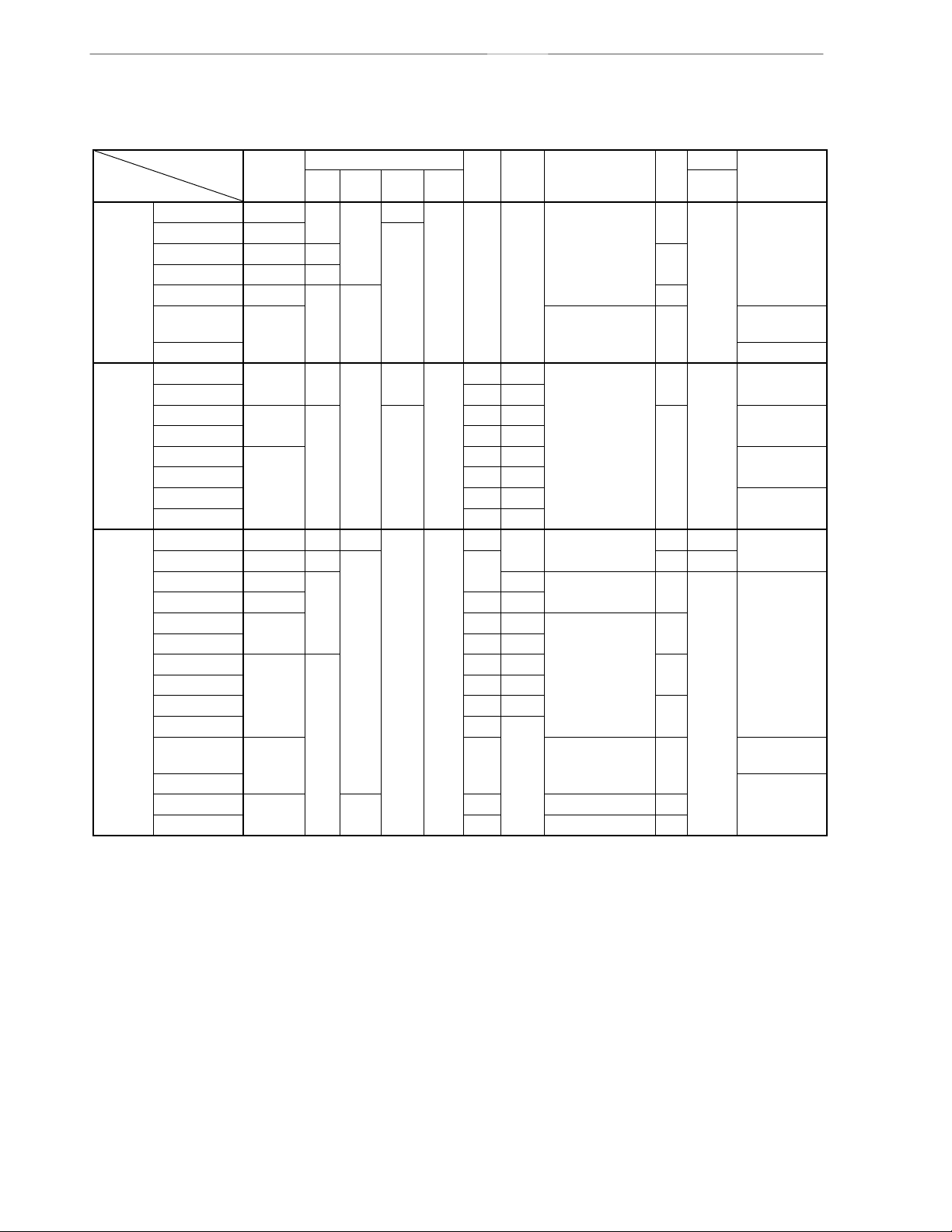
The products in the 78K/0S Series are listed below. The names enclosed in boxes are subseries names.
78K/0S
Series
44-pin
42-/44-pin
30-pin
30-pin
28-pin
20-pin
20-pin
44-pin
44-pin
30-pin
30-pin
30-pin
30-pin
30-pin
30-pin
144-pin
88-pin
80-pin
80-pin
80-pin
80-pin
64-pin
64-pin
64-pin
64-pin
64-pin
64-pin
52-pin
52-pin
Products in mass
production
Y subseries supports SMB.
Small-scale package, general-purpose applications
µ
µ
PD789046
PD789026
µ
µ
PD789088
µ
PD789074
µ
PD789014
µ
PD789062
µ
PD789052
Small-scale package, general-purpose applications and A/D function
PD789177Y
µ
PD789177
PD789167
µ
µ
PD789156
µ
PD789146
µ
PD789134A
µ
PD789124A
µ
PD789114A
PD789104A
µ
µ
µ
PD789167Y
PD789074 with subsystem clock added
PD789014 with enhanced timer function and expanded ROM and RAM
µ
PD789074 with enhanced timer function and expanded ROM and RAM
µ
PD789026 with enhanced timer function
µ
On-chip UART and capable of low-voltage (1.8 V) operation
RC oscillation version of PD789052
PD789860 without EEPROMTM, POC, and LVI
µ
PD789167 with 10-bit A/D
µ
µ
PD789104A with enhanced timer
PD789146 with 10-bit A/D
µ
PD789104A with EEPROM
µ
µ
PD789124A with 10-bit A/D
RC oscillation version of PD789104A
PD789104A with 10-bit A/D
µ
PD789026 with 8-bit A/D and multiplier added
µ
LCD drive
µ
PD789835
PD789830
µ
PD789489
µ
µ
PD789479
PD789417A
µ
µ
PD789407A
µ
PD789456
µ
PD789446
µ
PD789436
PD789426
µ
µ
PD789316
µ
PD789306
µ
PD789467
µ
PD789327
UART + 8-bit A/D + dot LCD (total display outputs: 96)
UART + dot LCD (40 × 16)
SIO + 10-bit A/D + internal voltage boosting method LCD (28 × 4)
SIO + 8-bit A/D + resistance division method LCD (28 × 4)
µ
PD789407A with 10-bit A/D
SIO + 8-bit A/D + resistance division method LCD (28 × 4)
PD789446 with 10-bit A/D
µ
SIO + 8-bit A/D + internal voltage boosting method LCD (15 × 4)
µ
PD789426 with 10-bit A/D
SIO + 8-bit A/D + internal voltage boosting method LCD (5 × 4)
RC oscillation version of PD789306
SIO + internal voltage boosting method LCD (24 × 4)
8-bit A/D + internal voltage boosting method LCD (23 × 4)
SIO + resistance division method LCD (24 × 4)
µ
µ
µ
Products under
development
TM
added
44-pin
44-pin
30-pin
30-pin
20-pin
20-pin
52-pin
64-pin
USB
µ
PD789800
Inverter control
µ
PD789842
On-chip bus controller
PD789850
µ
Keyless entry
µ
PD789862
PD789861
µ
PD789860
µ
VFD drive
µ
PD789871
Meter control
µ
PD789881
For PC keyboard. On-chip USB function
On-chip inverter controller and UART
On-chip CAN controller
PD789860 with enhanced timer function, SIO, and expanded ROM and RAM
µ
RC oscillation version of PD789860
On-chip POC and key return circuit
On-chip VFD controller (total display outputs: 25)
UART + resistance division method LCD (26 × 4)
Remark VFD (Vacuum Fluorescent Display) is referred to as FIP
documents, but the functions of the two are same.
User’s Manual U12978EJ3V0UD
µ
TM
(Fluorescent Indicator Panel) in some
23
Page 24
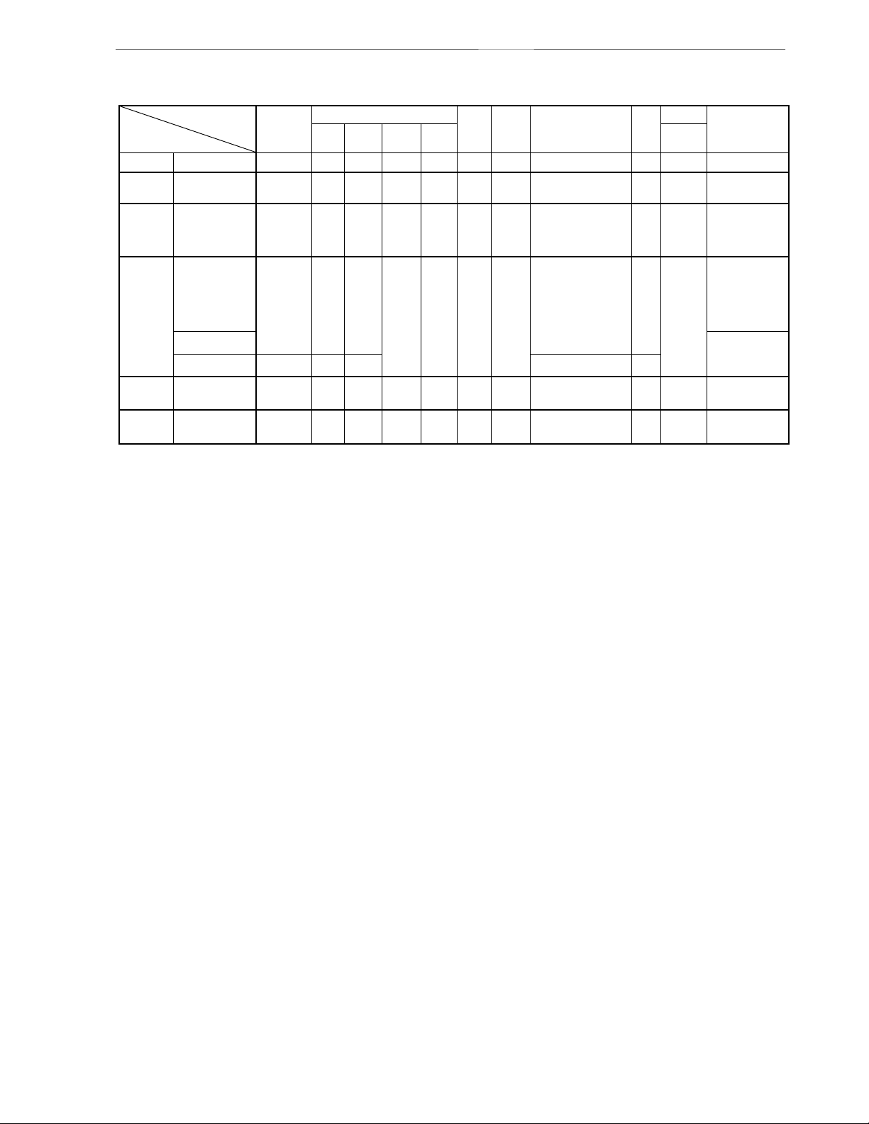
CHAPTER 1 GENERAL
The major differences between subseries are shown below.
Series for General-Purpose and LCD Drive
Subseries
Smallscale
package,
generalpurpose
applications
Smallscale
package,
generalpurpose
applications +
A/D
converter
LCD
drive
Function
PD789046 16 K 1 ch
µ
PD789026 4 K to 16 K
µ
PD789088
µ
PD789074 2 K to 8 K 1 ch
µ
PD789014 2 K to 4 K 2 ch
µ
PD789062 4 K
µ
PD789052
µ
PD789177
µ
PD789167
µ
PD789156
µ
PD789146
µ
PD789134A
µ
PD789124A 4 ch
µ
PD789114A
µ
PD789104A
µ
PD789835
µ
PD789830 24 K 1 ch
µ
PD789489
µ
PD789479
µ
PD789417A
µ
PD789407A
µ
PD789456
µ
PD789446 6 ch
µ
PD789436
µ
PD789426
µ
PD789316 RC-oscillation
µ
PD789306
µ
PD789467 1 ch
µ
PD789327
µ
ROM
Capacity
(Bytes)
16 K to 32 K
16 K to 24 K
8 K to 16 K
2 K to 8 K
24 K to 60 K
32 K to 48 K
24 K to 48 K
12 K to 24 K
12 K to 16 K
8 K to 16 K
4 K to 24 K
Note Flash memory version: 3.0 V
Timer V
8-Bit 16-Bit Watch WDT
1 ch
1 ch 34
−
3 ch
−
3 ch 1 ch
1 ch
−
−
−
1 ch 1 ch
1 ch
6 ch
1 ch
3 ch
2 ch
8-Bit
10-Bit
A/D
1 ch
−−
−
1ch
8 ch
8 ch
−
4 ch
4 ch
−
4 ch
−
4 ch
4 ch
3 ch 37 1.8 V
−
8 ch
8 ch
−
7 ch
7 ch
−
6 ch
−
6 ch
6 ch
−
−
Serial Interface I/O
A/D
1 ch (UART: 1ch)
1 ch (UART: 1ch)
−
−
−
−
−
1 ch (UART: 1ch)
2 ch (UART: 1ch) 45
−
1 ch (UART: 1ch) 43
−
−
−
2 ch (UART: 1ch) 23
1 ch 21
−
−
24
22
14 RC-oscillation
31
20
30 2.7 V
30
40
18
DD
MIN.Value
1.8 V
1.8 V
Note
1.8 V
Remarks
−
version
−
−
On-chip
EEPROM
RC-oscillation
version
−
Dot LCD
supported
−
version
−
24
User’s Manual U12978EJ3V0UD
Page 25
Series for ASSP
CHAPTER 1 GENERAL
Function
Subseries
ROM
Capacity
(Bytes)
USB
Inverter
control
On-chip
bus
controller
Keyless
PD789800 8 K 2 ch
µ
PD789842 8 K to 16 K 3 ch
µ
PD789850 16 K 1 ch 1 ch
µ
PD789861 1.8 V RC-oscillation
µ
4 K 2 ch
entry
PD789860
µ
PD789862 16 K 1 ch 2 ch 1 ch (UART: 1ch) 22
µ
VFD
PD789871 4 K to 8 K 3 ch
µ
drive
Meter
PD789881 16 K 2 ch 1 ch
µ
control
Notes 1. 10-bit timer: 1 channel
2. Flash memory version: 3.0 V
Timer V
8-Bit 16-Bit Watch WDT
−−
Note 1
−−
−
1 ch
1 ch 1 ch 8 ch
−
1 ch 4 ch
1 ch
1 ch 1 ch
−
1 ch
8-Bit
10-Bit
A/D
−−
Serial Interface I/O
A/D
2 ch (USB: 1ch) 31 4.0 V
−
1 ch (UART: 1ch) 30 4.0 V
−
2 ch (UART: 1ch) 18 4.0 V
−− −
−−
−−
1 ch 33 2.7 V
1 ch (UART: 1 ch) 28 2.7 V
14
DD
MIN.Value
Note 2
Remarks
−
−
−
version,
on-chip
EEPROM
On-chip
EEPROM
−
−
User’s Manual U12978EJ3V0UD
25
Page 26
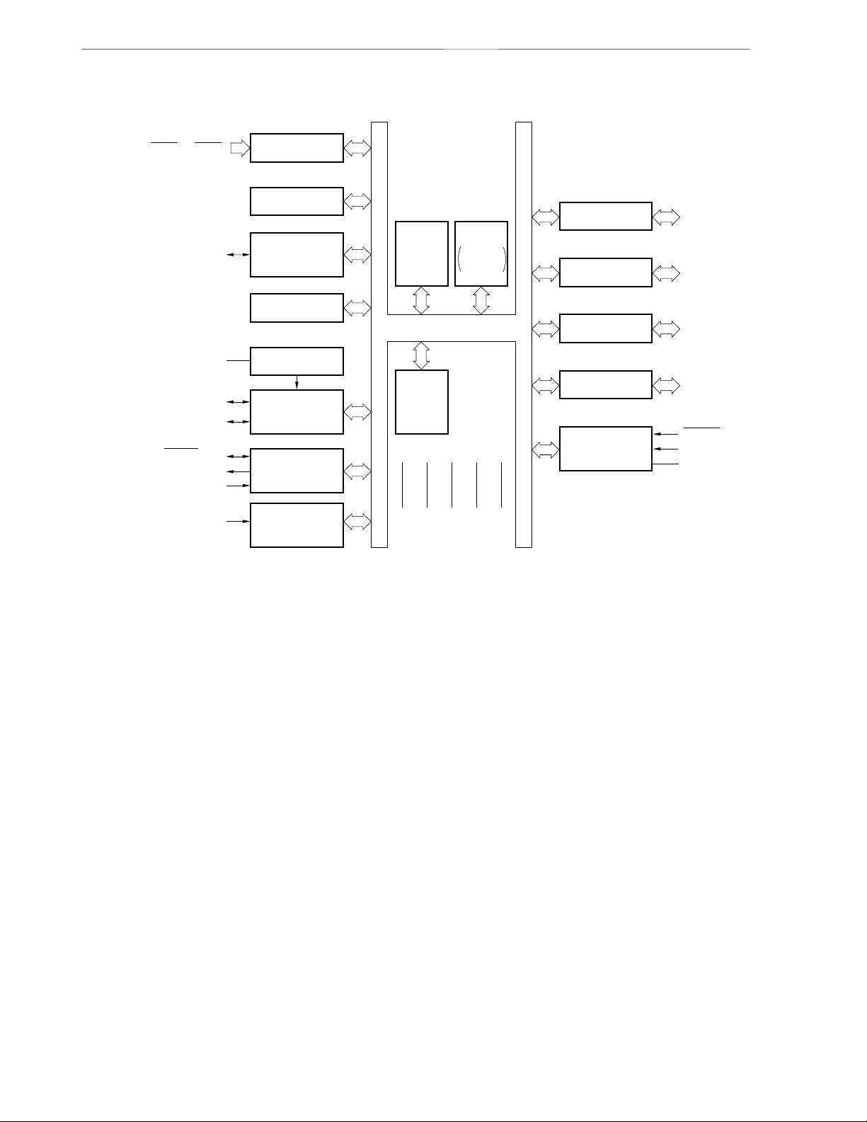
1.6 Block Diagram
CHAPTER 1 GENERAL
KR00 to KR07
TI01/TO01/P26/INTP0
REGC
USBDM
USBDP
SCK10/P20
SO10/P21
SI10/P22
INTP0/P26
Key return 0
8-bit timer 00
8-bit timer/event
counter 01
Watchdog timer
Regulator
V
REG
USB
function 0
Serial
interface 1
Interrupt
control
78K/0S
CPU
core
RAM
V
DD0VDD1VSS0VSS1
ROM
Flash
memory
IC
(VPP)
Port 0
Port 1
Port 2
Port 4
System control
P00 to P07
P10 to P17
P20 to P26
P40 to P47
RESET
X1
X2
Remark The parenthesized values apply to the
PD78F9801.
µ
26
User’s Manual U12978EJ3V0UD
Page 27
1.7 Functions
CHAPTER 1 GENERAL
Product
PD789800
µ
Item
Internal memory ROM Mask ROM
8 KB
Flash memory
16 KB
High-speed RAM 256 bytes
Minimum instruction execution time 0.33 µs/1.33 µs (at 6.0 MHz operation with system clock)
Instruction set • 16-bit operation
• Bit manipulation (set, reset, and test) etc.
I/O ports CMOS I/O 31
(Of the above COMS I/O ports, 18 ports can be switched to N-ch open-drain
I/O ports.)
Serial interface • USB (Universal Serial Bus) function: 1 channel
• Three-wired serial I/O mode: 1 channel
Timer • 8-bit timer: 1 channel
• 8-bit timer/event counter: 1 channel
• Watchdog timer: 1 channel
Regulator Incorporated (V
Vector interrupt
sources
Maskable
Non-maskable Internal: 1
Internal: 9, external: 2
= 3.3 ±0.3 V)
REG
Power supply voltage VDD = 4.0 to 5.5 V
Operating ambient temperature • TA = –40 to +85°C (when the USB is not operating)
•T
= 0 to +70°C (when the USB is operating)
A
•T
= 10 to 40°C (when a flash memory is written)
A
Package 44-pin plastic LQFP (10 × 10)
PD78F9801
µ
An outline of the timer is shown below.
Operation mode
Function
8-Bit Timer 00 8-Bit Timer/
Event Counter 01
Interval timer 1 channel 1 channel 1 channel
External event counter −−−− 1 channel −−−−
Timer outputs −−−− 1 output −−−−
Square-wave outputs −−−− 1 output −−−−
Capture −−−−−
−−
−−
Interrupt sources 1 1 2
Watchdog Timer
Note
−
−−
Note The watchdog timer has watchdog timer and interval timer functions. However, use the watchdog timer by
selecting either the watchdog timer function or interval timer function.
User’s Manual U12978EJ3V0UD
27
Page 28
CHAPTER 2 PIN FUNCTIONS
2.1 List of Pin Functions
(1) Port pins
Pin Name I/O Function After Reset Alternate
Function
P00 to P07 I/O Port 0
8-bit I/O port
Input/output can be specified in 1-bit units.
When used as an input port, use of on-chip pull-up resistors can be
specified by pull-up resistor option register 0 (PU0).
When used as an output port, CMOS output or N-ch open-drain
output can be specified in 8-bit units by port output mode register 0
(POM0).
P10 to P17 I/O Port 1
8-bit I/O port
Input/output can be specified in 1-bit units.
When used as an input port, use of on-chip pull-up resistors can be
specified by pull-up resistor option register 0 (PU0).
When used as an output port, CMOS output or N-ch open-drain
output can be specified in 8-bit units by port output mode register 0
(POM0).
P20
P21 SO10
P22 SI10
P23 to P25 —
P26
P40 to P47 I/O Port 4
I/O Port 2
7-bit I/O port
Input/output can be specified in 1-bit units.
When used as an input port, use of on-chip pull-up resistors can be
specified by pull-up resistor option register 0 (PU0).
When P25 or P26 is used as an output port, CMOS output or N-ch
open-drain output can be specified in 1-bit units by port output mode
register 1 (POM1).
8-bit I/O port
Input/output can be specified in 1-bit units.
When used as an input port, use of on-chip pull-up resistors can be
specified by pull-up resistor option register 0 (PU0).
Input —
Input —
Input
Input
SCK10
INTP0/TI01/TO01
KR00 to KR07
28
User’s Manual U12978EJ3V0UD
Page 29
CHAPTER 2 PIN FUNCTIONS
(2) Non-port pins
Pin Name I/O Function After Reset Alternate
Function
INTP0 Input External interrupt request input for which valid edge (rising
and/or falling edge) can be specified
KR00 to
Input Input for detecting key return signals Input P40 to P47
KR07
NC — No connection. Can be left open. — —
REGC — Internally generated power supply for driving USB
RESET
SCK10
driver/receiver. Connect this pin to V
Input System reset input Input —
I/O Serial clock input/output for serial interface Input P20
via a 22 µF capacitor.
SS
SI10 Input Serial data input for serial interface Input P22
SO10 Output Serial data output for serial interface Input P21
TI01 Input External count clock input to 8-bit timer TM01 Input P26/INTP0/TO01
TO01 Output Output from 8-bit timer TM01 Input P26/INTP0/TI01
USBDM I/O Serial data input/output (negative side) for USB function. The
pull-up resistor (1.5 kΩ) for the USBDM pin must be
connected to the REGC pin.
USBDP I/O Serial data input/output (positive side) for USB function Input —
V
DD0
V
DD1
V
SS0
V
SS1
X1 Input Input —
— Positive power supply for ports — —
— Positive power supply for circuits other than ports — —
— Ground potential for ports — —
— Ground potential for circuits other than ports — —
Crystal resonator connection to for system clock oscillator
X2 —
IC — Internally connected directly to V
V
PP
— Sets flash memory programming mode. Apply high voltage
SS0
when a program is written or verified.
Input P26/TI01/TO01
——
Input —
——
——
——
User’s Manual U12978EJ3V0UD
29
Page 30

CHAPTER 2 PIN FUNCTIONS
2.2 Pin Functions
2.2.1 P00 to P07 (Port 0)
These pins constitute an 8-bit I/O port and can be set to the input or output port mode in 1-bit units by using port
mode register 0 (PM0). When these pins are used as an input port, an on-chip pull-up resistor can be used by
setting pull-up resistor option register 0 (PU0). When these pins are used as an output port, CMOS output or N-ch
open-drain output can be specified in 8-bit units by setting port output mode register 0 (POM0).
2.2.2 P10 to P17 (Port 1)
These pins constitute an 8-bit I/O port. Port 1 can be set to the input or output mode in 1-bit units by using port
mode register 1 (PM1). When the port is used as an input port, an on-chip pull-up resistor can be used by setting
pull-up resistor option register 0 (PU0). When these pins are used as an output port, CMOS output or N-ch open-
drain output can be specified in 8-bit units by setting port output mode register 0 (POM0).
2.2.3 P20 to P26 (Port 2)
These pins constitute a 7-bit I/O port. In addition, these pins function as data I/O, and clock I/O to and from the
serial interface, external interrupt input, and timer I/O.
Port 2 can be specified in the following operation modes in 1-bit units.
(1) Port mode
In the port mode, P20 to P26 function as a 7-bit I/O port. Port 2 can be set to the input or output mode in 1-bit
units by using port mode register 2 (PM2). When the port is used as an input port, an on-chip pull-up resistor
can be used by setting pull-up resistor option register 0 (PU0). When P25 or P26 is used as an output port,
CMOS output or N-ch open-drain output can be specified by setting in 1-bit units port output mode register 1
(POM1).
(2) Control mode
In this mode, P20 to P26 function as the data I/O and the clock I/O to and from the serial interface.
(a) SI10, SO10
These are the serial data I/O pins of the serial interface.
(b) SCK10
This is the serial clock I/O pin of the serial interface.
(c) TI01
This is the external clock input pin for the 8-bit timer/event counter.
(d) TO01
This is the output pin of the 8-bit timer.
(e) INTP0
This is an external interrupt input pin for which the valid edge (rising edge, falling edge, or both rising and
falling edges) can be specified.
Caution When using P20 to P26 as serial interface pins, the I/O mode and output latch must be set
according to the functions to be used. For setting details, see Table 9-2.
30
User’s Manual U12978EJ3V0UD
Page 31

CHAPTER 2 PIN FUNCTIONS
2.2.4 P40 to P47 (Port 4)
These pins constitute an 8-bit I/O port. In addition, they also function as key return signal detection pins.
The following operation modes can be specified in 1-bit units.
(1) Port mode
In this mode, port 4 functions as an 8-bit I/O port. Port 4 can be set to the input or output mode in 1-bit units by
using port mode register 4 (PM4). When used as an input port an on-chip pull-up resistor can be used by
setting pull-up resistor option register 0 (PU0).
(2) Control mode
In this mode, the pins function as key return signal detection pins (KR00 to KR07).
2.2.5 RESET
This pin inputs an active-low system reset signal.
2.2.6 X1, X2
These pins are used to connect a crystal resonator for system clock oscillation.
To supply an external clock, input the clock to X1 and input the inverted signal to X2.
2.2.7 REGC
This pin is a power supply pin for driving a USB driver/receiver generated internally. Connect this pin to the VSS
pin via 22 µF capacitor.
2.2.8 USBDM
This pin (negative side) inputs or outputs serial data for the USB function.
2.2.9 USBDP
This pin (positive side) inputs or outputs serial data for the USB function.
2.2.10 V
DD0, VDD1
These pins are positive power supply pins.
2.2.11 V
SS0, VSS1
These pins are ground pins.
User’s Manual U12978EJ3V0UD
31
Page 32

CHAPTER 2 PIN FUNCTIONS
2.2.12 VPP (
µµµµ
PD78F9801 only)
A high voltage should be applied to this pin when the flash memory programming mode is set and when the
program is written or verified.
Handle this pin in either of the following ways.
• Independently connect a 10 kΩ pull-down resistor.
• Switch this pin to be directly connected to the dedicated flash programmer in programming mode or to VSS0
normal operation mode using a jumper on the board.
2.2.13 IC (mask ROM version only)
The IC (Internally Connected) pin is used to set the µPD789800 Subseries in the test mode before shipment. In
the normal operation mode, directly connect this pin to the V
If a potential difference is generated between the IC pin and V
pin and V
pin or an external noise superimposed on the IC pin, a user program may not run correctly.
SS0
• Directly connect the IC pin to the V
V
pin with as short a wiring length as possible.
SS0
pin due to a long wiring length between the IC
SS0
pin.
SS0
IC
SS0
Keep short
in
32
User’s Manual U12978EJ3V0UD
Page 33

CHAPTER 2 PIN FUNCTIONS
2.3 Pin I/O Circuits and Recommended Connection of Unused Pins
Table 2-1 lists the types of I/O circuits for each pin and explains how unused pins are handled.
Figure 2-1 shows the configuration of each type of I/O circuit.
Table 2-1. Type of Pin I/O Circuit Recommended Connection of Unused Pins
Pin Name I/O Circuit Type I/O Recommended Connection of Unused Pins
P00 to P07
P10 to P17
P20/
SCK10
P21/SO10
P22/SI10
P23, P24
P25
P26/INTP0/TI01/TO01
P40/
KR00 to
P47/
KR07
5-R
8-C
8-F
8-C
I/O
Input: Independently connect to V
resistor.
Output: Leave open.
DD0
, V
DD1
, V
SS0
, or V
SS1
via a
USBDM Connect to the REGC pin.
USBDP
RESET
24-A
Independently connect to V
2 Input —
NC ——Leave open.
REGC ——Connect to USBDM pin.
IC Connect directly to V
V
PP
——
Independently connect a 10 kΩ pull-down resistor, or connect directly
to V
SS0
.
SS0
.
SS0
or V
via a resistor.
SS1
User’s Manual U12978EJ3V0UD
33
Page 34

CHAPTER 2 PIN FUNCTIONS
Figure 2-1. Pin I/O Circuits
Type 2
IN
Schmitt-triggered input with hysteresis characteristics
Type 5-R
Pull-up
enable
P-ch
cut
Output
data
Output
VDD0
P-ch
N-ch
DD0
V
P-ch
disable
VSS0
IN/OUT
Type 8-F
Pull-up
enable
P-ch
cut
Output
data
Output
disable
Type 24-A
TXDXP
RXDX
TXDXN
VSS0
VDD0
V
VSS0
P-ch
N-ch
REG
P-ch
N-ch
V
DD0
P-ch
IN/OUT
IN/OUT
34
Input
enable
Type 8-C
Pull-up
enable
Output
data
Output
disable
VDD0
P-ch
DD0
V
P-ch
IN/OUT
N-ch
SS0
V
User’s Manual U12978EJ3V0UD
Page 35

CHAPTER 3 CPU ARCHITECTURE
3.1 Memory Space
The µPD789800 Subseries can access 64 KB of memory space.
Figures 3-1 and 3-2 show the memory maps.
Data memory
space
Figure 3-1. Memory Map (
HFFFF
Special function register
256 × 8 bits
H00FF
HFFEF
Internal high-speed RAM
256 × 8 bits
H00EF
HFFDF
Reserved
H0002
HFFF1
µµµµ
PD789800)
HFFF1
Program area
Program memory
space
Internal ROM
8,192 × 8 bits
H0000
User’s Manual U12978EJ3V0UD
H0800
HF700
CALLT table area
H0400
HF300
Program area
HA100
H9100
Vector table area
H0000
35
Page 36

CHAPTER 3 CPU ARCHITECTURE
Data memory
space
Figure 3-2. Memory Map (
HFFFF
Special function register
256 × 8 bits
H00FF
HFFEF
Internal high-speed RAM
256 × 8 bits
H00EF
HFFDF
Reserved
H0004
HFFF3
µµµµ
PD78F9801)
HFFF3
Program area
Program memory
space
Flash memory
16,384 × 8 bits
H0000
H0800
HF700
CALLT table area
H0400
HF300
Program area
HA100
H9100
Vector table area
H0000
36
User’s Manual U12978EJ3V0UD
Page 37

CHAPTER 3 CPU ARCHITECTURE
3.1.1 Internal program memory space
The internal program memory space stores programs and table data. This space is usually addressed by the
program counter (PC).
The following areas are allocated to the internal program memory space.
(1) Vector table area
A 26-byte area of addresses 0000H to 0019H is reserved as a vector table area. This area stores program start
addresses to be used when branching by RESET input or interrupt request generation. Of a 16-bit program
address, the lower 8 bits are stored in an even address, and the higher 8 bits are stored in an odd address.
Table 3-1. Vector Table
Vector Table Address Interrupt Request Vector Table Address Interrupt Request
0000H RESET input 000EH INTUSBRE
0004H INTWDT 0010H INTP0
0006H INTUSBTM 0012H INTCSI10
0008H INTUSBRT 0014H INTTM00
000AH INTUSBRD 0016H INTTM01
000CH INTUSBST 0018H INTKR00
(2) CALLT instruction table area
The subroutine entry address of a 1-byte call instruction (CALLT) can be stored in a 64-byte area of addresses
0040H to 007FH.
3.1.2 Internal data memory (internal high-speed RAM) space
An internal high-speed RAM is incorporated in the area between FE00H and FEFFH.
The internal high-speed RAM is also used as a stack.
3.1.3 Special function register (SFR) area
Special function registers (SFRs) of on-chip peripheral hardware are allocated to an area of FF00H to FFFFH
(see Table 3-2).
User’s Manual U12978EJ3V0UD
37
Page 38

CHAPTER 3 CPU ARCHITECTURE
3.1.4 Data memory addressing
PD789800 Subseries provides a variety of addressing modes which take account of memory manipulability,
The
µ
etc. Especially at addresses corresponding to data memory area (FE00H to FFFFH), particular addressing modes
are possible to meet the functions of the special function registers (SFR) and general-purpose registers. Figures 3-3
and 3-4 show the data memory addressing modes.
FFFFH
FF20H
FF1FH
FF00H
FEFFH
FE20H
FE1FH
FE00H
FDFFH
Figure 3-3. Data Memory Addressing (
Special function registers (SFR)
256 × 8 bits
Internal high-speed RAM
256 × 8 bits
Reserved
SFR addressing
µµµµ
PD789800)
Short direct
addressing
Direct addressing
Register indirect
addressing
Based addressing
38
2000H
1FFFH
Internal ROM
8,192 × 8 bits
0000H
User’s Manual U12978EJ3V0UD
Page 39

CHAPTER 3 CPU ARCHITECTURE
FFFFH
FF20H
FF1FH
FF00H
FEFFH
FE20H
FE1FH
FE00H
FDFFH
Figure 3-4. Data Memory Addressing (
Special function registers (SFR)
256 × 8 bits
Internal high-speed RAM
256 × 8 bits
Reserved
SFR addressing
µµµµ
PD78F9801)
Short direct
addressing
Direct addressing
Register indirect
addressing
Based addressing
4000H
3FFFH
0000H
Flash memory
16,384 × 8 bits
User’s Manual U12978EJ3V0UD
39
Page 40

CHAPTER 3 CPU ARCHITECTURE
3.2 Processor Registers
The µPD789800 Subseries provides the following on-chip processor registers.
3.2.1 Control registers
The control registers contain special functions to control the program sequence, statuses and stack memory. A
program counter, a program status word, and a stack pointer are the control registers.
(1) Program counter (PC)
The program counter is a 16-bit register which holds the address information of the next program to be
executed.
In normal operation, the PC is automatically incremented according to the number of bytes of the instruction to
be fetched. When a branch instruction is executed, immediate data or register contents are set.
RESET input sets the program counter to the reset vector table values at addresses 0000H and 0001H.
Figure 3-5. Configuration of Program Counter
15 0
PC15PC PC14 PC13 PC12 PC11 PC10 PC9 PC8 PC7 PC6 PC5 PC4 PC3 PC2 PC1 PC0
(2) Program status word (PSW)
The program status word is an 8-bit register consisting of various flags to be set/reset by instruction execution.
Program status word contents are automatically stacked upon interrupt request generation or PUSH PSW
instruction execution and are automatically restored upon execution of the RETI and POP PSW instructions.
RESET input sets the PSW to 02H.
Figure 3-6. Configuration of Program Status Word
70
IE
Z 0 AC 0 0 1 CY
40
User’s Manual U12978EJ3V0UD
Page 41

CHAPTER 3 CPU ARCHITECTURE
(a) Interrupt enable flag (IE)
This flag controls interrupt request acknowledgment operations of the CPU.
When 0, the IE flag is set to the interrupt disabled status (DI), and interrupt requests other than non-
maskable interrupts are all disabled.
When 1, the IE flag is set to the interrupt enabled status (EI). Interrupt request acknowledgment enable is
controlled by the interrupt mask flag corresponding to each interrupt source.
The IE flag is reset (0) upon DI instruction execution or interrupt acknowledgment and is set (1) upon EI
instruction execution.
(b) Zero flag (Z)
When the operation result is zero, this flag is set (1). It is reset (0) in all other cases.
(c) Auxiliary carry flag (AC)
If the operation result has a carry from bit 3 or a borrow at bit 3, this flag is set (1). It is reset (0) in all other
cases.
(d) Carry flag (CY)
This flag stores overflow and underflow upon add/subtract instruction execution. It stores the shift-out
value upon rotate instruction execution and functions as a bit accumulator during bit manipulation
instruction execution.
User’s Manual U12978EJ3V0UD
41
Page 42

CHAPTER 3 CPU ARCHITECTURE
(3) Stack pointer (SP)
This is a 16-bit register that holds the start address of the memory stack area. Only the internal high-speed
RAM area can be set as the stack area.
Figure 3-7. Configuration of Stack Pointer
15 0
SP15SP SP14 SP13 SP12 SP11 SP10 SP9 SP8 SP7 SP6 SP5 SP4 SP3 SP2 SP1 SP0
The SP is decremented ahead of write (save) to the stack memory and is incremented after read (restore) from
the stack memory.
Each stack operation saves/restores data as shown in Figures 3-8 and 3-9.
Caution Since RESET input makes the SP contents undefined, be sure to initialize the SP before
instruction execution.
Figure 3-8. Data to Be Saved to Stack Memory
SP SP _ 2
SP _ 2
SP _ 1
SP
SP
SP + 1
PUSH rp
instruction
Lower half
register pairs
Upper half
register pairs
SP SP _ 2
SP _ 2
SP _ 1
SP
CALL, CALLT
instructions
PC7 to PC0
PC15 to PC8
Figure 3-9. Data to Be Restored from Stack Memory
instruction
Lower half
register pairs
Upper half
register pairs
SP
SP + 1
RET instructionPOP rp
PC7 to PC0
PC15 to PC8
SP SP _ 3
SP _ 3
SP _ 2
SP _ 1
SP
SP
SP + 1
Interrupt
PC7 to PC0
PC15 to PC8
PSW
RETI instruction
PC7 to PC0
PC15 to PC8
42
SP SP + 2
SP SP + 2
User’s Manual U12978EJ3V0UD
SP + 2
SP SP + 3
PSW
Page 43

CHAPTER 3 CPU ARCHITECTURE
3.2.2 General-purpose registers
The general-purpose registers consist of eight 8-bit registers (X, A, C, B, E, D, L, and H).
In addition that each register can be used as an 8-bit register, two 8-bit registers in pairs can be used as a 16-bit
register (AX, BC, DE, and HL).
They can be described in terms of functional names (X, A, C, B, E, D, L, H, AX, BC, DE, and HL) and absolute
names (R0 to R7 and RP0 to RP3).
Figure 3-10. Configuration of General-Purpose Registers
(a) Absolute names
16-bit processing 8-bit processing
R7
RP3
R6
R5
RP2
R4
R3
RP1
R2
R1
RP0
R0
15 0 7 0
(b) Functional names
16-bit processing 8-bit processing
H
HL
L
D
DE
BC
AX
E
B
C
A
X
15 0 7 0
User’s Manual U12978EJ3V0UD
43
Page 44

CHAPTER 3 CPU ARCHITECTURE
3.2.3 Special function registers (SFRs)
Unlike general-purpose registers, each special function register has a special function.
The special function registers are allocated in the 256-byte area FF00H to FFFFH.
The special function registers can be manipulated, like the general-purpose registers, with operation, transfer, and
bit manipulation instructions. Manipulatable bit units (1, 8, and 16) differ depending on the special function register
type.
Each manipulation bit can be specified as follows.
• 1-bit manipulation
Describe the symbol reserved by the assembler for the 1-bit manipulation instruction operand (sfr.bit). This
manipulation can also be specified using address.
• 8-bit manipulation
Describe the symbol reserved by the assembler for the 8-bit manipulation instruction operand (sfr). This
manipulation can also be specified using an address.
• 16-bit manipulation
Describe the symbol reserved by the assembler for the 16-bit manipulation instruction operand. When
specifying an address, describe an even address.
Table 3-2 lists the special function registers. The meanings of the symbols in this table are as follows.
• Symbol
Indicates the address of the implemented special function register. The symbols shown in this column are
reserved words in the assembler, and have already been defined in the header file “sfrbit.h” in the C compiler.
Therefore, these symbols can be used as instruction operands if an assembler or integrated debugger is used.
• R/W
Indicates whether the special function register in question can be read or written.
R/W: Read/write
R: Read only
W: Write only
• Bit units for manipulation
Indicates the bit units (1, 8, 16) in which the special function register in question can be manipulated.
• After reset
Indicates the status of the special function register when the RESET signal is input.
44
User’s Manual U12978EJ3V0UD
Page 45

CHAPTER 3 CPU ARCHITECTURE
Table 3-2. Special Function Register List (1/3)
Address Special Function Register (SFR) Name Symbol R/W Manipulatable Bit Unit After Reset
1 Bit 8 Bits 16 Bits
FF00H Port 0 P0 R/W √√— 00H
FF01H Port 1 P1 √√—
FF02H Port 2 P2 √√—
FF04H Port 4 P4 √√—
FF07H Receive data PID USBRD R — √ —
FF08H Receive data address 0
FF09H Receive data address 1
FF0AH Receive data address 2
FF0BH Receive data address 3
FF0CH Receive data address 4
FF0DH Receive data address 5
FF0EH Receive data address 6
FF0FH Receive data address 7
USBR0 USBR10
USBR1
USBR2 USBR32
USBR3
USBR4 USBR54
USBR5
USBR6 USBR76
USBR7
— √√Undefined
— √
— √√
— √
— √√
— √
— √√
— √
FF10H Transmit/receive shift register 10 SIO10 R/W — √ —
FF14H Handshake packet transmit reservation
register
FF15H Data packet transmit reservation register DTX
HTX
RSV
USB
CON
√√ √00H
√√
RSV
FF20H Port mode register 0 PM0 √√— FFH
FF21H Port mode register 1 PM1 √√—
FF22H Port mode register 2 PM2 √√—
FF24H Port mode register 4 PM4 √√—
FF30H Port output mode register 0 POM0 √√— 00H
FF31H Port output mode register 1 POM1 √√—
FF42H Timer clock select register 2 TCL2 — √ —
FF50H 8-bit compare register 00 CR00 W — √ — Undefined
FF51H 8-bit timer counter 00 TM00 R — √ — 00H
FF53H 8-bit timer mode control register 00 TMC00 R/W √√—
FF54H 8-bit compare register 01 CR01 W — √ — Undefined
FF55H 8-bit timer counter 01 TM01 R — √ — 00H
FF57H 8-bit timer mode control register 01 TMC01 R/W √√—
FF60H Token PID compare register TIDCMP W — √ —
FF61H Token address compare register ADRCMP — √ —
Note
Note
Note
Note
Note
Note 16-bit access is possible only in short direct addressing.
User’s Manual U12978EJ3V0UD
45
Page 46

CHAPTER 3 CPU ARCHITECTURE
Table 3-2. Special Function Register List (2/3)
Address Special Function Register (SFR) Name Symbol R/W Manipulatable Bit Unit After Reset
1 Bit 8 Bits 16 Bits
FF62H Token packet receive result store register TRXRSL R/W √√— 00H
FF63H Data/handshake PID compare register DIDCMP W — √ — C3H
FF64H Data/handshake packet receive byte
number counter
FF65H Data/handshake packet receive result store
register
FF66H Data/handshake packet receive mode
register
FF67H Packet receive status register RXSTAT — √ —
FF68H Data packet transmit byte number counter 0 DTXCO0 W — √ — 20H
FF69H Data packet transmit byte number counter 1 DTXCO1 — √ — 30H
FF6AH Remote wakeup control register REMWUP R/W √√— 08H
FF6BH Transmit/receive pointer USBPOW R — √ — 00H
FF6CH USB timer start reservation control register USBTCL R/W √√— 01H
FF6DH USB receiver enable register USBMOD √√— 00H
FF72H Serial operation mode register 10 CSIM10 √√—
FFA1H Transmit data PID bank 0 USBTD0 W — √ — Undefined
FFA2H Transmit data bank 0 address 00 USBT00 — √ —
FFA3H Transmit data bank 0 address 01 USBT01 — √ —
FFA4H Transmit data bank 0 address 02 USBT02 — √ —
FFA5H Transmit data bank 0 address 03 USBT03 — √ —
FFA6H Transmit data bank 0 address 04 USBT04 — √ —
FFA7H Transmit data bank 0 address 05 USBT05 — √ —
FFA8H Transmit data bank 0 address 06 USBT06 — √ —
FFA9H Transmit data bank 0 address 07 USBT07 — √ —
FFABH Transmit data PID bank 1 USBTD1 — √ —
FFACH Transmit data bank 1 address 10 USBT10 — √ —
FFADH Transmit data bank 1 address 11 USBT11 — √ —
FFAEH Transmit data bank 1 address 12 USBT12 — √ —
FFAFH Transmit data bank 1 address 13 USBT13 — √ —
FFB0H Transmit data bank 1 address 14 USBT14 — √ —
FFB1H Transmit data bank 1 address 15 USBT15 — √ —
FFB2H Transmit data bank 1 address 16 USBT16 — √ —
FFB3H Transmit data bank 1 address 17 USBT17 — √ —
FFB5H Receive token PID USBRTP R — √ — 00H
FFB6H Receive token address L USBRAL — √ —
FFB7H Receive token address H USBRAH — √ —
FFE0H Interrupt request flag register 0 IF0 R/W √√—
FFE1H Interrupt request flag register 1 IF1 √√—
FFE4H Interrupt mask flag register 0 MK0 √√— FFH
FFE5H Interrupt mask flag register 1 MK1 √√—
DRXCON — √ — 18H
DRXRSL R/W √√— 00H
URXMOD √√—
46
User’s Manual U12978EJ3V0UD
Page 47

CHAPTER 3 CPU ARCHITECTURE
Table 3-2. Special Function Register List (3/3)
Address Special Function Register (SFR) Name Symbol R/W Manipulatable Bit Unit After Reset
1 Bit 8 Bits 16 Bits
FFECH External interrupt mode register 0 INTM0 R/W — √ — 00H
FFF5H Key return mode register 00 KRM00 √√—
FFF7H Pull-up resistor option register 0 PU0 √√—
FFF9H Watchdog timer mode register WDTM √√—
FFFAH Oscillation stabilization time select register OSTS — √ — 04H
FFFBH Processor clock control register PCC √√— 02H
User’s Manual U12978EJ3V0UD
47
Page 48

CHAPTER 3 CPU ARCHITECTURE
3.3 Instruction Address Addressing
An instruction address is determined by program counter (PC) contents. PC contents are normally incremented
(+1 for each byte) automatically according to the number of bytes of an instruction to be fetched each time another
instruction is executed. When a branch instruction is executed, the branch destination information is set to the PC
and branched by the following addressing (for details of each instruction, refer to 78K/0S Series Instruction User’s
Manual (U11047E)).
3.3.1 Relative addressing
[Function]
The value obtained by adding 8-bit immediate data (displacement value: jdisp8) of an instruction code to the
start address of the following instruction is transferred to the program counter (PC) and branched. The
displacement value is treated as signed two’s complement data (−128 to +127) and bit 7 becomes a sign bit.
This means that information is relatively branched to a location between −128 and +127, from the start address
of the next instruction when relative addressing is used.
This function is carried out when the BR $addr16 instruction or a conditional branch instruction is executed.
[Illustration]
15 0
PC
+
15 0
α
15 0
PC
When S = 0, α indicates all bits 0.
When S = 1, α indicates all bits 1.
876
S
jdisp8
...
PC is the start address of
the next instruction of
a BR instruction.
48
User’s Manual U12978EJ3V0UD
Page 49

CHAPTER 3 CPU ARCHITECTURE
3.3.2 Immediate addressing
[Function]
Immediate data in the instruction word is transferred to the program counter (PC) and branched.
This function is carried out when the CALL !addr16 or BR !addr16 instruction is executed.
The CALL !addr16 and BR !addr16 instructions can be branched to any location in the memory space.
[Illustration]
In case of CALL !addr16 and BR !addr16 instructions
70
CALL or BR
Low Addr.
High Addr.
15 0
PC
87
User’s Manual U12978EJ3V0UD
49
Page 50

CHAPTER 3 CPU ARCHITECTURE
3.3.3 Table indirect addressing
[Function]
Table contents (branch destination address) of the particular location to be addressed by the lower-5-bit
immediate data of an instruction code from bit 1 to bit 5 are transferred to the program counter (PC) and
branched.
This function is carried out when the CALLT [addr5] instruction is executed. The instruction enables a branch
to any location in the memory space by referring to the addresses stored in the memory table at 40H to 7FH.
[Illustration]
765 10
Instruction code
ta4–0
001
Effective address
Effective address + 1
15 1
0100000000
Memory (Table)
70
Low Addr.
High Addr.
15 0
PC
87
87
65 0
0
3.3.4 Register addressing
[Function]
Register pair (AX) contents to be specified with an instruction word are transferred to the program counter
(PC) and branched.
This function is carried out when the BR AX instruction is executed.
[Illustration]
50
70
rp
15 0
PC
AX
User’s Manual U12978EJ3V0UD
07
87
Page 51

CHAPTER 3 CPU ARCHITECTURE
3.4 Operand Address Addressing
The following methods are available to specify the register and memory (addressing) to undergo manipulation
during instruction execution.
3.4.1 Direct addressing
[Function]
The memory indicated by immediate data in an instruction word is directly addressed.
[Operand format]
Identifier Description
addr16 Label or 16-bit immediate data
[Description example]
MOV A, !FE00H; When setting !addr16 to FE00H
Instruction code 00101001Opcode
[Illustration]
00000000
11111110
70
Opcode
addr16 (Low)
addr16 (High)
00H
FEH
Memory
User’s Manual U12978EJ3V0UD
51
Page 52

CHAPTER 3 CPU ARCHITECTURE
3.4.2 Short direct addressing
[Function]
The memory to be manipulated in the fixed space is directly addressed with 8-bit data in an instruction word.
The fixed space is the 256-byte space FE20H to FF1FH where the addressing is applied. An internal high-
speed RAM and special function registers (SFR) are mapped at FE20H to FEFFH and FF00H to FF1FH,
respectively.
The SFR area (FF00H to FF1FH), where short direct addressing is applied, is a part of the whole SFR area.
In this area, ports which are frequently accessed in a program and a compare register of the timer/event
counter are mapped, and these SFRs can be manipulated with a small number of bytes and clocks.
When 8-bit immediate data is at 20H to FFH, bit 8 of an effective address is set to 0. When it is at 00H to
1FH, bit 8 is set to 1. See [Illustration] below.
[Operand format]
Identifier Description
saddr Label or FE20H to FF1FH immediate data
saddrp Label or FE20H to FF1FH immediate data (even address only)
[Description example]
MOV FE30H, #50H; When setting saddr to FE30H and the immediate data to 50H
Instruction code 1 1 1 1 0 1 0 1
00110000
01010000
Opcode
30H (saddr-offset)
50H (Immediate data)
[Illustration]
07
Opcode
saddr-offset
8
α
0
Effective
address
15
1
111111
Short direct memory
52
When 8-bit immediate data is 20H to FFH, α = 0.
When 8-bit immediate data is 00H to 1FH, α = 1.
User’s Manual U12978EJ3V0UD
Page 53

CHAPTER 3 CPU ARCHITECTURE
3.4.3 Special function register (SFR) addressing
[Function]
The memory-mapped special function register (SFR) is addressed with 8-bit immediate data in an instruction
word.
This addressing is applied to the 240-byte spaces FF00H to FFCFH and FFE0H to FFFFH. However, the
SFR mapped at FF00H to FF1FH can be accessed with short direct addressing.
[Operand format]
Identifier Description
sfr Special function register name
[Description example]
MOV PM0, A; When selecting PM0 for sfr
Instruction code 11100111
[Illustration]
Effective
Address
Opcode
sfr-offset
15
1
111111
07
87
1
00100000
SFR
0
User’s Manual U12978EJ3V0UD
53
Page 54

CHAPTER 3 CPU ARCHITECTURE
3.4.4 Register addressing
[Function]
In the register addressing mode, general-purpose registers are accessed as operands. The general-purpose
register to be accessed is specified by the register specification code or function name in the instruction code.
Register addressing is carried out when an instruction with the following operand format is executed. When
an 8-bit register is specified, one of the eight registers is specified with 3 bits in the instruction code.
[Operand format]
Identifier Description
r X, A, C, B, E, D, L, H
rp AX, BC, DE, HL
r and rp can be described by absolute names (R0 to R7 and RP0 to RP3) as well as function names (X, A, C,
B, E, D, L, H, AX, BC, DE, and HL).
[Description example]
MOV A, C; When selecting the C register for r
Instruction code 00001010
00100101
INCW DE; When selecting the DE register pair for rp
Instruction code 10001000
Register specification code
Register specification code
54
User’s Manual U12978EJ3V0UD
Page 55

CHAPTER 3 CPU ARCHITECTURE
3.4.5 Register indirect addressing
[Function]
In the register indirect addressing mode, memory is manipulated according to the contents of a register pair
specified as an operand. The register pair to be accessed is specified by the register pair specification code
in an instruction code.
This addressing can be carried out for all the memory spaces.
[Operand format]
Identifier Description
— [DE], [HL]
[Description example]
MOV A, [DE]; When selecting register pair [DE]
Instruction code 00101011
[Illustration]
15 08D7
DE
Addressed memory
contents are
transferred
7 0
A
E
Memory address
07
specified with
register pair DE
User’s Manual U12978EJ3V0UD
55
Page 56

CHAPTER 3 CPU ARCHITECTURE
3.4.6 Based addressing
[Function]
8-bit immediate data is added to the contents of the base register, that is, the HL register pair, and the sum is
used to address the memory. Addition is performed by expanding the offset data as a positive number to 16
bits. A carry from the 16th bit is ignored. This addressing can be carried out for all the memory spaces.
[Operand format]
Identifier Description
— [HL+byte]
[Description example]
MOV A, [HL+10H]; When setting byte to 10H
Instruction code 00101101
00010000
3.4.7 Stack addressing
[Function]
The stack area is indirectly addressed with the stack pointer (SP) contents.
This addressing method is automatically employed when the PUSH, POP, subroutine call, and RETURN
instructions are executed or the register is saved/reset upon generation of an interrupt request.
Stack addressing can only be used to address the internal high-speed RAM area.
[Description example]
In the case of PUSH DE
Instruction code 1 0 1 0 1 0 1 0
56
User’s Manual U12978EJ3V0UD
Page 57

CHAPTER 4 PORT FUNCTIONS
4.1 Port Functions
The µPD789800 Subseries provides the ports shown in Figure 4-1, enabling various methods of control.
Numerous other functions are provided that can be used in addition to the digital I/O port functions. For more
information on these additional functions, see CHAPTER 2 PIN FUNCTIONS.
Figure 4-1. Port Types
P20
Port 2
P26
P40
Port 4 Port 1
P47
P00
Port 0
P07
P10
P17
User’s Manual U12978EJ3V0UD
57
Page 58

CHAPTER 4 PORT FUNCTIONS
Table 4-1. Functions of Ports
Pin Name I/O Function After Reset Alternate
Function
P00 to
P07
P10 to
P17
P20
P21 SO10
P22 SI10
P23 —
P24 —
P25 —
P26
P40 to
P47
I/O Port 0
8-bit I/O port
Input/output can be specified in 1-bit units.
When used as an input port, use of on-chip pull-up resistors can be
specified by pull-up resistor option register 0 (PU0).
When used as an output port, CMOS output or N-ch open-drain
output can be specified in 8-bit units by port output mode register 0
(POM0).
I/O Port 1
8-bit I/O port
Input/output can be specified in 1-bit units.
When used as an input port, use of on-chip pull-up resistors can be
specified by pull-up resistor option register 0 (PU0).
When used as an output port, CMOS output or N-ch open-drain
output can be specified in 8-bit units by port output mode register 0
(POM0).
I/O Port 2
7-bit I/O port
Input/output can be specified in 1-bit units.
When used as an input port, use of on-chip pull-up resistors can be
specified by pull-up resistor option register 0 (PU0).
When P25 or P26 is used as an output port, CMOS output or N-ch
open-drain output can be specified in 1-bit units by port output mode
register 1 (POM1).
I/O Port 4
8-bit I/O port
Input/output can be specified in 1-bit units.
When used as an input port, use of on-chip pull-up resistors can be
specified by pull-up resistor option register 0 (PU0).
Input —
Input —
Input
Input
SCK10
INTP0/TI01/TO01
KR00 to KR07
58
User’s Manual U12978EJ3V0UD
Page 59

CHAPTER 4 PORT FUNCTIONS
4.2 Port Configuration
Ports consists the following hardware.
Table 4-2. Configuration of Port
Parameter Configuration
Control registers Port mode register (PMm: m = 0 to 2, 4)
Pull-up resistor option register (PU0)
Port output mode register (POMm: m = 0, 1)
Ports Total: 31 (N-ch open-drain output is specifiable for 18 ports.)
Pull-up resistors Software control: 31
User’s Manual U12978EJ3V0UD
59
Page 60

CHAPTER 4 PORT FUNCTIONS
4.2.1 Port 0
This is an 8-bit I/O port with an output latch. Port 0 can be specified in the input or output mode in 1-bit units by
using port mode register 0 (PM0). When the P00 to P07 pins are used as input port pins, on-chip pull-up resistors
can be connected in 8-bit units by using pull-up resistor option register 0 (PU0). CMOS output or N-ch open-drain
output can also be specified in 8-bit unit by using port output mode register 0 (POM0).
Port 0 is set in the input mode when the RESET signal is input.
Figure 4-2 shows a block diagram of port 0.
Figure 4-2. Block Diagram of P00 to P07
WR
POM0
PU0
WR
RD
Internal bus
WR
PORT
WR
PM
POM00
PU00
Output latch
(P00 to P07)
PM00 to PM07
Selector
V
DD0
P-ch
V
DD0
P00 to P07
P-ch
N-ch
POM0: Port output mode register 0
PU0: Pull-up resistor option register 0
PM: Port mode register
RD: Port 0 read signal
WR: Port 0 write signal
60
User’s Manual U12978EJ3V0UD
Page 61

CHAPTER 4 PORT FUNCTIONS
4.2.2 Port 1
This is an 8-bit I/O port with an output latch. Port 1 can be specified in the input or output mode in 1-bit units by
using port mode register 1 (PM1). When the P10 to P17 pins are used as input port pins, on-chip pull-up resistors
can be connected in 8-bit units by using pull-up resistor option register 0 (PU0). CMOS output or N-ch open-drain
output can also be specified in 8-bit unit by using port output mode register 0 (POM0).
Port 0 is set in the input mode when the RESET signal is input.
Figure 4-3 shows a block diagram of port 1.
Figure 4-3. Block Diagram of P10 to P17
POM0
WR
WR
PU0
RD
Internal bus
WR
PORT
WR
PM
POM01
PU01
Output latch
(P10 to P17)
PM10 to PM17
Selector
V
DD0
P-ch
V
DD0
P10 to P17
P-ch
N-ch
POM0: Port output mode register 0
PU0: Pull-up resistor option register 0
PM: Port mode register
RD: Port 1 read signal
WR: Port 1 write signal
User’s Manual U12978EJ3V0UD
61
Page 62

CHAPTER 4 PORT FUNCTIONS
4.2.3 Port 2
This is a 7-bit I/O port with an output latch. Port 2 can be specified in the input or output mode in 1-bit units by
using port mode register 2 (PM2). When using the P20 to P26 pins as input port pins, on-chip pull-up resistors can
be connected in 7-bit units by using pull-up resistor option register 0 (PU0).
When P25 or P26 is used, CMOS output or N-ch open-drain output can be specified in 1-bit units by using port
output mode register 1 (POM1).
The port is also used as a data I/O and clock I/O to and from the serial interface, timer I/O, and external interrupt.
This port to set to the input mode when the RESET signal is input.
Figures 4-4 through 4-9 show block diagrams of port 2.
Caution When using the pins of port 2 as the serial interface, the I/O or output latch must be set
according to the function to be used. For how to set the latches, see Table 9-2.
Figure 4-4. Block Diagram of P20
V
DD0
PU0
WR
RD
WR
PORT
Internal bus
WR
PU02
Alternate
function
Selector
Output latch
(P20)
PM
PM20
Alternate
function
P-ch
P20/SCK10
PU0: Pull-up resistor option register 0
PM: Port mode register
RD: Port 2 read signal
WR: Port 2 write signal
62
User’s Manual U12978EJ3V0UD
Page 63

WR
PU0
CHAPTER 4 PORT FUNCTIONS
Figure 4-5. Block Diagram of P21
V
DD0
RD
WR
PORT
Internal bus
WR
PU02
P-ch
Selector
Output latch
(P21)
PM
P21/SO10
PM21
Alternate
function
PU0: Pull-up resistor option register 0
PM: Port mode register
RD: Port 2 read signal
WR: Port 2 write signal
User’s Manual U12978EJ3V0UD
63
Page 64

WR
PU0
CHAPTER 4 PORT FUNCTIONS
Figure 4-6. Block Diagram of P22
V
DD0
RD
WR
PORT
Internal bus
WR
PU02
P-ch
Alternate
function
Selector
Output latch
(P22)
PM
P22/SI10
PM22
PU0: Pull-up resistor option register 0
PM: Port mode register
RD: Port 2 read signal
WR: Port 2 write signal
64
User’s Manual U12978EJ3V0UD
Page 65

WRPU0
CHAPTER 4 PORT FUNCTIONS
Figure 4-7. Block Diagram of P23 and P24
VDD0
PU02
RD
PORT
WR
Internal bus
WRPM
Output latch
(P23, P24)
PM23, PM24
PU0: Pull-up resistor option register 0
PM: Port mode register
RD: Port 2 read signal
WR: Port 2 write signal
P-ch
Selector
P23, P24
User’s Manual U12978EJ3V0UD
65
Page 66

WR
CHAPTER 4 PORT FUNCTIONS
Figure 4-8. Block Diagram of P25
POM1
WR
PU0
RD
Internal bus
WR
PORT
WR
PM
POM125
PU02
Output latch
(P25)
PM25
Selector
V
DD0
P-ch
V
DD0
P25
P-ch
N-ch
POM1: Port output mode register 1
PU0: Pull-up resistor option register 0
PM: Port mode register
RD: Port 2 read signal
WR: Port 2 write signal
66
User’s Manual U12978EJ3V0UD
Page 67

WR
CHAPTER 4 PORT FUNCTIONS
Figure 4-9. Block Diagram of P26
POM1
WR
PU0
RD
Internal bus
WR
PORT
WR
POM126
PU02
V
DD0
P-ch
Selector
V
DD0
P26
P-ch
Output latch
(P26)
PM
N-ch
PM26
POM1: Port output mode register 1
PU0: Pull-up resistor option register 0
PM: Port mode register
RD: Port 2 read signal
WR: Port 2 write signal
User’s Manual U12978EJ3V0UD
67
Page 68

CHAPTER 4 PORT FUNCTIONS
4.2.4 Port 4
This is an 8-bit I/O port with an output latch. Port 4 can be specified in the input or output mode in 1-bit units by
using port mode register 4 (PM4). When using P40 to P47 pins as input port pins, on-chip pull-up resistors can be
connected in 8-bit units by using pull-up resistor option register 0 (PU0).
The port is also used as a key return input.
This port is set in the input mode when the RESET signal is input.
Figure 4-10 shows a block diagram of port 4.
Caution When using the pins of port 4 as the key return, key return mode register 00 (KRM00) must be
set according to the function to be used. For how to set the register, see Section 11.3 (5) Key
return mode register 00 (KRM00).
Figure 4-10. Block Diagram of P40 to P47
V
DD0
WR
PU0
RD
WR
KRM
PORT
WR
Internal bus
WR
PU04
Selector
KRM000 to
KRM007
Output latch
(P40 to P47)
PM
PM40 to PM47
Alternate
function
P-ch
P40/KR00 to
P47/KR07
KRM00: Key return mode register 00
PU0: Pull-up resistor option register 0
PM: Port mode register
RD: Port 4 read signal
WR: Port 4 write signal
68
User’s Manual U12978EJ3V0UD
Page 69

CHAPTER 4 PORT FUNCTIONS
4.3 Registers Controlling Port Function
The following three types of registers control the ports.
• Port mode registers (PM0, PM1, PM2, PM4)
• Pull-up resistor option register (PU0)
• Port output mode registers (POM0, POM1)
(1) Port mode registers (PM0, PM1, PM2, PM4)
These registers are used to set port input/output in 1-bit units.
The port mode registers are independently set with a 1-bit or 8-bit memory manipulation instruction.
RESET input sets registers to FFH.
When port pins are used as alternate-function pins, set the port mode register and output latch according to
Table 4-3.
Caution As P26 can be used as an external interrupt input, when the port function output mode is
specified and the output level is changed, the interrupt request flag is set. When the
output mode is used, therefore, the interrupt mask flag should be set to 1 beforehand.
Figure 4-11. Format of Port Mode Register
7
Symbol Address After reset
PM0
PM071PM06
PM17 PM16 PM15 PM14 PM13 PM12 PM11 PM10PM1
PM2
PM47 PM46 PM45 PM44 PM43 PM42 PM41 PM40
PM4
PMmn
6543210 R/W
PM05
PM04
PM03
PM02
PM26
PM25
PM24
PM23
PM22
0 Output mode (output buffer on)
Input mode (output buffer off) 1
PM01
PM00
PM21
PM20
Pmn pin input/output mode selection
FF20H
FF21H FFH R/W
FF22H
FF24H FFH R/W
FFH
FFH
R/W
R/W
User’s Manual U12978EJ3V0UD
69
Page 70

CHAPTER 4 PORT FUNCTIONS
Table 4-3. Port Mode Register and Output Latch Settings When Using Alternate Functions
Secondary Function
Name Input/Output
P26 TO01 Output 0 0
TI01 Input 1 ×
INTP0 Input 1 ×
P40 to
Note
P47
KR00 to KR07 Input 1 ×
PxxPMxxPin Name
Note Set key return mode register 00 (KRM00) to 1 when using the alternate function (see Section 11.3 (5)
Key return mode register 00 (KRM00)).
Caution When Port 2 is used as a serial interface pin, the I/O latch or output latch must be set
according to its function. For the setting method, see Table 9-2 Settings of Serial interface
10 Operating Mode.
Remark x: Don’t care
PMxx: Port mode register
Pxx: Port output latch
(2) Pull-up resistor option register 0 (PU0)
The pull-up resistor option register (PU0) sets whether an on-chip pull-up resistor on each port is used or not.
On the port which is specified to use the on-chip pull-up resistor in the PU0, the pull-up resistor can be internally
used only for the bits set to the input mode. No on-chip pull-up resistors can be used for the bits set in the
output mode regardless of the setting PU0. This applies to the case when using the output pins for alternate
functions.
PU0 is set with a 1-bit or 8-bit memory manipulation instruction.
RESET input sets PU0 to 00H.
Figure 4-12. Format of Pull-up Resistor Option Register 0
Symbol
7 6 5 <4> 3 <2> <1> <0>
0 0 0 PU04 0 PU01 PU00PU0
PU0m
0
On-chip pull-up resistor not connected
1
On-chip pull-up resistor connected
Caution Bits 3 and 5 to 7 must be set to 0.
70
PU02
Pm on-chip pull-up resistor selection
(m = 0 to 2, 4)
User’s Manual U12978EJ3V0UD
Address After reset R/W
FFF7H 00H R/W
Page 71

CHAPTER 4 PORT FUNCTIONS
(3) Port output mode registers (POM0 and POM1)
The port output mode registers (POM0 and POM1) are used to switch from CMOS output to N-ch open-drain
output for port 0, port 1, pin P25, and pin P26.
Set POM0 and POM1 with a 1-bit or 8-bit memory manipulation instruction.
RESET input sets P0M0 and POM1 to 00H.
Figure 4-13. Format of Port Output Mode Register 0
Symbol
POM0
765432<1><0>
00000
POM0m
0
CMOS output
1
N-ch open-drain output
POM01POM00
0
Pm output mode selection
Note POM0 selects the output mode for a port in 8-bit units.
Caution Bits 2 to 7 must be set to 0.
Figure 4-14. Format of Port Output Mode Register 1
Symbol
7<6><5>43210
0
POM126 POM125
POM12n
0
CMOS output
1
N-ch open-drain output
00 00POM1
0
Output mode selection for bit n of port 2
Address After reset R/W
FF30H 00H R/W
Note
(m = 0, 1)
Address After reset R/W
FF31H 00H R/W
Note
(n = 5, 6)
Note POM1 selects the output mode for P25 or P26 in 1-bit units.
Caution Bits 0 to 4 and 7 must be set to 0.
User’s Manual U12978EJ3V0UD
71
Page 72

CHAPTER 4 PORT FUNCTIONS
4.4 Port Function Operation
The operation of a port differs depending on whether the port is set to the input or output mode, as described
below.
4.4.1 Writing to I/O port
(1) In output mode
A value can be written to the output latch of a port by using a transfer instruction. The contents of the output
latch can be output from the pins of the port.
The data once written to the output latch is retained until new data is written to the output latch.
(2) In input mode
A value can be written to the output latch by using a transfer instruction. However, the status of the port pin is
not changed because the output buffer is off.
The data once written to the output latch is retained until new data is written to the output latch.
Caution A 1-bit memory manipulation instruction is executed to manipulate 1 bit of a port.
However, this instruction accesses the port in 8-bit units. When this instruction is
executed to manipulate a bit of an input/output port, therefore, the contents of the output
latch of the pin that is set to the input mode and not subject to manipulation become
undefined.
4.4.2 Reading from I/O port
(1) In output mode
The status of a pin can be read by using a transfer instruction. The contents of the output latch are not
changed.
(2) In input mode
The status of a pin can be read by using a transfer instruction. The contents of the output latch are not
changed.
4.4.3 Arithmetic operation of I/O port
(1) In output mode
An arithmetic operation can be performed on the contents of the output latch. The result of the operation is
written to the output latch. The contents of the output latch are output from the port pins.
The data once written to the output latch is retained until new data is written to the output latch.
(2) In input mode
The contents of the output latch become undefined. However, the status of the pin is not changed because the
output buffer is off.
Caution A 1-bit memory manipulation instruction is executed to manipulate 1 bit of a port.
However, this instruction accesses the port in 8-bit units. When this instruction is
executed to manipulate a bit of an input/output port, therefore, the contents of the output
latch of the pin that is set to the input mode and not subject to manipulation become
undefined.
72
User’s Manual U12978EJ3V0UD
Page 73

CHAPTER 5 CLOCK GENERATOR
5.1 Clock Generator Functions
The clock generator generates the clock to be supplied to the CPU and peripheral hardware. The following type
of system clock oscillator is used.
•••• System clock oscillator
This circuit oscillates at 6.0 MHz. Oscillation can be stopped by executing the STOP instruction.
5.2 Clock Generator Configuration
The clock generator consists of the following hardware.
Table 5-1. Configuration of Clock Generator
Item Configuration
Control register Processor clock control register (PCC)
Oscillator System clock oscillator
X1
X2
System
clock oscillator
STOP
Figure 5-1. Block Diagram of Clock Generator
Prescaler
f
Prescaler
X
X
f
2
2
Selector
PCC1
Internal bus
Standby
controller
Processor clock
control register (PCC)
Wait
controller
Clock for peripheral
hardware
CPU clock (f
CPU
)
User’s Manual U12978EJ3V0UD
73
Page 74

CHAPTER 5 CLOCK GENERATOR
5.3 Register Controlling Clock Generator
The clock generator is controlled by the following register.
• Processor clock control register (PCC)
(1) Processor clock control register (PCC)
PCC selects the CPU clock and sets the of division ratio.
PCC is set with a 1-bit or 8-bit memory manipulation instruction.
RESET input sets the PCC to 02H.
Figure 5-2. Format of Processor Clock Control Register
Symbol Address After reset R/W
76543210
000000PCC1 0PCC
PCC1
0
1
f
X
fX/22
CPU clock (f
CPU
) selection
FFFBH 02H R/W
Minimum instruction execution time: 2/f
fX = 6.0 MHz operation
µ
0.33 s
1.33 s
µ
Caution Bits 0 and 2 to 7 must be set to 0.
Remark fX
: system clock oscillation frequency
CPU
74
User’s Manual U12978EJ3V0UD
Page 75

CHAPTER 5 CLOCK GENERATOR
5.4 System Clock Oscillators
5.4.1 System clock oscillator
The system clock oscillator is oscillated by the crystal resonator (6.0 MHz TYP.) connected across the X1 and X2
pins.
An external clock can also be input to the circuit. In this case, input the clock signal to the X1 pin, and leave the
X2 pin open.
Figure 5-3 shows the external circuit of the system clock oscillator.
Figure 5-3. External Circuit of System Clock Oscillator
(a) Crystal oscillation (b) External clock
External
clock
OPEN
X1
X2
Crystal resonator
V
X1
X2
SS0
Caution When using the system clock oscillator, wire as follows in the area enclosed by the broken
lines in Figure 5-3 to avoid an adverse effect from wiring capacitance.
•••• Keep the wiring length as short as possible.
•••• Do not cross the wiring with other signal lines. Do not route the wiring near a signal line
through which a high fluctuating current flows.
•••• Always make the ground point of the oscillator capacitor the same potential as VSS0. Do not
ground the capacitor to a ground pattern through which a high current flows.
•••• Do not fetch signals from the oscillator.
User’s Manual U12978EJ3V0UD
75
Page 76

CHAPTER 5 CLOCK GENERATOR
5.4.2 Examples of incorrect resonator connection
Figure 5-4 shows examples of incorrect resonator connection.
Figure 5-4. Examples of Incorrect Resonator Connection (1/2)
(a) Too long wiring (b) Crossed signal line
PORTn
(n = 0, 1, 2, 4)
SS0
V
X1 X2
(c) Wiring near high fluctuating current
SS0
X1 X2
V
V
SS0
X1 X2
(d) Current flowing through ground line of oscillator
(potential at points A, B, and C fluctuates)
Pmn
SS0
V
X1
X2
DD0
V
76
High current
AB C
High current
User’s Manual U12978EJ3V0UD
Page 77

CHAPTER 5 CLOCK GENERATOR
Figure 5-4. Examples of Incorrect Resonator Connection (2/2)
(e) Signals are fetched
V
SS0
X1 X2
5.4.3 Frequency divider
The frequency divider divides the output of the system clock oscillator (fX
) to generate various clocks.
5.5 Clock Generator Operation
The clock generator generates the following clocks and controls the operation modes of the CPU, such as the
standby mode.
• System clock f
X
• CPU clock fCPU
• Clock to peripheral hardware
The operation of the clock generator is determined by the processor clock control register (PCC), as follows.
(a) The slow mode (1.33
s: at 6.0 MHz operation) of the system clock is selected when the RESET signal is
µ
generated (PCC = 02H). While a low level is being input to the RESET pin, oscillation of the system clock
is stopped.
(b) Two types of minimum instruction execution time (0.33 µs and 1.33 µs: at 6.0 MHz operation) can be
selected by the PCC setting.
(c) Two standby modes, STOP and HALT, can be used.
(d) The clock pulse for the peripheral hardware is generated by dividing the frequency of the system clock. So,
the other hardware stops when the system clock stops (except for external clock pulses).
User’s Manual U12978EJ3V0UD
77
Page 78

CHAPTER 5 CLOCK GENERATOR
5.6 Changing Setting of CPU Clock
5.6.1 Time required for switching CPU clock
The CPU clock can be selected by using bit 1 (PCC1) of the processor clock control register (PCC).
Actually, the specified clock is not selected immediately after the setting of PCC has been changed; the old clock
is used for the duration of several instructions after that (see Table 5-2).
Table 5-2. Maximum Time Required for Switching CPU Clock
Set Value Before Switching Set Value After Switching
PCC1 PCC1 PCC1
01
0 4 clocks
1 2 clocks
Remark Before switching, the minimum instruction execution time of the CPU clock is two clocks.
5.6.2 Switching CPU clock
The following figure illustrates how the CPU clock switches.
Figure 5-5. Switching of CPU Clock
V
DD
RESET
CPU clock
Slow
operation
Wait (5.46 ms: at 6.0 MHz operation)
Internal reset operation
Fastest operation
<1> The CPU is reset when the RESET pin is made low on power application. The effect of resetting is released
when the RESET pin is later made high, and the system clock starts oscillating. At this time, the time during
15
which oscillation stabilization (2
/fX) is automatically secured.
After that, the CPU starts instruction execution at the slow speed of the system clock (1.33 µs: at 6.0 MHz
operation).
<2> After the time required for the VDD voltage to rise to the level at which the CPU can operate at the highest
speed has elapsed, the processor clock control register (PCC) is rewritten so that the highest speed
operation can be selected.
78
User’s Manual U12978EJ3V0UD
Page 79

CHAPTER 6 8-BIT TIMER/EVENT COUNTERS 00 AND 01
6.1 Functions of 8-Bit Timer/Event Counters 00 and 01
The 8-bit timer/event counters (TM00 and TM01) have the following functions.
• Interval timer (TM00 and TM01)
• External event counter (TM01 only)
• Square wave output (TM01 only)
The µPD789800 Subseries is provided with a 1-channel (TM01) 8-bit timer/event counter and a 1-channel (TM00)
8-bit timer. When reading the description of TM00, “timer/event counter” should be read as “ timer”.
(1) 8-bit interval timer
When the 8-bit timer/event counter is used as an interval timer, it generates an interrupt at any preset time
interval.
Table 6-1. Interval Time of 8-Bit Timer 00
Minimum Interval Time Maximum Interval Time Resolution
26/fX (10.7 µs) 214/fX (2.73 ms) 26/fX (10.7 µs)
29/fX (85.3 µs) 217/fX (21.8 ms) 29/fX (85.3 µs)
Remarks 1. fX
: System clock oscillation frequency
2. The parenthesized values apply to operation at fX = 6.0 MHz.
Table 6-2. Interval Time of 8-Bit Timer/Event Counter 01
Minimum Interval Time Maximum Interval Time Resolution
24/fX (2.67 µs) 212/fX (682.7 µs) 24/fX (2.67 µs)
28/fX (42.7 µs) 216/fX (10.9 ms) 28/fX (42.7 µs)
Remarks 1. fX
: System clock oscillation frequency
2. The parenthesized values apply to operation at fX = 6.0 MHz.
(2) External event counter
The number of pulses of an externally input signal can be measured.
User’s Manual U12978EJ3V0UD
79
Page 80

CHAPTER 6 8-BIT TIMER/EVENT COUNTERS 00 AND 01
(3) Square wave output
A square wave of arbitrary frequency can be output.
Table 6-3. Square Wave Output Range of 8-Bit Timer/Event Counter 01
Minimum Pulse Width Maximum Pulse Width Resolution
24/fX (2.67 µs) 212/fX (682.7 µs) 24/fX (2.67 µs)
28/fX (42.7 µs) 216/fX (10.9 ms) 28/fX (42.7 µs)
Remarks 1. fX
: System clock oscillation frequency
2. The parenthesized values apply to operation at fX = 6.0 MHz
6.2 Configuration of 8-Bit Timer/Event Counters 00 and 01
8-bit timer/event counters 00 and 01 consist of the following hardware.
Table 6-4. Configuration of 8-Bit Timer/Event Counters 00 and 01
Item Configuration
Timer counter 8 bits × 2 (TM00 and TM01)
Register Compare register: 8 bits × 2 (CR00 and CR01)
Timer outputs 1 (TO01)
Control registers 8-bit timer mode control registers 00 and 01 (TMC00 and TMC01)
Port mode register 2 (PM2)
Figure 6-1. Block Diagram of 8-Bit Timer 00
Internal bus
80
fX/2
fX/2
8-bit compare register 00
(CR00)
Match
6
9
Selector
8-bit timer counter 00
(TM00)
Selector
User’s Manual U12978EJ3V0UD
Clear
TCE00
Internal bus
TCL000
8-bit timer mode control register 00 (TMC00)
INTTM00
Page 81

CHAPTER 6 8-BIT TIMER/EVENT COUNTERS 00 AND 01
Figure 6-2. Block Diagram of 8-Bit Timer/Event Counter 01
Internal bus
TI01/P26
/INTP0/TO01
fX/2
fX/2
8-bit compare register 01
(CR01)
Match
4
8
Selector
2
8-bit timer counter 01
(TM01)
Selector
F/F
Clear
TCE01 TCL011 TCL010 TOE01
8-bit timer mode control register 01 (TMC01)
Internal bus
P26
Output latch
PM26
INTTM01
TO01/P26/
INTP0/TI01
(1) 8-bit compare register 0n (CR0n)
This is an 8-bit register used to compare the value set to CR0n with the 8-bit timer counter 0n (TM0n) count
value, and if they match, generate used an interrupt request (INTTM0n).
CR0n is set with an 8-bit memory manipulation instruction. Values from 00H to FFH can be set.
RESET input sets CR0n undefined.
Caution Be sure to set CR0n after the timer operation is stopped.
Remark n = 0 or 1
(2) 8-bit timer counter 0n (TM0n)
This is an 8-bit register used to count pulses.
TM0n is read with an 8-bit memory manipulation instruction.
RESET input sets TMn to 00H.
Remark n = 0 or 1
User’s Manual U12978EJ3V0UD
81
Page 82

CHAPTER 6 8-BIT TIMER/EVENT COUNTERS 00 AND 01
6.3 Registers Controlling 8-Bit Timer/Event Counters 00 and 01
The following two types of registers are used to control 8-bit timer/event counters 00 and 01.
• 8-bit timer mode control registers 00 and 01 (TMC00 and TMC01)
• Port mode register 2 (PM2)
(1) 8-bit timer mode control register 00 (TMC00)
This register enables/stops operation of 8-bit timer counter 00 (TM00) and sets the counter clock of 8-bit timer
00.
TMC00 is set with a 1-bit or 8-bit memory manipulation instruction.
RESET input sets TMC00 to 00H.
Figure 6-3. Format of 8-Bit Timer Mode Control Register 00
Symbol
<7> 0
TCE00 00000
TCE00
TCL000
654321
Operation disabled (TM00 cleared to 0)
0
Operation enabled
1
fX/26 (93.8 kHz)
0
0
X
/29 (11.7 kHz)
f
Address After reset
TCL000
8-bit timer counter 00 operation control
8-bit timer 00 count clock selection
0TMC00
FF53H 00H R/W
R/W
Caution Be sure to set the count clock after the timer operation is stopped (TCE00 = 0).
Refer to 6.4 Operation of 8-Bit Timer/Event Counters 00 and 01 for details.
Remarks 1. fX
: System clock oscillation frequency
2. The parenthesized values apply to operation at fX = 6.0 MHz.
82
User’s Manual U12978EJ3V0UD
Page 83

CHAPTER 6 8-BIT TIMER/EVENT COUNTERS 00 AND 01
(2) 8-bit timer mode control register 01 (TMC01)
TMC01 determines whether to enable or disable 8-bit timer counter 01 (TM01), specifies the count clock for the
8-bit timer/event counter, and controls the operation of the output controller.
TMC01 is set with a 1-bit or 8-bit memory manipulation instruction.
RESET input sets TMC01 to 00H.
Figure 6-4. Format of 8-Bit Timer Mode Control Register 01
Symbol Address After reset R/W
TCE010000
TCE01
TCL011
TOE01
6<7> 54321<0>
TCL011TCL010
8-bit timer counter 01 operation control
0
Operation disabled (TM01 is cleared to 0.)
1
Operation enabled
8-bit timer/event counter 01 count clock selection
Note
Note
0
0
1
1
TCL010
0
f
X
1
fX/2
0
Rising edge of TI01
1
Falling edge of TI01
4
/2
8
(375 kHz)
(23.4 kHz)
8-bit timer/event counter 01 output control
0
Output disabled (port mode)
1
Output enabled
TOE01TMC01
FF57H 00H R/W
Note When inputting a clock signal externally, timer output cannot be used.
Caution Be sure to set the count clock after the timer operation is stopped (TCE01 = 0).
Refer to 6.4 Operation of 8-Bit Timer/Event Counters 00 and 01 for details.
: System clock oscillation frequency
Remarks 1. f
X
2. The parenthesized values apply to operation at fX = 6.0 MHz.
User’s Manual U12978EJ3V0UD
83
Page 84

CHAPTER 6 8-BIT TIMER/EVENT COUNTERS 00 AND 01
(3) Port mode register 2 (PM2)
This register sets port 2 input/output in 1-bit units.
When using the P26/TO01/INTP0/TI01 pin for timer output, set P26 and the output latch of P26 to 0.
When P26/TO01/INTP0/TI01 pin is used as a timer input, set PM26 to 1.
PM2 is set by a 1-bit or 8-bit memory manipulation instruction.
RESET input sets PM2 to FFH.
Figure 6-5. Format of Port Mode Register 2
Symbol
7654
1 PM26 PM25 PM24 PM23 PM22 PM21 PM20PM2
PM26
0
Output mode (output buffer on)
1
Input mode (output buffer off)
3210
P26 pin input/output mode selection
Address
FF22H FFH
After reset
R/W
R/W
84
User’s Manual U12978EJ3V0UD
Page 85

CHAPTER 6 8-BIT TIMER/EVENT COUNTERS 00 AND 01
6.4 Operation of 8-Bit Timer/Event Counters 00 and 01
6.4.1 Operation as interval timer
Interval timer repeatedly generates an interrupt at time intervals specified by the count value set to 8-bit compare
registers 00 and 01 (CR00 and CR01) in advance.
To operate the 8-bit timer/event counter as an interval timer, the following settings are required.
<1> Disable operation of the 8-bit timer counter 0n (TM0n) by setting TCE0n (bit 7 of 8-bit timer mode control
register 0n (TMC0n)) to 0.
<2> Set the count clock of the 8-bit timer/event counter (see Tables 6-5 and 6-6).
<3> Set count values to CR0n.
<4> Enable operation of TM0n by setting TCE0n to 1.
When the count value of 8-bit timer counter 0n (TM0n) matches the value set to CR0n, the value of TMn is
cleared to 0 and TM0n continues counting. At the same time, an interrupt request signal (INTTM0n) is generated.
Tables 6-5 and 6-6 show the interval time, and Figures 6-6 and 6-7 show the timing of interval timer operation.
Caution When the TMC0n count clock is set and the operation of TM0n is enabled simultaneously by an
8-bit memory manipulation instruction, an error of more than 1 clock may occur in 1 cycle after
the timer has been started. Therefore, be sure to follow the settings above when the 8-bit
timer/event counter is operating as an interval timer.
Remark n = 0 or 1
Table 6-5. Interval Time of 8-Bit Timer 00
TCL000 Minimum Interval Time Maximum Interval Time Resolution
02
12
Remarks 1. fX
: System clock oscillation frequency
6
/fX (10.7 µs) 214/fX (2.73 µs) 26/fX (10.7 µs)
9
/fX (85.3 µs) 217/fX (21.8 ms) 29/fX (85.3 µs)
2. The parenthesized values apply to operation at fX = 6.0 MHz.
Table 6-6. Interval Time of 8-Bit Timer/Event Counter 01
TCL011 TCL010 Minimum Interval Time Maximum Interval Time Resolution
002
012
1 0 TI01 input cycle 28 × TI01 input cycle TI01 input edge cycle
1 1 TI01 input cycle 28 × TI01 input cycle TI01 input edge cycle
4
/fX (2.67 µs) 212/fX (682.7 µs) 24/fX (2.67 µs)
8
/fX (42.7 µs) 216/fX (10.9 ms) 28/fX (42.7 µs)
Remarks 1. fX
2. The parenthesized values apply to operation at fX = 6.0 MHz.
: System clock oscillation frequency
User’s Manual U12978EJ3V0UD
85
Page 86

Count clock
CHAPTER 6 8-BIT TIMER/EVENT COUNTERS 00 AND 01
Figure 6-6. Interval Timer Operation Timing of 8-Bit Timer 00
t
TM00 count value
Clear Clear
CR00
TCE00
INTTM00
NN NN
Count starts
Interrupt acknowledged Interrupt acknowledged
Interval time Interval time Interval time
Remark Interval time = (N + 1) × t where N = 00H to FFH
Figure 6-7. Interval Timer Operation Timing of 8-Bit Timer/Event Counter 01
t
Count clock
N0100N0100N00 01
TM01 count value
Clear Clear
CR01
TCE01
INTTM01
TO01
NN NN
Count start
Interrupt acknowledged Interrupt acknowledged
Interval time Interval time Interval time
Remark Interval time = (N + 1) × t, where N = 00H to FFH
86
User’s Manual U12978EJ3V0UD
N0100N0100N00 01
Page 87

CHAPTER 6 8-BIT TIMER/EVENT COUNTERS 00 AND 01
6.4.2 Operation as external event counter (timer 01 only)
The external event counter counts the number of external clock pulses input to the TI01/P26/INTP0/TO01 pin by
using timer counter 01 (TM01).
To operate the 8-bit timer/event counter as an external event counter, the following settings are required.
<1> Disable operation of 8-bit timer counter 01 (TM01) by setting TCE01 (bit 7 of 8-bit timer mode control
register 01 (TMC01)) to 0.
<2> Specify the rising/falling edge of TI01 (see Table 6-6), and set TO01 to output-disabled (TOE01 (bit 0 of
TMC01) = 0).
<3> Set count values to CR01.
<4> Enable operation of TM01 by setting TCE01 to 1.
Each time the valid edge specified by bit 1 or 2 (TCL011 or TCL010) of TMC01 is input, the value of 8-bit timer
counter 01 (TM01) is incremented.
When the count value of TM01 matches the value set to CR01, the value of TM01 is cleared to 0 and TM01
continues counting. At the same time, an interrupt request signal (INTTM01) is generated.
Figure 6-8 shows the timing of external event counter operation (with rising edge specified).
Caution When the TMC01 count clock is set and the operation of TM01 is enabled simultaneously by an
8-bit memory manipulation instruction, an error of more than 1 clock may occur in 1 cycle after
the timer has been started. Therefore, be sure to follow the settings above when the 8-bit
timer/event counter is operating as an external event counter.
Figure 6-8. Timing of External Event Counter Operation (with Rising Edge Specified)
TI01 pin input
TM01 count value
CR01
TCE01
INTTM01
Remark N = 00H to FFH
00 01 02 03 04 05
N – 1
N
N 00010203
User’s Manual U12978EJ3V0UD
87
Page 88

CHAPTER 6 8-BIT TIMER/EVENT COUNTERS 00 AND 01
6.4.3 Operation as square-wave output (timer 01 only)
The 8-bit timer/event counter can generate output square waves of arbitrary frequency at intervals specified by
the count value set to 8-bit compare register 01 (CR01) in advance.
To operate 8-bit timer/event counter 01 as square wave output, the following settings are required.
<1> Set P26 to output mode (PM26 = 0) and the output latch of P26 to 0.
<2> Disable operation of 8-bit timer counter 01 (TM01) by setting TCE01 (bit 7 of 8-bit timer mode control
register 01 (TMC01)) to 0.
<3> Set the count clock of 8-bit timer/event counter 01 (see Table 6-7) and enable output of TO01 by setting
TOE01 (bit 0 of TMC01) to 1
<4> Set count values to CR01.
<5> Enable operation of TM01 by setting TCE01 to 1.
When the count value of 8-bit timer counter 01 (TM01) matches the value set to CR01, the TO01/P26/INTP0/TI01
pin output will be inverted. Through application of this mechanism, square waves of any frequency can be output.
As soon as a match occurs, the TM01 value is cleared to 0, TM01 resumes counting, and an interrupt request signal
(INTTM01 is generated).
Setting bit 7 of TMC01 (TCE01) to 0 clears the square-wave output to 0.
Table 6-7 lists the square wave output range, and Figure 6-9 shows timing of square wave output.
Caution When the TMC01 count clock is set and the operation of TM01 is enabled simultaneously by an
8-bit memory manipulation instruction, an error of more than 1 clock may occur in 1 cycle after
the timer has been started. Therefore, be sure to follow the settings above when the 8-bit
timer/event counter is operating as square-wave output.
Table 6-7. Square-Wave Output Range of 8-Bit Timer/Event Counter 01
TCL011 TCL010 Minimum Pulse Width Maximum Pulse Width Resolution
002
012
Remarks 1. fX
: System clock oscillation frequency
4
/fX (2.67 µs) 212/fX (682.7 µs) 24/fX (2.67 µs)
8
/fX (42.7 µs) 216/fX (10.9 ms) 28/fX (42.7 µs)
2. The parenthesized values apply to operation at fX = 6.0 MHz.
88
User’s Manual U12978EJ3V0UD
Page 89

Count clock
CHAPTER 6 8-BIT TIMER/EVENT COUNTERS 00 AND 01
Figure 6-9. Timing of Square-Wave Output
TM01 count value
Clear Clear
CR01
NN NN
TCE01
Count start
INTTM01
Interrupt acknowledged Interrupt acknowledged
Note
TO01
Note The initial value of TO01 when output is enabled (TOE01 = 1) becomes low level.
N0100N0100N00 01
User’s Manual U12978EJ3V0UD
89
Page 90

CHAPTER 6 8-BIT TIMER/EVENT COUNTERS 00 AND 01
6.5 Notes on Using 8-Bit Timer/Event Counters 00 and 01
(1) Error on starting timer
An error of up to 1 clock occurs after the timer is started until a match signal is generated. This is because 8-bit
timer counters 00 and 01 (TM00 and TM01) are started asynchronously to the count pulse.
Figure 6-10. Start Timing of 8-Bit Timer Counter
Count pulse
TM00, TM01 count value
00H 01H 02H 03H 04H
Timer starts
(2) Setting of 8-bit compare register
8-bit compare registers 00 and 01 (CR00 and CR01) can be set to 00H.
Therefore, one pulse can be counted when the 8-bit timer/event counter operates as an event counter.
Figure 6-11. Timing of External Event Counter Operation
TI00, TI01 input
CR00, CR01 00H
TM00, TM01 count value
Interrupt request flag
00H 00H 00H 00H
90
User’s Manual U12978EJ3V0UD
Page 91

CHAPTER 7 WATCHDOG TIMER
7.1 Watchdog Timer Functions
The watchdog timer has the following functions.
• Watchdog timer
• Interval timer
Caution Select the watchdog timer mode or interval timer mode by using the watchdog timer mode
register (WDTM).
(1) Watchdog timer
The watchdog timer is used to detect inadvertent program loops. When an inadvertent loop is detected, a non-
maskable interrupt or the RESET signal can be generated.
Table 7-1. Inadvertent Loop Detection Time of Watchdog Timer
Inadvertent Loop
Operation at fX = 6.0 MHz
Detection Time
211 × 1/f
213 × 1/f
215 × 1/f
217 × 1/f
X
X
X
X
341 µs
1.37 ms
5.46 ms
21.8 ms
fX: System clock oscillation frequency
(2) Interval timer
The interval timer generates an interrupt at arbitrary intervals set in advance.
Table 7-2. Interval Time
Interval Time Operation at fX = 6.0 MHz
211 × 1/f
213 × 1/f
215 × 1/f
217 × 1/f
X
X
X
X
341 µs
1.37 ms
5.46 ms
21.8 ms
fX: System clock oscillation frequency
User’s Manual U12978EJ3V0UD
91
Page 92

CHAPTER 7 WATCHDOG TIMER
7.2 Watchdog Timer Configuration
The watchdog timer consists of the following hardware.
Table 7-3. Configuration of Watchdog Timer
Item Configuration
Control register Timer clock select register 2 (TCL2)
Watchdog timer mode register (WDTM)
Figure 7-1. Block Diagram of Watchdog Timer
f
X
4
2
f
X
2
6
Prescaler
f
X
8
2
f
X
10
2
Internal bus
TMMK4
TMIF4
INTWDT
maskable
interrupt request
TCL22 TCL21 TCL20
Timer clock select register 2
(TCL2)
Selector
3
7-bit counter
Clear
Internal bus
RUN
Controller
WDTM4 WDTM3
Watchdog timer mode register (WDTM)
RESET
INTWDT
non-maskable
interrupt request
92
User’s Manual U12978EJ3V0UD
Page 93

CHAPTER 7 WATCHDOG TIMER
7.3 Registers Controlling Watchdog Timer
The following two registers are used to control the watchdog timer.
• Timer clock select register 2 (TCL2)
• Watchdog timer mode register (WDTM)
(1) Timer clock select register 2 (TCL2)
This register sets the watchdog timer count clock.
TCL2 is set with an 8-bit memory manipulation instruction.
RESET input sets TCL2 to 00H.
Figure 7-2. Format of Timer Clock Select Register 2
Symbol
76543210
00000TCL22 TCL21 TCL20TCL2
TCL22
0
0
1
1
Other than above
Remarks 1. fX
Address
After reset
FF42H 00H
TCL21
0
1
0
1
TCL20
Watchdog timer count clock selection Interval time
0
0
0
0
fX/2
fX/2
fX/2
(375 kHz)
6
(93.8 kHz)
8
(23.4 kHz)
10
(5.86 kHz)
4
f
X
/2
211/f
213/f
215/f
217/f
(341 s)
X
(1.37 ms)
X
(5.46 ms)
X
(21.8 ms)
X
Settings prohibited
: System clock oscillation frequency
2. The parenthesized values apply to operation at fX = 6.0 MHz.
R/W
R/W
µ
User’s Manual U12978EJ3V0UD
93
Page 94

CHAPTER 7 WATCHDOG TIMER
(2) Watchdog timer mode register (WDTM)
This register sets the operation mode of the watchdog timer, and enables/disables counting of the watchdog
timer.
The WDTM is set with a 1-bit or 8-bit memory manipulation instruction.
RESET input sets the WDTM to 00H.
Figure 7-3. Format of Watchdog Timer Mode Register
Symbol
<7>6543210
RUN 0 0
RUN
Stop counting
0
Clear counter and start counting
1
WDTM4
WDTM3
0
0
0
1
1
0
1
1
WDTM4 WDTM3
Operation disabled
Interval timer mode (overflow and maskable interrupt occur)
Watchdog timer mode 1 (overflow and non-maskable interrupt occur)
Watchdog timer mode 2 (overflow occurs and reset operation started)
000WDTM
Selection of operation of watchdog timer
Selection of operation mode of watchdog timer
Address After reset R/W
FFF9H 00H R/W
Note 1
Note 2
Note 3
Notes 1. Once RUN has been set (1), it cannot be cleared (0) by software. Therefore, when counting is
started, it cannot be stopped by any means other than RESET input.
2. Once WDTM3 and WDTM4 have been set (1), they cannot be cleared (0) by software.
3. The watchdog timer starts operations as an interval timer when RUN is set to 1.
Cautions 1. When the watchdog timer is cleared by setting RUN to 1, the actual overflow time is up
to 0.8% shorter than the time set by timer clock select register 2 (TCL2).
2. In watchdog timer mode 1 or 2, set WDTM4 to 1 after confirming TMIF4 (bit 0 of the
interrupt request flag register 0 (IF0)) is set to 0. While TMIF4 is 1, a non-maskable
interrupt is generated upon write completion if watchdog timer mode 1 or 2 is
selected.
94
User’s Manual U12978EJ3V0UD
Page 95

CHAPTER 7 WATCHDOG TIMER
7.4 Watchdog Timer Operation
7.4.1 Operation as watchdog timer
The watchdog timer detects an inadvertent program loop when bit 4 (WDTM4) of the watchdog timer mode
register (WDTM) is set to 1.
The count clock (inadvertent loop detection time interval) of the watchdog timer can be selected by bits 0 to 2
(TCL20 to TCL22) of timer clock select register 2 (TCL2). By setting bit 7 (RUN) of WDTM to 1, the watchdog timer
is started. Set RUN to 1 within the set inadvertent loop detection time interval after the watchdog timer has been
started. By setting RUN to 1, the watchdog timer can be cleared and start counting. If RUN is not set to 1, and the
inadvertent loop detection time is exceeded, the system is reset or a non-maskable interrupt is generated by the
value of bit 3 (WDTM3) of WDTM.
The watchdog timer continues operation in the HALT mode, but stops in the STOP mode. Therefore, set RUN to
1 before entering the STOP mode to clear the watchdog timer, and then execute the STOP instruction.
Caution The actual inadvertent loop detection time may be up to 0.8% shorter than the set time.
Table 7-4. Inadvertent Loop Detection Time of Watchdog Timer
TCL22 TCL21 TCL20 Inadvertent Loop Detection Time Operation at fX = 6.0 MHz
0002
0102
1002
1102
11
× 1/f
13
× 1/f
15
× 1/f
17
× 1/f
X
X
X
X
341 µs
1.37 ms
5.46 ms
21.8 ms
fX: System clock oscillation frequency
User’s Manual U12978EJ3V0UD
95
Page 96

CHAPTER 7 WATCHDOG TIMER
7.4.2 Operation as interval timer
When bit 4 (WDTM4) and bit 3 (WDTM3) of the watchdog timer mode register (WDTM) are set to 0 and 1,
respectively, the watchdog timer also operates as an interval timer that repeatedly generates an interrupt at time
intervals specified by a count value set in advance.
Select the count clock (or interval time) by setting bits 0 to 2 (TCL20 to TCL22) of timer clock select register 2
(TCL2). The watchdog timer starts operation as an interval timer when the RUN bit (bit 7 of WDTM) is set to 1.
In the interval timer mode, the interrupt mask flag (TMMK4) is valid, and a maskable interrupt (INTWDT) can be
generated. The priority of INTWDT is set as the highest of all the maskable interrupts.
The interval timer continues operation in the HALT mode, but stops in the STOP mode. Therefore, set RUN to 1
before entering the STOP mode to clear the interval timer, and then execute the STOP instruction.
Cautions 1. Once bit 4 (WDTM4) of WDTM is set to 1 (when the watchdog timer mode is selected), the
interval timer mode is not set, unless the RESET signal is input.
2. The interval time immediately after the setting by WDTM may be up to 0.8% shorter than
the set time.
Table 7-5. Interval Time of Interval Timer
TCL22 TCL21 TCL20 Interval Time Operation at fX = 6.0 MHz
0002
0102
1002
1102
11
× 1/f
13
× 1/f
15
× 1/f
17
× 1/f
X
X
X
X
341 µs
1.37 ms
5.46 ms
21.8 ms
fX: System clock oscillation frequency
96
User’s Manual U12978EJ3V0UD
Page 97

CHAPTER 8 USB FUNCTION
8.1 USB Overview
The USB (Universal Serial Bus) is suitable for connecting personal computers and external devices such as audio
equipment, keyboards, pointing devices, and telephones. Two data transfer rates, 12 Mbps and 1.5 Mbps, are
provided.
Plug & Play can also be realized.
Figure 8-1 shows an example of USB connection to a desktop PC. The USB consists of the host controller
installed in the PC, hubs installed for port expansion and connection, and functions installed at bus ends. These
functions are called endpoints and are the data transfer destinations or data transfer sources in the USB.
Figure 8-1. USB Bus Topology (Desktop Type PC)
Hub
Function
(CD-ROM)
Hub
Hub
Function
Host
RootHub
Hub
Function
(monitor)
Function
(keyboard)
Function
Host (Root Tier)
Function
(modem)
Function
(mouse)
Tier 1
Tier 2
Tier 3
Tier 4
User’s Manual U12978EJ3V0UD
97
Page 98

CHAPTER 8 USB FUNCTION
8.2 USB Function Features
The features of the on-chip USB function provided for the µPD789800 Subseries are described below.
(1) Video display devices and human interface devices are assumed to be the target applications. For this
reason, only Endpoint 0 for control transfer and Endpoint 1 for interrupt transfer are supported.
(2) 1.5 Mbps (low speed) data transfer using a 6.0 MHz system clock is supported.
(3) The following buffers are provided on-chip.
• Receive token bank: 1 bank (3 bytes)
• Receive data bank: 1 bank (9 bytes)
• Transmit data bank: 2 banks (9 bytes × 2)
(4) NRZI (Non Return to Zero Invert) decode/encode function specified by the USB communication protocol, bit
stuffing function, and on-chip CRC (Cyclic Redundancy Check) function are also provided and automatically
executed.
8.3 USB Function Configuration
The USB function consists of the following hardware.
Table 8-1. Configuration of USB Function
Item Configuration
Buffer Receive bank switching ID detection buffer (internal buffer)
Registers Transmit/receive pointer (USBPOW)
Receive token PID (USBRTP)
Receive token address L, H (USBRAL, USBRAH)
Receive data PID (USBRD)
Receive data address (USBR0 to USBR7)
Transmit data PID bank 0 (USBTD0)
Transmit data bank 0 address (USBT00 to USBT07)
Transmit data PID bank 1 (USBTD1)
Transmit data bank 1 address (USBT10 to USBT17)
Data/handshake packet receive byte number counter (DRXCON)
Data packet transmit byte number counter 0, 1 (DTXCO0, DTXCO1)
Token PID compare register (TIDCMP)
Token address compare register (ADRCMP)
Data/handshake PID compare register (DIDCMP)
Control registers USB receiver enable register (USBMOD)
Data/handshake packet receive mode register (URXMOD)
Packet receive status register (RXSTAT)
Data/handshake packet receive result store register (DRXRSL)
Token packet receive result store register (TRXRSL)
Data packet transmit reservation register (DTXRSV)
Handshake packet transmit reservation register (HTXRSV)
USB timer start reservation control register (USBTCL)
Remote wakeup control register (REMWUP)
Receive token bank
Receive data bank
Transmit data bank 0
Transmit data bank 1
98
User’s Manual U12978EJ3V0UD
Page 99

CHAPTER 8 USB FUNCTION
Figure 8-2. Block Diagram of USB Function
Internal bus
USBDP
USBDM
USB receiver
enable register
(USBMOD)
EOP generation/detection
Selector
USB clock generator
X
f
Data/handshake
packet receive mode
register (URXMOD)
Remote wakeup
control register
(REMWUP)
Resume & reset
detection control
SYNC detection/
USB clock
USB timer
Note 4
(7-bit counter)
Start
• Handshake packet
• SYNC packet
NRZI
encoder
Receive bank
switching ID
detection buffer
Overflow
INTUSBTM
Counter
Output
latch
Bit stuff/bit strip
controller
Note 1
Transmit reservation
register (HTXRSV,
DTXRSV)
Transmit/receive pointer
(USBPOB, USBPOW)
Transmit buffer
Receive buffer
Compare register
INTUSBRD
ENDP
detector
Note 2
CRC
circuit
USB timer start
reservation control
register (USBTCL)
Receive result
store register
Note 3
Packet receive status
register (RXSTAT)
Internal bus
Notes 1. Data/handshake packet receive byte number counter (DRXCON), data packet transmit byte number
counter 0, 1 (DTXCO0, DTXCO1)
2. Token address compare register (ADRCMP), token PID compare register (TIDCMP), data/handshake
PID compare register (DIDCMP)
3. Token packet receive result store register (TRXRSL), data/handshake packet receive result store
register (DRXRSL)
4. See Figure 8-3 for USB timer configuration.
User’s Manual U12978EJ3V0UD
99
Page 100

CHAPTER 8 USB FUNCTION
Figure 8-3. Block Diagram of USB Timer
RESUME RX
USBCLK
Note
f
X
INTUSBTM
Clock controller
DATAT X S E TO R X
USB timer start reservation
control register (USBTCL)
Internal bus
Clear circuit
Shift register
JUDGE TX
Note
JUDGE TOKEN
TX MASTER EN
Note
SETRX
OUT RX
Note
Note
Note
In highspeed mode
In lowspeed mode
UWDERR
Note As these signals are used internally, confirmation by software is not possible.
Remark fX
: System clock oscillation frequency
UWDERR: Bit 7 of packet receive status register (RXSTAT)
100
User’s Manual U12978EJ3V0UD
 Loading...