

NEC NL10276AC30-04R Datasheet
DATA SHEET
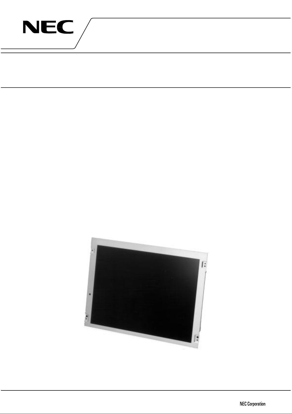
NL10276AC30-04R
TFT COLOR LCD MODULE
38 cm (15.0 inches), 1024
768 pixels, 262,144 colors,
××××
LVDS interface, Wide viewing angle, High luminance
DESCRIPTION
NL10276AC30-04R is a TFT (thin film transistor) active matrix color liquid crystal display (LCD) comprising
amorphous silicon TFT attached to each signal electrode, a driving circuit and a backlight. NL10276AC30-04R has
a built-in backlight with inverter.
The 38 cm (15.0 inches) diagonal display area contains 1024 × 768 pixels and can display 262,144 colors
simultaneously.
FEATURES
• Wide viewing angle (with retardation film)
• High luminance
• Low reflection
• LVDS interface (Equivalent of THC63LVDF64A, THine Electronics, Inc.)
• Incorporated edge type backlight (two lamps, inverter) and Lamp holder replaceable
APPLICATIONS
• Desk-top type of PC
• Engineering work station
• Display terminal for control system
• Monitor for process controller
Document No. EN0490EJ1V0DS00
Date Published April 2000 P
Printed in Japan
The information in this document is subject to change without notice.
Please confirm with the delivery specifi cati on before starting to design the system.
2000©
NL10276AC30-04R
STRUCTURE AND FUNCTIONS
A color TFT (thin film transistor) LCD module is comprised of a TFT liquid crystal panel structure, LSIs for driving
the TFT array, and a backlight assembly. The TFT panel structure is created by sandwiching liquid crystal material
in the narrow gap between a TFT array glass substrate and a color filter glass substrate. After the driver LSIs are
connected to the panel, the backlight assembly is attached to the backside of the panel.
RGB (red, green, blue) data signals from a source system is modulated into a form suitable for active matrix
addressing by the onboard signal processor and sent to the driver LSIs which in turn addresses the individual TFT
cells.
Acting as an electro-optical switch, each TFT cell regulates light transmission from the backlight assembly when
activated by the data source. By regulating the amount of light passing through the array of red, green, and blue
dots, color images are created with clarity.
OUTLINE OF CHARACTERISTICS (at room temperature)
Items Description
Display area 304.128 (H) × 228.096 (V) mm
Drive system a-Si TFT active matrix
Display colors 262,144 colors
Number of pixels 1024 × 768 pixels
Pixel arrangement RGB vertical stripe
Pixel pitch 0.297 (H) × 0.297 (V) mm
Module size 350.0 (H) × 265.0 (V) × 20.0 (typ.) (D) mm
Weight 1350 g (typ.)
Contrast ratio 200 : 1 (typ.)
Viewing angle (more than the
contrast ratio of 10 : 1)
Designed viewing direction • Wider vie w ing an g le without image reversal : up side (12 o’clock)
Color gamut 40% (typ., at center, to NTSC)
Response time 15 ms (typ.), “white 100%” to “black 10%”
Luminance 200 cd/m2 (typ.)
Signal system RGB 6-bit signals, Synchronous signals (Hsync, Vsy nc) , Dot clock (CLK)
Supply voltage 5 V (Logic, LCD driving), 12 V (Backlight)
Backlight Edge light type: Two cold cathode fluorescent lamps with invert er
Power consumption 11.8 W (typ.)
• Horizontal : 60° (typ., left side, right side)
• Vertical : 40° (typ., up side), 50°(typ., down side)
• Wider viewing angle with contrast ratio: down side (6 o ’clock)
γ
• Optimum grayscale (
LVDS interface (Equivalent of THC63LVDF64A, THine Electronics, Inc.) 1 port
• Lamp holder: type No.150 LHS11
• Inverter: type No.141PW201
= 2. 2): perpendicular
2
Data Sheet EN0490EJ1V0DS00
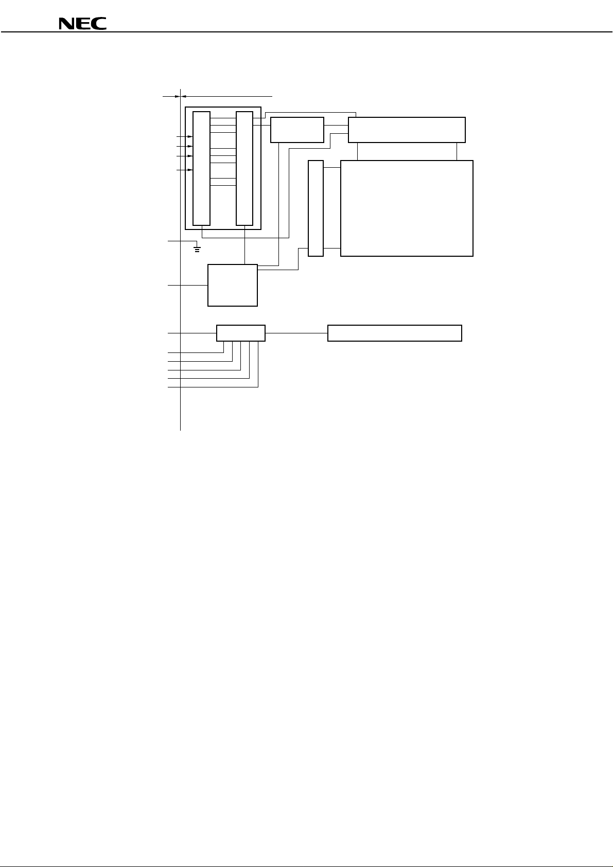
BLOCK DIAGRAM OF BASIC STRUCTURE
NL10276AC30-04R
I/F LCD module
D0 +/–
D1 +/–
D2 +/–
CK +/–
GND
CC
V
V
DDB
ACA
BRTC
BRTH
BRTL
GNDB
IC
Controller
Equivalent of
THC63LVDF64A (THine)
DC/DC
Converter
Inverter
Power supply
for drivers
768
lines
V-driver
H: 1024
V: 768
Backlight (Edge light type)
H-driver
3072 lines
TFT LCD panel
× 3 (R,G,B)
Neither GND nor GNDB is connected to FG (Frame Ground).
Note:
GND and GNDB should be connected to customer equipment FG.
Data Sheet EN0490EJ1V0DS00
3
NL10276AC30-04R
GENERAL SPECIFICATIONS
Items Specifications Unit
Module size 350.0 ± 0.6 (H) × 265.0 ± 0.6 (V) × 20.5 (max.) (D) mm
Display area 304.128 (H) × 228.096 (V) mm
Number of pixels 1024 (H) × 768 (V) pixel
Dot pitch 0.099 (H) × 0.297 (V) mm
Pixel pitch 0.297 (H) × 0.297 (V) mm
Pixel arrangement RGB (Red, Green, Blue) vertical stripe –
Display colors 262,144 (RGB, 6 bit) color
Weight 1350 (typ.), 1500 (max.) g
ABSOLUTE MAXIMUM RATINGS
Parametesrs Symbols Ratings Unit Remarks
Logic input voltage V
Logic input voltage
(backlight-logic signal)
Logic input voltage
(backlight-BRTL signal)
Storage temp. T
Operating temp. T
Relative humidity (RH)
Absolute humidity
Note 1:
Note 2:
Measured at the LCD panel of the module.
No Condensation.
CC
V
DDB
V
I
IBL1
V
IBL2
V
ST
OP
Note 2
Note 2
–0.3 to +6.0 VSupply voltage
–0.3 to +14 V
–0.3 to VCC + 0.3 V
–0.3 to +5.5 V
–0.3 to +1.5 V
–20 to +60 °C
0 to +50 °C
≤
95 % T
≤
85 % 40 < T
Absolute humidity shall not exceed
a
= 50°C, Relative humidity =
T
85% level.
g/m
a
T
= 25°C
Module surface
a
≤ 40°C
3
Ta > 50°C
a
≤ 50°C
Note 1
4
Data Sheet EN0490EJ1V0DS00
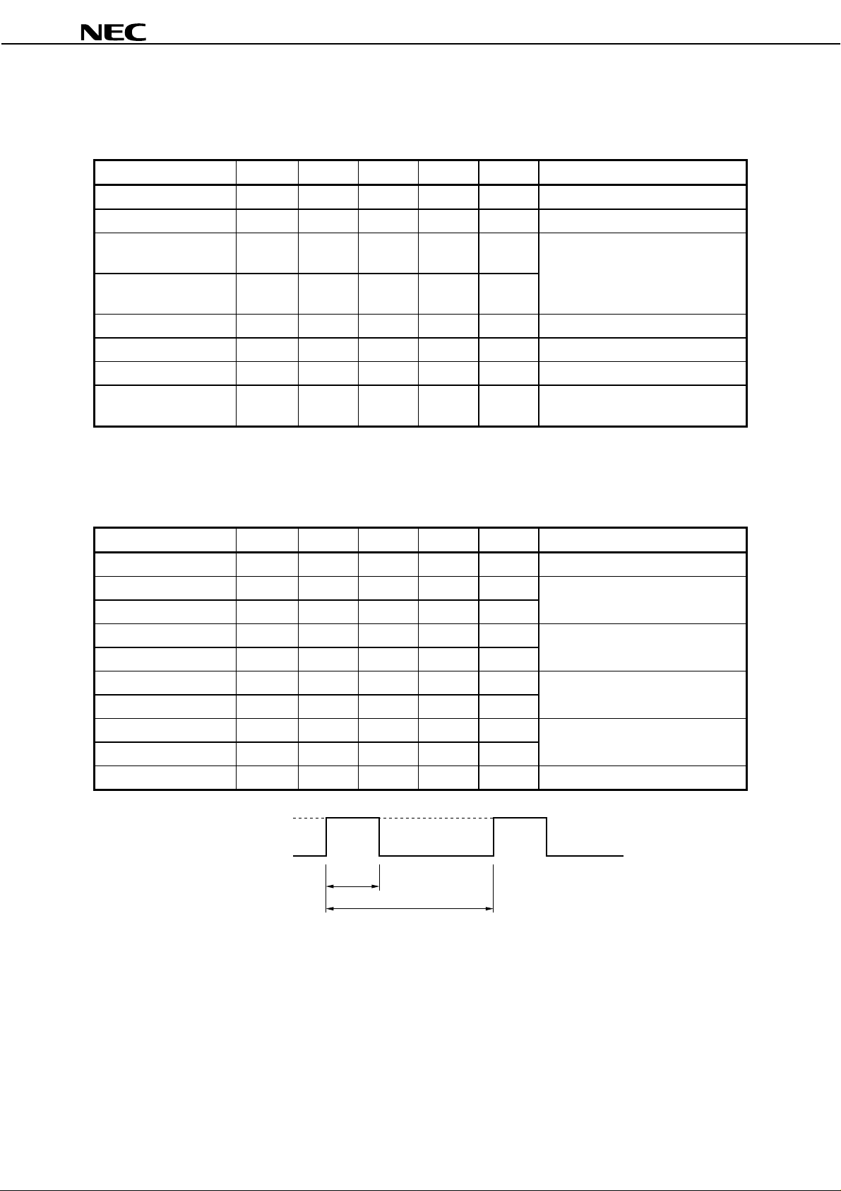
ELECTRICAL CHARACTERISTICS
(1) Logic, LCD driving
Parameter Symbol Min. Typ. Max. Unit Remarks
NL10276AC30-04R
a
= 25°C
T
Supply voltage V
Ripple voltage V
LVDS signal input “L”
voltage
LVDS signal input “H”
CC
RP
IL
V
IH
V
4.75 5.0 5.25 V –
– – 100 mV for V
–100 – – mV
CM
= 1.2 V
V
CM
: Common mode voltage in LVDS
V
– – +100 mV
voltage
Input voltage V
Common mode voltage V
Terminating resistor R
Supply current I
I
CM
T
CC
0.25 0.35 0.45 V –
1.125 1.25 1.375 V RT = 100
– 100 –
– 300
600 mA VCC = 5.0 V
Ω
Note
Checkered flag pattern (in EIAJ ED-2522)
Note:
(2) Backlight
Parameters Symbols Min. Typ. Max. Unit Remarks
Supply voltage V
Logic input “L” voltage 1 V
Logic input “H” voltage 1 V
Logic input “L” voltage 2 V
Logic input “H” voltage 2 V
Logic input “L” current 1 I
Logic input “H” current 1 I
Logic input “L” current 2 I
Logic input “H” current 2 I
Supply current I
DDB
IL1
IH1
IL2
IH2
DDB
10.8 12.0 13.2 V –
IL1
IH1
IL2
IH2
0–0.6V
4.5 – 5.25 V
0–0.8V
2.2 – 5.25 V
–1.0 – – mA
for BRTP
for BRTC, ACA, BRTL
for BRTP
––10mA
–1.0 – – mA
for BRTC, ACA, BRTL
––0.8mA
– 860 1000 mA V
DDB
= 12.0 V (at max. luminance)
CC
driver
Ω
–
a
= 25°C
T
860 (mA) typ.
0 (mA)
Duty
Luminance control frequency
maximum luminance control: 100 % (Duty)
minimum luminance control: 20 % (Duty)
Luminance control frequency: 243 to 297 Hz 270 Hz (typ.)
Data Sheet EN0490EJ1V0DS00
5
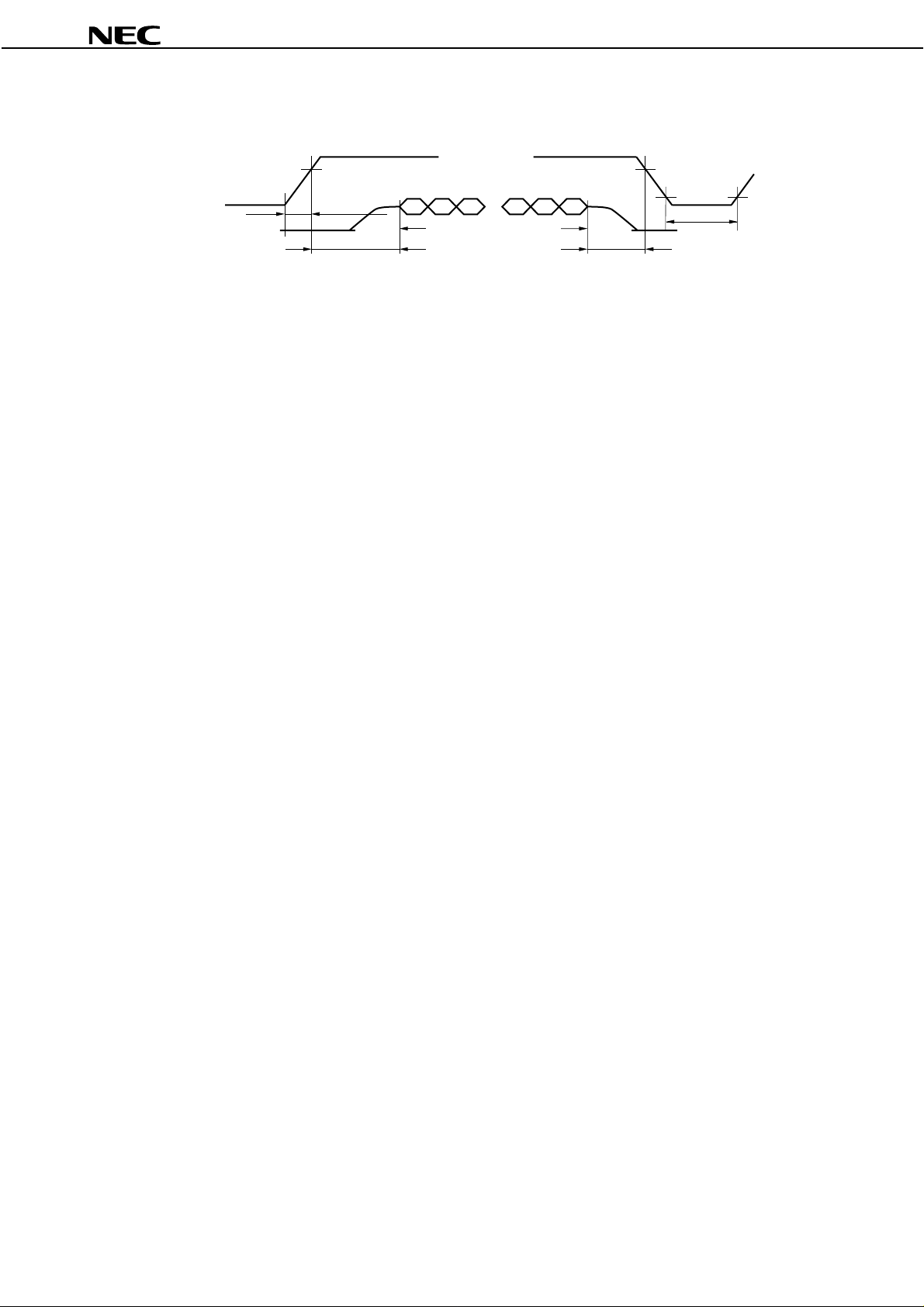
SUPPLY VOLTAGE SEQUENCE
CC
ON VCC OFF
V
V
CC
0 V
Signals
4.75 V
Tr < 80 ms
0 V
NL10276AC30-04R
0.5 V
t > 200 ms
Valid
Notes 1:
10 < t < 35 ms
Logic signals (synchronous signals and control signals) must be “0” voltage(V), when V
0 < t < 35 ms
CC
is not input.
If input voltage to signal lines is higher than 0.3 V, the internal circuit will be damaged.
The supply voltage for input signals should be the same as VCC.
2:
DDB
3:
Apply V
within the LCD operation period. (more than 4 Vsync after the Vcc are input.) When the
backlight turns on before LCD operation or the LCD operation turns off before the backlight turns off,
the display may momentarily become white.
However, 12 V for backlight should be started up within 80 ms, otherwise, the protection circuit makes
the backlight turns off.
When the power is off, please keep whole signals low level or high impedance.
4:
6
Data Sheet EN0490EJ1V0DS00
NL10276AC30-04R
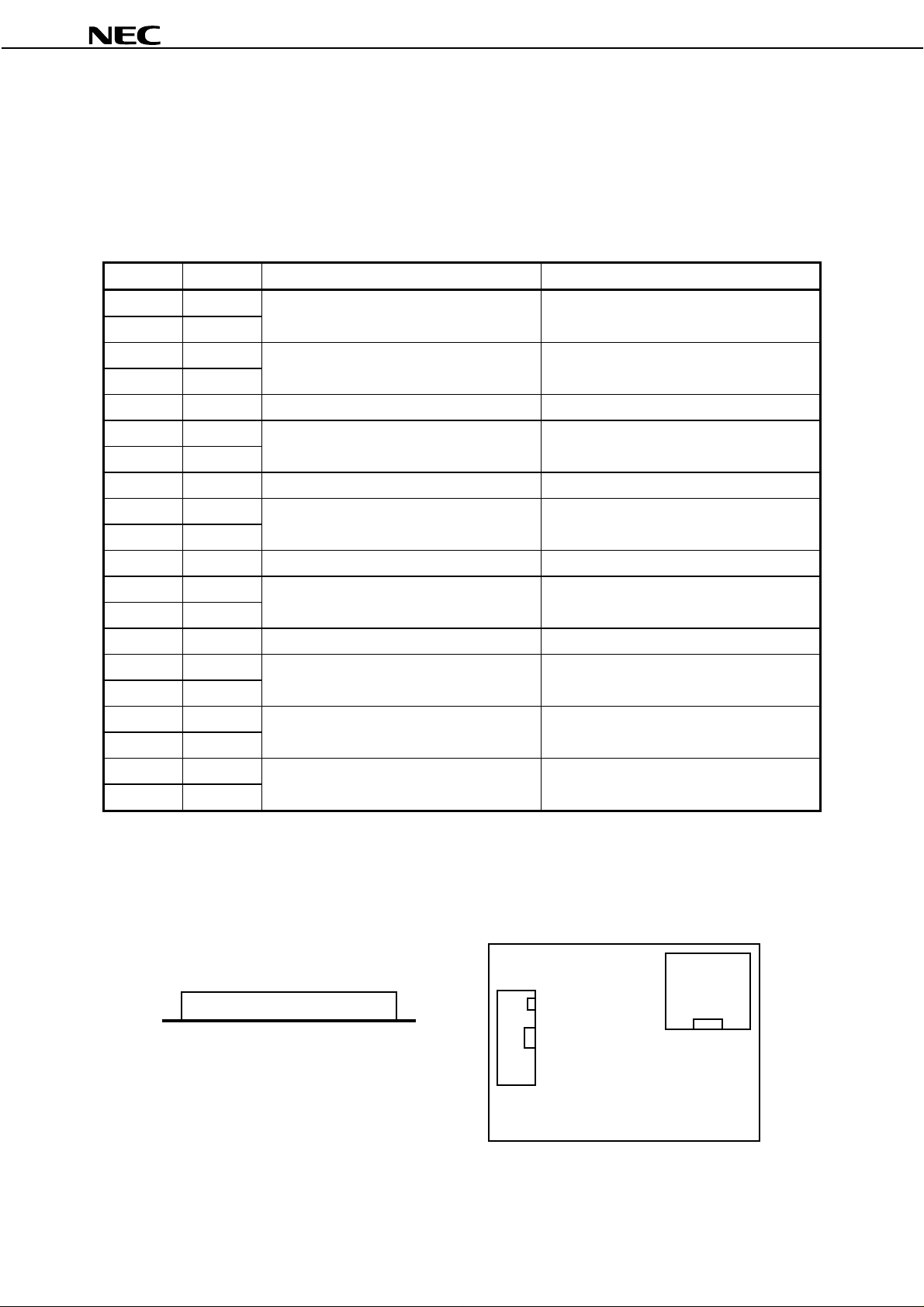
INTERFACE AND CONNECTOR PIN ASSIGNMENT
(1) Interface connector for signal and power
Part No. : FI-SE20P-HF
Adaptable socket: FI-SE20M
Supplier : Japan Aviation Electronics Industry Limited (JAE)
CN1
Pin No. Symbol Signal type Function
1GND
2GND
3NC
4NC
5 GND Ground
6CK+
7CK–
8 GND Ground
9D2+
10 D2–
11 GND Ground
12 D1+
13 D1–
14 GND Ground
15 D0+–
16 D0–
17 GND
18 GND
19 V
20 V
CC
CC
Ground
Non-connection –
Pixel clock CLK for pixel data f = 65 MHz (typ.)
Pixel data LVDS differenti al data input
Pixel data LVDS differenti al data input
Pixel data LVDS differenti al data input
Ground
+5.0 V power supply Supply +5.0 V ±5%
Note 1
Note 1
(LVDS level)
Note 1
Note 1
Note 1
Note 1
Notes 1:
2:
20 19 · · · · · 2 1
GND is Signal ground for logic and LCD driving. The GND should be connected to system
ground. The GND is not connected to FG (Frame Ground) in this module.
Connect all pins (expect 3.4) to the appointed places to avoid noise problems.
Use 100 Ω twist pair wires for the cable.
CN1: Figure from socket view
1
CN202
9
CN201
1
←Insert direction
11
CN1
20 1
↑
Insert direction
Note: CN202 should be opened.
Data Sheet EN0490EJ1V0DS00
7
NL10276AC30-04R
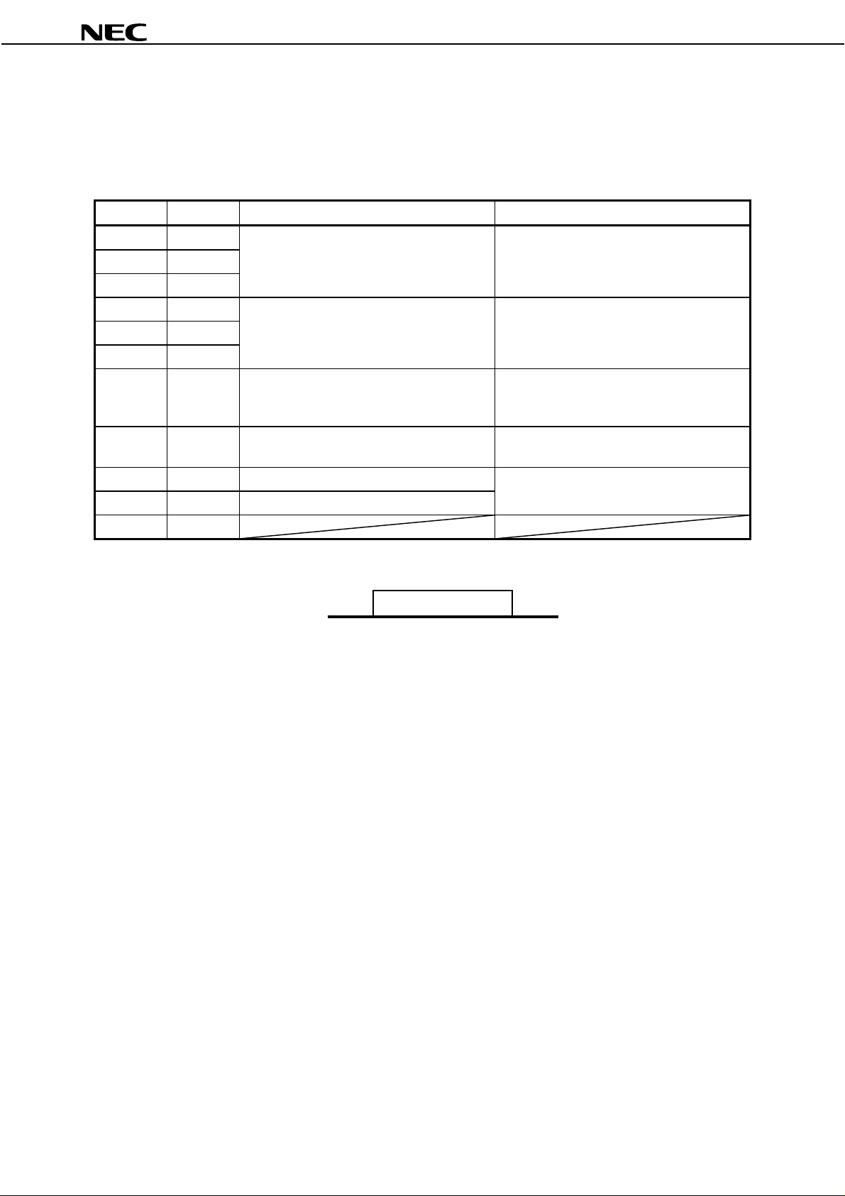
(2) Connector for backlight unit
Part No. : IL-Z-11PL1-SMTY
Adaptable socket: IL-Z-11S-S125C3
Supplier : Japan Aviation Electronics Industry Limited (JAE)
CN201
Pin No. Symbol Signal type Function
1V
2V
3V
4 GNDB
5 GNDB
6 GNDB
7 ACA Luminance control signal “H” or “Open”: Normal luminance (100%)
8 BRTC Backlight ON/OFF control signal “H” or “Open”: Backlight ON
9 BRTH Luminance control signal
10 BRTL Luminance control signal
11 N.C.
DDB
DDB
DDB
12 V power supply Supply +12 V ±10 %
Ground for backlight
CN201: Figure from socket view
· · · · · 2 1
311 10
Note 1
“L” : Low luminance (1/2 of the
normal luminance)
“L” : Backlight OFF
Note 2
8
Data Sheet EN0490EJ1V0DS00
NL10276AC30-04R
Part No. : IL-Z-9PL1-SMTY
Adaptable socket: IL-Z-9S-S125C3
Supplier : Japan Aviation Electronics Industry Limited (JAE)
CN202
Pin No. Symbol Signal type Function
1 GNDB
2 GNDB
3 ACA Luminance control signal “H” or “Open”: Normal luminance (100%)
4 BRTC Backlight ON/OFF control signal “H” or “Open”: Backlight ON
5 BRTH Luminance control signal-1
6 BRTL Luminance control signal-1
7 BRTP Luminance control signal-2
8 GNDB Ground for backl i ght
9 PWSEL Luminance control select signal “H” or “Open”: Variable resistor control or
Notes 1:
Neither GND nor GNDB connected to FG (Frame Ground) in this module. They should be connected to
Ground for backlight
Note 1
“L” : Low luminance (1/2 of the
normal luminance)
“L” : Backlight OFF
Note 2
Note 3
Note 1
voltage control (Note 2)
“L” : BRTP signal control (Note 3)
the FG of customer equipment.
The ways to controll luminance are as follows.
2:
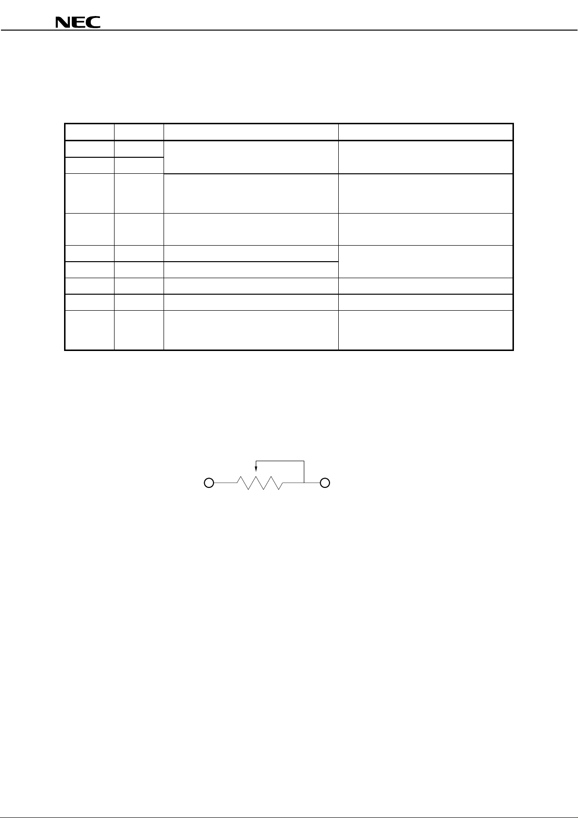
(1) A way of luminance control by a variable resistor.
The variable resistor for luminance control should be 10 kΩ , and zero point of the resistor
corresponds to the minimum of luminance.
BRTH BRTL
R
Mating variable resistor
Maximum luminance (100 %)
Minimum luminance (30 %)
: 10 kΩ ±5% (1/10 W), B curve
: R = 10 KΩ
: R = 0 Ω
(2) A way of luminance control by voltage
BRTH should be fixed to 0 V to control luminance by voltage. The range of input voltage between
BRTL and GNDB is as follows.
Maximum luminance (100%, ACA = H) : 1 V (typ.)
Minimum luminance (30%, ACA = H): 0 V
Data Sheet EN0490EJ1V0DS00
9
 Loading...