

NEC NL10276AC30-03 Datasheet

DATA SHEET
NL10276AC30-03
TFT COLOR LCD MODULE
38 cm (15.0 inches), 1024
××××
768 pixels,
FULL-COLOR, MULTI-SCAN FUNCTION
Wide viewing angle
DESCRIPTION
NL10276AC30-03 is a TFT(thin film transistor) active matrix color liquid crystal display (LCD) comprising
amorphous silicon TFT attached to each signal electrode, a driving circuit and a backlight. NL10276AC30-03 has a
built-in backlight with an inverter.
The 38cm (15.0 inches) diagonal display area contains 1024 × 768 pixels and can display full-color (more than
16 million colors simultaneously). Also, it has multi-scan function.
FEATURES
• High luminance
• Low reflection
• Wide viewing angle (with Retardation Film)
• Analog RGB signals
• Multi-scan function: e.g., XGA, SVGA, VGA, VGA-TEXT, PC-9801, MAC
• Incorporated edge type backlight (Two lamps, Inverter)
• Lamp holder replaceable (Part No. 150LHS03)
APPLICATIONS
• Desk-top type of PC
• Engineering work station
Regarding the use of OSD, please note that there is possibility of conflicts with a patent in Europe and the U.S.
Thus, if such conflict might happen when you use OSD, we shall not be responsible for any trouble.
Document No. EN0416EJ1V0DS00 (1st edition)
Date Published January 1999 P
Printed in Japan
1999©

NL10276AC30-03
STRUCTURE AND FUNCTIONS
A color TFT (thin film transistor) LCD module is comprised of a TFT liquid crystal panel structure, LSIs for driving
the TFT array, and a backlight assembly. The TFT panel structure is created by sandwiching liquid crystal material
in the narrow gap between a TFT array glass substrate and a color filter glass substrate. After the driver LSIs are
connected to the panel, the backlight assembly is attached to the backside of the panel.
RGB (red, green, blue) data signals from a source system is modulated into a form suitable for active matrix
addressing by the onboard signal processor and sent to the driver LSIs which in turn addresses the individual TFT
cells.
Acting as an electro-optical switch, each TFT cell regulates light transmission from the backlight assembly when
activated by the data source. By regulating the amount of light passing through the array of red, green, and blue
dots, color images are created with clarity.
OUTLINE OF CHARACTERISTICS (at room temperature)
Display area 304.128 (H) × 228.096 (V) mm
Drive system a-Si TFT active matrix.
Display colors Full-color
Number of pixels 1024 × 768
Pixel arrangement RGB vertical stripe
Pixel pitch 0.297 (H) × 0.297 (V) mm
Module size 350.0 (H) × 265.0 (V) × 20.0 (D) mm
Weight 1400 g (typ.)
Contrast ratio 200:1 (typ., perpendicular)
Viewing angle (more than the contrast ratio of 10:1)
• Horizontal: 55° (typ., left side, right side)
• Vertical : 50° (typ., up side), 45° (typ, down side)
Designed viewing direction
• Wider viewing angle with contrast ratio : Down side (6 o’clock)
• Wider viewing angle without image reversal: up side (12 o’clock)
= 2.2) : perpendicular
• Optimum grayscale (
Color gamut 42 % (typ., At center, To NTSC)
Response time 15 ms (typ.), “white” to “black”
Luminance 200 cd/m
Signal system Analog RGB signals, Synchronous signals (Hsync and Vsync), CLK
Supply voltage 12 V, 12 V (Logic/LCD driving, Backlight)
Backlight Edge light type: Two cold cathode fluorescent lamps with an inverter
Power consumption 15.6 W (typ.)
2
(typ.)
γ
[Replaceable parts]
• Lamp holder : 150LHS03
• Inverter : 150PW031
2
Data Sheet EN0416EJ1V0DS00
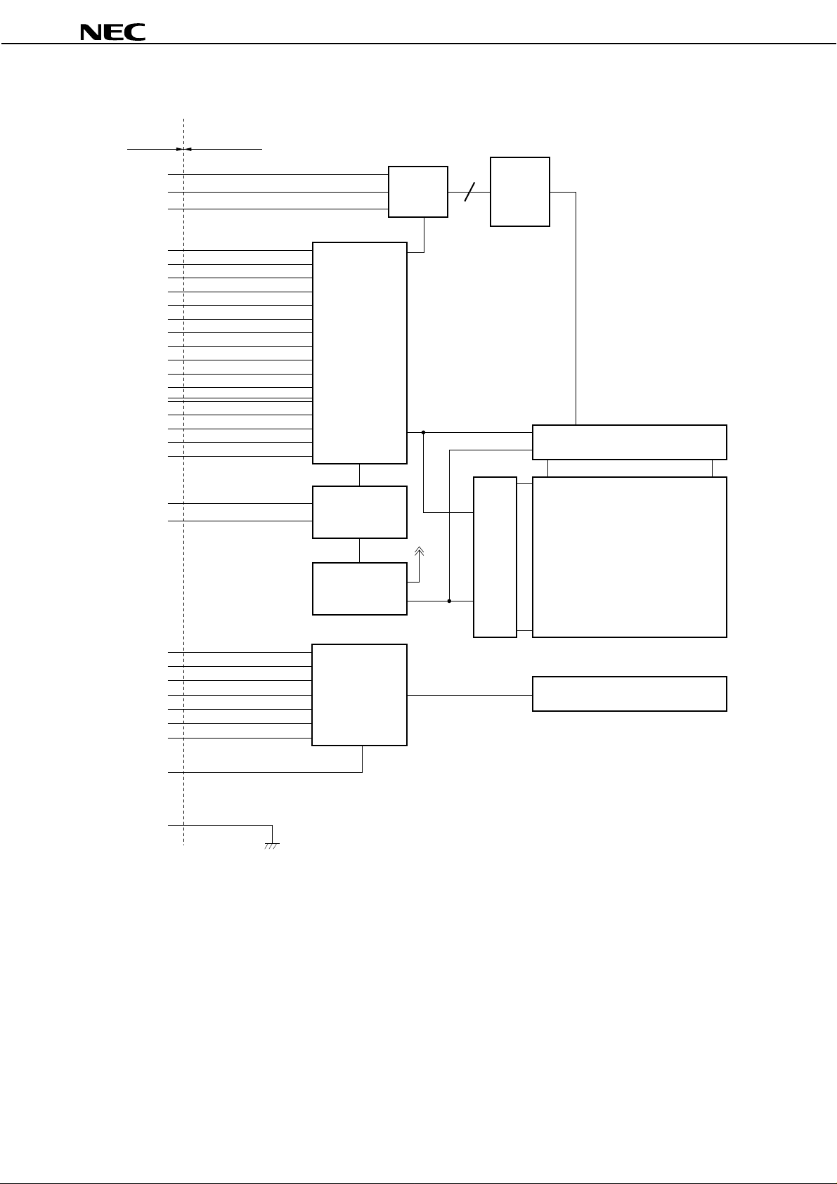
BLOCK DIAGRAM
NL10276AC30-03
I/F
R
G
B
Hsync
Vsync
CLK
DESEL
CLAMP
CPSEL
CNTDAT
CNTCLK
CNTSTB
CNTSEL
OSDENI
OSDRI
OSDGI
OSDBI
ADJSEL
CNTSTB2
POWC
VDD
LCD module
Timing controller
ON/OFF
AIF
V-driver
AMP
H-driver
3072 lines
LCD panel
768 lines
V
DD
B
BRTC
BRTH
BRTL
ACA
BRTP
PWSEL
GNDB
GND
Frame is not connected to GND and GNDB.
Note
DC/DC
converter
Inverter
HV: 1024 × 3 (R, G, B)
: 768
Backlight
Data Sheet EN0416EJ1V0DS00
3

NL10276AC30-03
SPECIFICATIONS
GENERAL SPECIFICATIONS
Item Contents Unit
Module size 350.0 ± 0.6 (H) × 265.0 ± 0.6 (V) × 20.5 (max.) (D) mm
Display area 304.128 (H) × 228.096 (V) mm
Number of dots 1024 × 3 (H) × 768 (V) dots
Pixel pitch 0.297 (H) × 0.297 (V) mm
Dot pitch 0.099 (H) × 0.297 (V) mm
Pixel arrangement RGB (Red, Green, Blue) vertical stripe –
Display colors Full color color
Weight 1500 (max.) g
ABSOLUTE MAXIMUM RATINGS
Parameter Symbol Rating Unit Remarks
DD
V
DD
B –0.3 to +14 V
V
Logic input voltage Vin1 –0.3 to +5.5 V
R, G, B input voltage Vin 2 –6.0 to +6.0 V
CLK input voltage Vin 3 –7.0 to +7.0 V
BRTL input voltage Vin 4 –0.3 to +1.5 V
Storage temp. Tst –20 to + 60 °C –
Operating temp. Top 0 to +50 °C
Humidity
(no condensation)
Absolute humidity shall not exceed Ta = 50°C,
Measured at the display area
Note
–0.3 to +14 VSupply voltage
≤
95% relative humidity Ta ≤ 40°C
≤
85% relative humidity 40 < Ta ≤ 50°C
85% relative humidity level.
Ta = 25°C
Ta = 25°C
DD
= 12 V
V
Module surface
Ta > 50°C
Note
4
Data Sheet EN0416EJ1V0DS00

ELECTRICAL CHARACTERISTICS
(1) Logic, LCD driving, Backlight
Item Symbol Min. Typ. Max. Unit Remarks
DD
V
DD
B 11.4 12.0 12.6 V f or backlight
V
Logic input “L” voltage 1 V
Logic input “H” voltage 1 V
Logic input “L” voltage 2 V
Logic input “H” voltage 2 V
Input CLK voltage V
Input DC voltage level V
Logic input “L” current 1 I
Logic input “H” current 1 I
Logic input “L” current 2 I
Logic input “H” current 2 I
Logic input “L” current 3 I
Logic input “H” current 3 I
Logic input “L” current 4 I
Logic input “H” current 4 I
Logic input “L” current 5 I
Logic input “H” current 5 I
Supply current
IL1
IH1
IL2
IH2
ICLK
IDCCLK
IL1
IH1
IL2
IH2
IL3
IH3
IL4
IH4
IL5
IH5
DD
I
DD
B – 750 850 mA VDDB = 12.0 V
I
11.4 12.0 12.6 V for Logic and LCD drivingSupply voltage
0–0.6V
4.5 – 5.25 V
0–0.8V
2.2 – 5.25 V
0.6–1.0Vp-p
–4.5 – +4.5 V
–10 – –
– – 160
–1400 – –
––10
µ
A
µ
A
µ
A
µ
A
–1.0 – – mA
––0.8mA
–1.0 – – mA
––10mA
–10 – –
––10
µ
A
µ
A
– 550 800 mA
NL10276AC30-03
(Ta = 25°C)
for BRTP
Logic except BRTP
CLK
Hsync, Vsync
CNTSEL, CPSEL , POW C, ADJSEL
BRTC, BRTL, ACA, PWSEL
BRTP
Logic except inputs above
DD
V
= 12.0 V
(Max. luminance)
Note
Pixel checkered pattern
Note
(2) Video signal (R, G, B) input
Item Min. Typ. Max. Unit Remarks
Maximum amplitude (white - black) 0
DC input level (black)
(3) CLK input equivalent circuit
CLK
0.7
(black)
−
3.5 – +3.5 V –
(white)
0.9 Vp-p Contrast adjustment is needed if the
amplitude exceeds 0.7 Vp-p.
1000 pF
510 Ω
(Ta = 25°C)
Data Sheet EN0416EJ1V0DS00
5

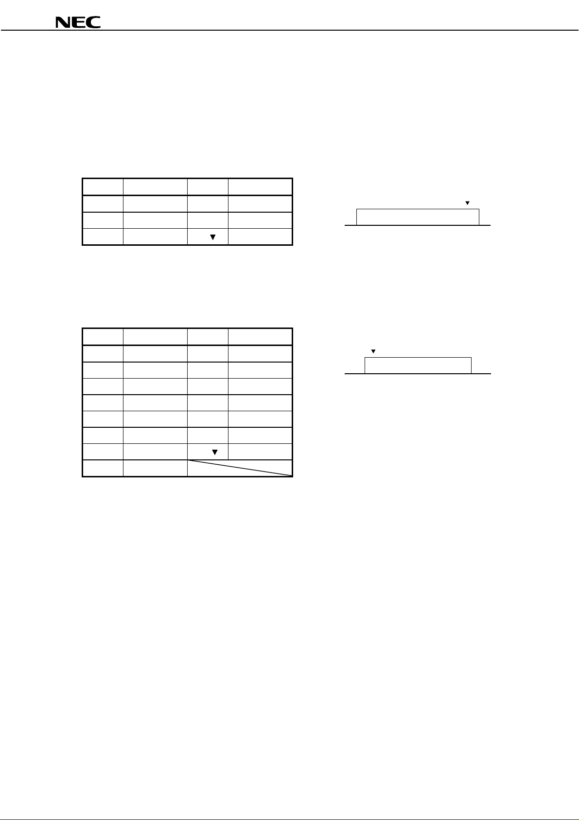
SUPPLY VOLTAGE SEQUENCE
(1) Sequence of power supply
Voltage
200 ms ≤
Synchronous signals, Control signals, CLK.
Note
CAUTION
Wrong power sequence may cause damage to the module.
Logic signals Note
POWC
V
30 ms ≤
NL10276AC30-03
DD
Time
0 ms <
0 ms <
a) Logic signals (synchronous signals and control signals) should be “0” voltage (V), when VDD is not input.
If higher than 0.3 V is input to signal lines, the internal circuit will be damaged.
b) LCD module will shut down the power supply of driving voltage to LCD panel internally when one of
CLK, Hsync, Vsync is not input more than 90 ms typically. As the display data are unstable in this
period, the display is disordered. But the backlight works correctly even in this period. So the backlight
ON/OFF should be controlled by BRTC signal.
c) The backlight ON/OFF (BRTC signal) should be controlled while logic signals are supplied. The
DD
backlight power supply (V
B) is not related to the power supply sequence. However, unstable data is
displayed when the backlight power is turned ON without logic signals.
DD
d) Keep POWC signal “L” more than 200 ms after the power supply (V
B) is input , if POWC signal is
controlled.
e) Analog RGB input are independent of this power supply sequence.
f) 12 V for backlight should be started up within 80 ms, otherwise the protection circuit makes the backlight
turn off.
6
Data Sheet EN0416EJ1V0DS00

NL10276AC30-03
(2) Ripple of supply voltage
Please note that the ripple at the input connector of the module should be within the values shown in this table.
If the ripple is beyond these values, the noise may appear on the screen.
Acceptable range
The acceptable range of ripple voltage includes spike noise.
Note
DD
V
(for logic and LCD driver)
≤
100 mVp-p
DD
V
B
(for backlight)
≤
200 mVp-p
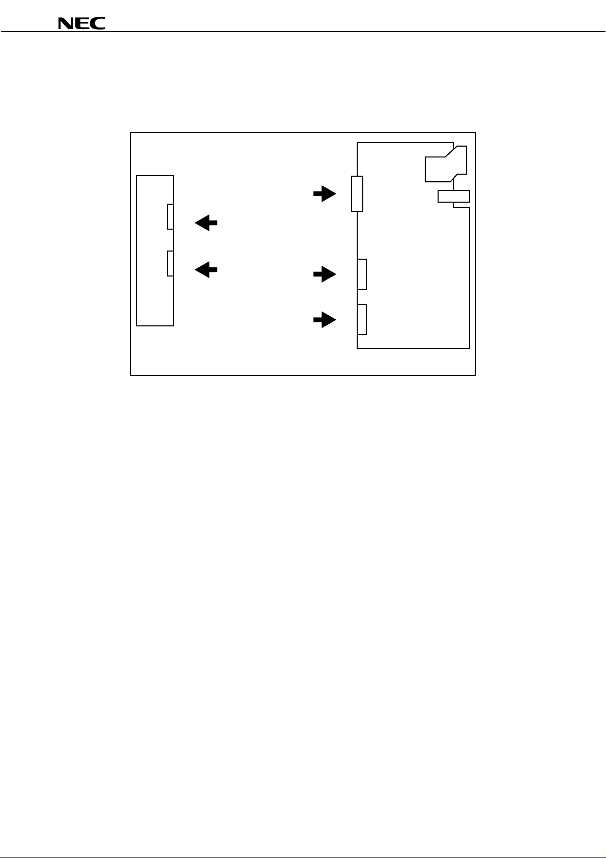
Examples of the power supply connection
a) Separate the power supply b) Put the filter
Power VDD
Power VDDB
Power
Filter VDD
Filter VDDB
(3) Inverter current wave
In the luminance control mode, the rush current below flows into the inverter of the module. The duty cycle
varies from 100% through 20% depending on the luminance control level. This might cause the noise on the
screen. Please evaluate the appropriate value of the capacitor in the filter to eliminate the noise.
Filter
Inverter circuit of NL10276AC30-03
Customer’s Power
supply
(12 V)
Rush current
GND
0 (A)
to V
DD
750 (mA)
Duty
Frequency*
* Frequency:
Vsync frequency × K*
* Vsync ≤ 75 Hz: K = 4.6
> 75 Hz: K = 3.6
Data Sheet EN0416EJ1V0DS00
7
INTERFACE PIN CONNECTION
(1) CN1
Part No. : MRF03-6R-SMT
Adaptable socket: MRF03-6PR-SMT (board-to-board type)
MRF-03-6P-0.8D (cable type)
MRF-03-6P-1.27 (cable type)
Supplier : HIROSE ELECTRIC CO., LTD.
NL10276AC30-03
Pin No. Symbol Pin No. Symbol
1B4Vsync
2 G 5 Hsync
3R6CLK
(2) CN3
Part No. : IL-Z-15PL-SMTY
Adaptable socket: IL-Z-15S-S125C3
Supplier : Japan Aviation Electronics Industry Limited (JAE)
Pin No. Symbol Pin No. Symbol
1VDD9GND
2VDD10 CNTCLK
3 GND 11 CPSEL
4 GND 12 CLAMP
5POWC13GND
6 CNTSE L 14 N.C.
7 CNTDAT 15 GND
8 CNTSTB
Figure from socket view
······12 56
Figure from socket view
····15 14 12
N.C. (No connection) should be open.
Note
8
Data Sheet EN0416EJ1V0DS00

(3) CN3
Part No. : DF14A-20P-1.25H
Adaptable socket: DF14-20S-1.25C
Supplier : HIROSE ELECTRIC CO., LTD
NL10276AC30-03
Pin No. Symbol Pin No. Symbol
1 GND 11 ADJSEL
2 OSDENI 12 N.C.
3 GND 13 CNTSTB2
4OSDBI14GND
5 GND 15 N.C.
6 OSDGI 16 GND
7 GND 17 N.C.
8 OSDRI 18 N.C.
9 GND 19 N.C.
10 N.C. 20 N.C.
N.C. (No connection) should be open.
Note
(4) CN201
Part No. : IL-Z-11PLI-SMTY
Adaptable socket: IL-Z-11S-S125C3
Supplier : Japan Aviation Electronics Industry Limited (JAE)
Figure from socket view
····12 2019
Pin No. Symbol Pin No. Symbol
1V
2V
3V
4 GNDB 10 BRTL
5 GNDB 11 N.C.
6 GNDB
DD
B7ACA
DD
B8BRTC
DD
B9BRTH
(5) CN202
Part No. : IL-Z-9PL1-SMTY
Adaptable socket: IL-Z-9S-S125C3
Supplier : Japan Aviation Electronics Industry Limited (JAE)
Pin No. Symbol Pin No. Symbol
1 GNDB 6 B RT L
2 GNDB 7 BRTP
3 A CA 8 GNDB
4BRTC9PWSEL
5BRTH
Figure from socket view
11 10
···· 12
Figure from socket view
···· 12
98
N.C. (No connection) should be open.
Note
Data Sheet EN0416EJ1V0DS00
9
Caution For CN201 and CN202, pins with an identical symbol are connected inside the module.
<Rear view>
NL10276AC30-03
Do not use both of these pins at the same time.
1
11
CN202
1
9
CN201
1
CN1
6
15
CN3
1
1
CN4
20
10
Data Sheet EN0416EJ1V0DS00

NL10276AC30-03
PIN FUNCTION
Symbol I/O Logic Description
CLK Input Positive Dot clock input . (ECL level ) This timing-signal is for display data.
Hsync I nput Negativ e Horizontal synchronous signal input (TTL level)
Vsync Input Negative Vertical synchronous signal input (TTL level)
R Input – Red video signal input (0.7 Vp-p, 75 Ω)
G Input – Green video signal input (0.7 Vp-p, 75 Ω)
B Input – Blue video signal input (0.7 Vp-p, 75 Ω)
POWC Input Positive Power control signal (TTL level)
“H” or “Open”: Logic and LCD power are on.
“L” : Logic and LCD power are off.
When POWC is “L”, serial communication data is cleared.
Please set again.
CNTSEL Input – Display control signal in case of serial communications. (TTL level)
“H” or “Open” : Default , “L” : External control
External control is set up by serial communication.
CNTDAT Input Positive Dis pl ay cont rol data (TTL level)
Detail of CNTDAT is mentioned in
CNTCLK Input Positive
CNTSTB Input Positive Lat ch pulse for display control data (TTL level)
CPSEL Input – CLAMP function select signal
CLAMP Input Negative Clamp timing signal of black level (TTL level)
ADJSEL Input Positive Contrast, brightness select control signal (TTL level)
CNTSTB2 Input P ositive Latch pulse2 for display control data
OSDRI Input – Input OSD-R data
OSDGI Input – Input OSD-G data
OSDBI Input – Input OSD-B data
OSDENI Input Positive Enable signal for OSD
CLK for display control data (TTL level)
Detail of CNTCLK is mentioned in
Detail of CNTSTB is mentioned in
“H” or “Open”: Default , “L” : External control
This mode works when CPSEL = “L”.
“H” or “Open”: Default , “L” : External control
Detail of CNTSTB2 is mentioned in
Detail is mentioned in
Detail is mentioned in
Detail is mentioned in
Detail is mentioned in
OSD FUNCTIONS
OSD FUNCTIONS
OSD FUNCTIONS
OSD FUNCTIONS
FUNCTIONS.
FUNCTIONS.
FUNCTIONS.
FUNCTIONS
(1/2)
Data Sheet EN0416EJ1V0DS00
11
NL10276AC30-03
Symbol I/O Logic Description
ACA Input Positive Luminance control signal (TTL level)
“H” or “Open”: Normal luminance
“L” : Low luminance (1/2 of normal luminance)
BRTC Input Positive Backlight ON/OFF control signal (TTL level)
“H” or “Open”: Backlight ON, “L” : Backlight OFF
BRTH
BRTL
BRTP Input – Luminance control signal
PWSEL Input Positive
DD
V
VDDB – – Power supply for backlight. +12 V (±5 %)
GND – – Signal ground for Logic and LCD driving (Connect to system ground)
GNDB – – Ground for backlight, GNDB is not connected to the frame ground of LCD
Input – Variable resistor control of Voltage control
See [Function select] for detail.
Select the control of luminance (TTL level)
See [Function select] for detail.
– – Power supply for Logic and LCD driving +12 V (±5 %)
module.
(2/2)
Frame ground, system ground (GND) and backlight ground (GNDB) are not connected in the module.
Note
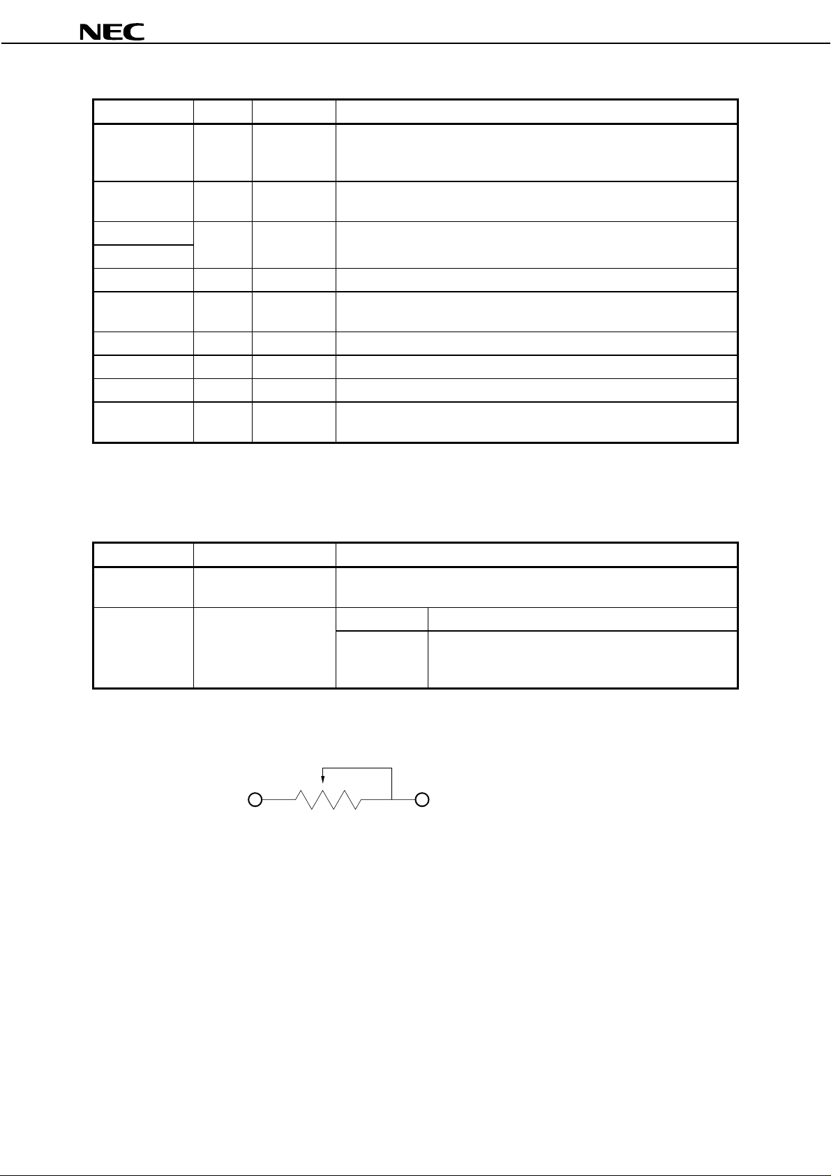
[Function select]
BRTP PWSEL How to adjust
Valid “L” Luminance can be controlled by BRTP signal.
See
OUTSIDE CONTROL FOR LUMINANCE
Open “H” or “Open”
The variable resistor for luminance control should be 10 kΩ type, and zero point of the resistor correspond
Note
Volume
Voltage
Please connect BRTP and BRTL.
Fix BRTH to “0 V” and input proper voltage to BRTL.
1 V: maximum luminance (100%)
0 V: minimum luminance (20%)
to the minimum of luminance.
Mating variable resistor:
BRTH BRTL
R
Maximum luminance (100 %)
Minimum luminance (20 %)
: R = 10 KΩ
: R = 0 Ω
10 KΩ ± 5 %, B curve
for more detail.
Note
12
Data Sheet EN0416EJ1V0DS00
 Loading...