

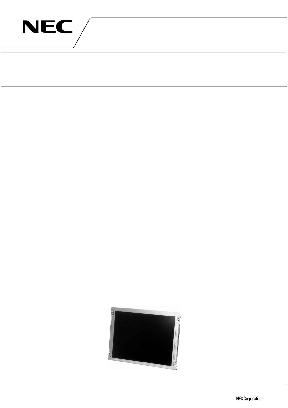
NEC NL10276AC30-01A Datasheet
DATA SHEET
NL10276AC30-01A
TFT COLOR LCD MODULE
38 cm (15 inches), 1024
××××
768 pixels, Full-color,
Multi-scan Function, Built-in backlight with inverter
Ultra wide viewing angle
DESCRIPTION
NL10276AC30-01A is a TFT (thin film transistor) active matrix color liquid crystal display (LCD) comprising
amorphous silicon TFT attached to each signal electrode, a driving circuit, a CRT interface board and a backlight.
NL10276AC30-01A has a built-in backlight with an inverter.
The 38cm (15” inches) diagonal display area contains 1024 × 768 pixels and can display full-color (more than 16
million colors simultaneously). Also, it has ultra-wide viewing angle and multi-scan function. Therefore, this module
calls Super Fine TFT.
CRT interface board installed in this module allows you to achieve the LCD monitor with an analog RGB
interface.
FEATURES
Ultra wide viewing angle
•
Multi-scan function
•
• e.g. XGA, SVGA, VGA, VGA-TEXT, PC9801, MAC
High luminance
•
Incorporated edge type backlight (Four
•
lamps into two lamp holders, Inverter)
Lamp holder replaceable (Part No. 150LHS01)
•
On Screen Display
•
CRT interface board
•
• Auto recognition of input signal
Analog RGB signals, Sync on green, Synchronous
signals (HS, Vsync, Composite)
• Digital control: e.g. Brightness, Display position, Contrast,
CLK delay
• Free supply voltage sequence
• Corresponding to DDC1 and DDC2B
• Corresponding to VESA DPMS
Regarding the use of OSD, please note that there is possibility of conflicts with a patent in Europe and the U.S.
Thus, if such conflict might happen when you use OSD, we shall not be resposible for any trouble.
VESA : Video Electronics Standards Association
DPMS : Display Power Management Signaling
DDC1 : Display Data Channel 1
DDC2B : Display Data Channel 2B
APPLICATIONS
• Engineering workstation (EWS), Desk-top type of PC
The information in this document is subject to change without notice.
Document No. EN0417EJ1V0DS00 (1st edition)
Date Published January 1999 P
Printed in Japan
1999©
NL10276AC30-01A
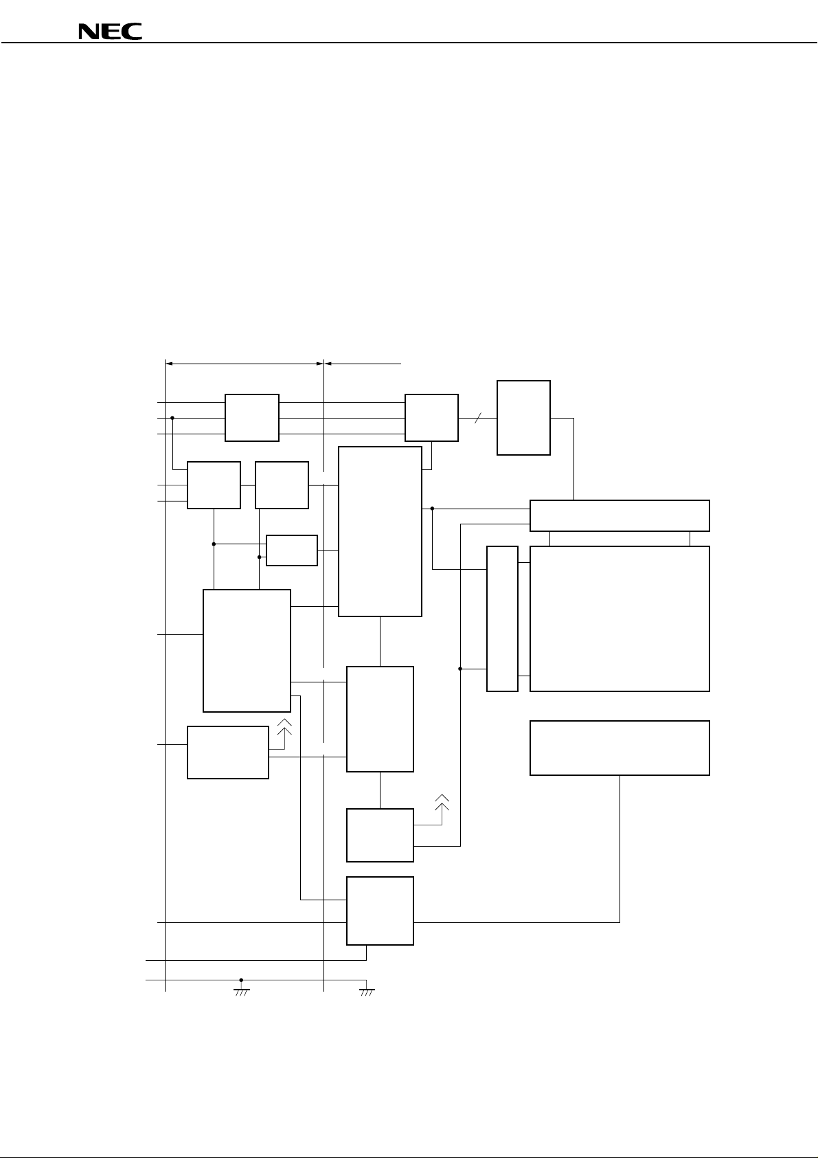
STRUCTURE AND FUNCTIONS
A color TFT (thin film transistor) LCD module is comprised of a TFT liquid crystal panel structure, LSIs for driving
the TFT array, and a backlight assembly. The TFT panel structure is created by sandwiching liquid crystal material
in the narrow gap between a TFT array glass substrate and a color filter glass substrate. After the driver LSIs are
connected to the panel, the backlight assembly is attached to the backside of the panel.
RGB (red, green, blue) data signals from a source system is modulated into a form suitable for active matrix
addressing by the onboard signal processor and sent to the driver LSIs which in turn addresses the individual TFT
cells.
Acting as an electro-optical switch, each TFT cell regulates light transmission from the backlight assembly when
activated by the data source. By regulating the amount of light passing through the array of red, green, and blue
dots, color images are created with clarity.
BLOCK DIAGRAM
R
G
HS/CS
Vsync
LEDON
LEDOFF
LED00-12
SEL
UP
DOWN
RESET
VOLSEL
OSDSEL
DDCCLK
DDCDAT
WPRT
BRTVOL
V
DD
(+12 V)
CLK
POWC
DD
V
LCD module
R
G
B
Timing
Controller
ON/OFF
AMP
V-Driver
H-Driver
3072 lines
LCD panel
768 lines
H: 1024 × 3 (R, G ,B)
V: 768
Backlight
I/F Board
AMP AIF
B
Sync.
Division
Signal
recognition
DC/DC
Converter
PLL
OSD
Sync.
Sigma
2
Luminance
VDDB
(+12 V)
GNDB
GND
Frame is not connected to GND nor GNDB.
Note
(on/off)
DC/DC
Converter
Inverter
Data Sheet EN0417EJ1V0DS00

NL10276AC30-01A
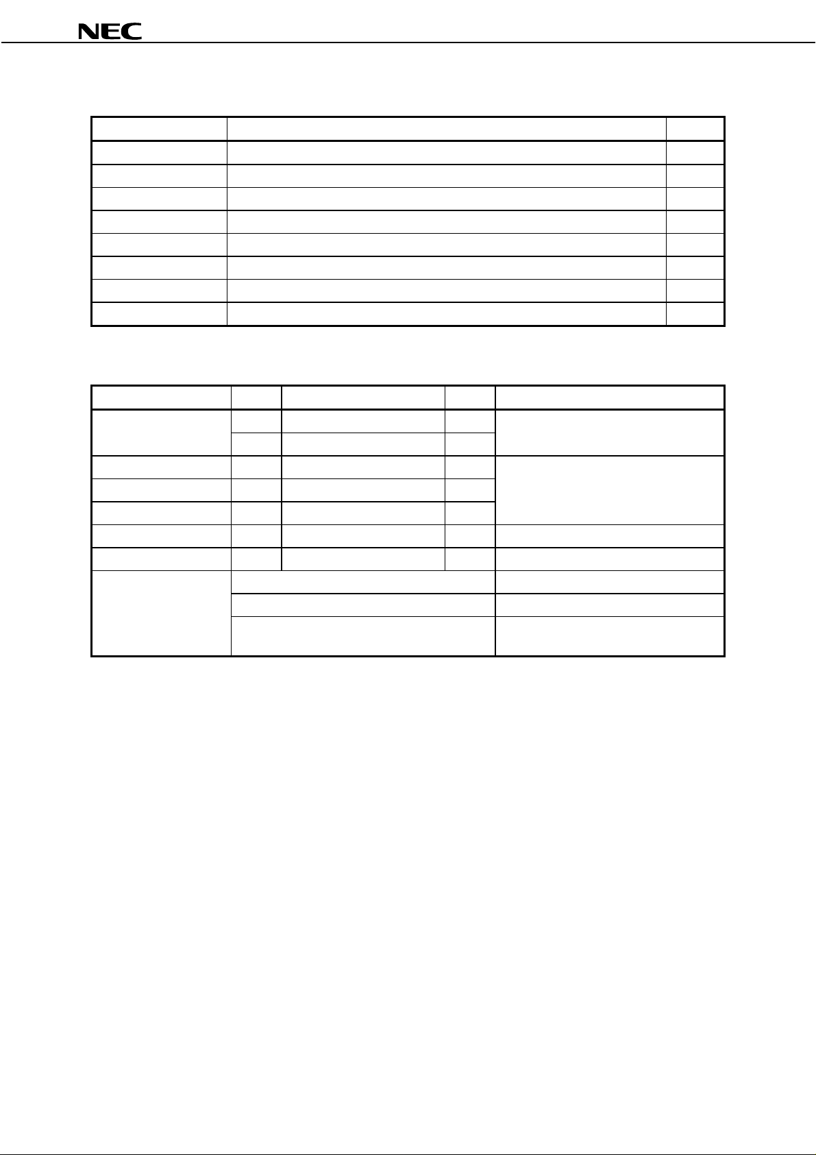
OUTLINE OF CHARACTERISTICS (at room temperature)
Display area 304.128 (H) × 228.096 (V) mm
Drive system a-Si TFT active matrix
Display colors Full-color
Number of pixels 1024 × 768
Pixel arrangement RGB vertical stripe
Pixel pitch 0.297 (H) × 0.297 (V) mm
Module size 350.0 (H) × 265.0 (V) × 23.0 (D) mm (typ.)
Weight 1480 g (typ.)
Contrast ratio 150:1 (typ., perpendicular)
Viewing angle (more than the contrast ratio of 10:1)
• Horizontal: 85° (typ., left side, right side)
• Vertical : 85° (typ., up side, down side)
2
(typ.)
= 2.2)
γ
Optimum grayscale perpendicular (
Polarizer pencil-hardness 3H (min., JISK5400)
Color gamut 48 % (typ., At center, To NTSC)
Response time 44 ms (typ.), “black” to “white”
Luminance 180 cd/m
Input signals Analog RGB, Vsync and HS
Backlight Edge light type: Four cold cathode fluorescent lamps with an inverter
<Replacement parts>
Inverter P/N: 150PW011
Lamp holder set P/N: 150LHS01
Supply voltage 12 V (typ.), 12 V (typ.)
Power consumption 24.7 W (typ.)
Data Sheet EN0417EJ1V0DS00
3
NL10276AC30-01A
GENERAL SPECIFICATIONS
Item Contents Unit
Module size 350.0 ± 0.6 (H) × 265.0 ± 0.6 (V) × 24.0 (max.) (D) mm
Display area 304.128 (H) × 228.096 (V) mm
Number of dots 1024 × 3 (H) × 768 (V) dots
Pixel pitch 0.297 (H) × 0.297 (V) mm
Dot pitch 0.099 (H) × 0.297 (V) mm
Pixel arrangement RGB (Red, Green, Blue) vertical stripe –
Display colors Full color color
Weight 1,480 (typ.), 1600 (max.) g
ABSOLUTE MAXIMUM RATINGS
Parameter Symbol Rating Unit Remarks
DD
V
DD
B –0.3 to + 14 V
V
–0.3 to + 14 VSupply voltage
Logic input voltage VIN1 –0.3 to + 5.5 V
R, G, B input voltage VIN2 –6.0 to + 6.0 V
CLK input voltage VIN3 –7.0 to + 7.0 V
Storage temp. T
Operating temp. T
Humidity
(no condensation)
ST
OP
–20 to + 60 °C –
0 to 50 °C
≤
95% relative humidity Ta ≤ 40°C
≤
85% relative humidity 40 < Ta ≤ 50°C
Absolute humidity shall not exceed Ta = 50°C,
85% relative humidity level.
Notes 1.
Measured at the LCD panel (Include own fever)
No condensation
2.
Ta = 25°C
Ta = 25°C
DD
= 12 V
V
Module surface
Ta > 50°C
Note 1
4
Data Sheet EN0417EJ1V0DS00
ELECTRICAL CHARACTERISTICS
(1) Logic, LCD driving, Backlight
Item Symbol Min. Typ. Max. Unit Remarks
DD
V
DD
B 11.4 12.0 12.6 V Backl i ght
V
Logic input “L” voltage V
Logic input “H” voltage V
iL
iH
Logic output “L” voltage VOL1 – – 0.4 V
Logic output “H” voltage VOH1 2.4 – – V
Logic input “L” current 1 I
Logic input “H” current 1 I
Logic output “L” current 1 I
Logic output “H” current 1 I
Supply current
iL1
iH1
oL1
oH1
DD
I
(Dot-checked pattern)
DD
B
I
11.4 12.0 12.6 V Logic and LCD drivingSupply voltage
0–0.8V
2.2 – 5.25 V
–1 – –
––1
––1
–1 – –
– 660 850 mA
– 45 65 mA Power saving mode
– 1400 1600 mA VDDB = 12.0 V
– 1 10 mA Power saving mode
HS/CS, Vsync, SEL, UP, DOWN,
RESET, VOLSEL, DDCCLK,
DDCDAT, OSDSEL, WPRT
LED00/01/02/10/11/12
µ
µ
µ
µ
HS/CS, Vsync
A
A
DDCDAT
A
A
V
V
(Max. luminance)
V
NL10276AC30-01A
(Ta = 25°C)
DD
= 12.0 V
DD
= 12.0 V
DD
B = 12.0 V
Note1
Note1
Pixel checkered pattern
Note
(2) Video signal (R, G, B) input
Item Min. Typ. Max. Unit Remarks
Maximum amplitude (white - black)
DC input level (black)
0
(black)
−
0.5 – +2.5 V –
0.7
(white)
*A Vp-p
Sync level 0.2 0.3 *B Vp-p G terminal
*A + *B
Note
Need to adjust contrast if the input level is beyond 0.7 Vp-p.
– – 1.1 Vp-p
Note
(sync on green)
(Ta = 25°C)
Data Sheet EN0417EJ1V0DS00
5
NL10276AC30-01A
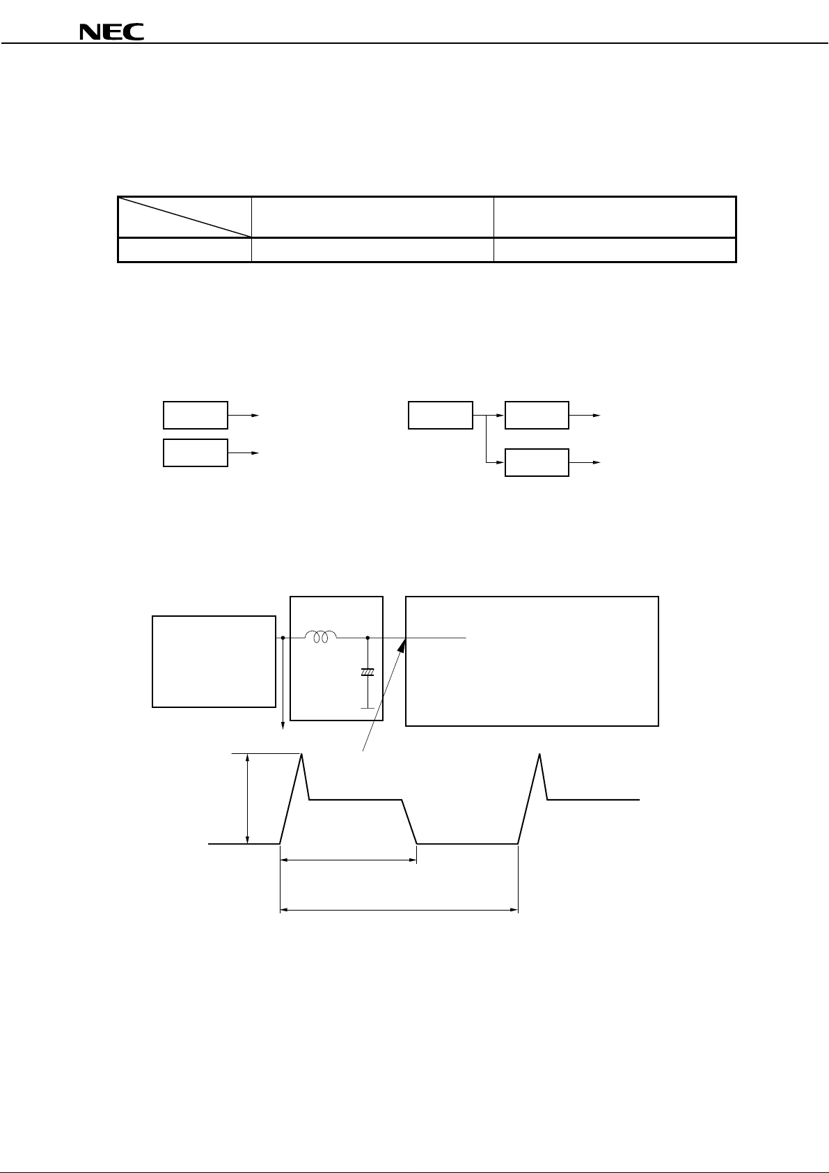
POWER SUPPLY DESIGN
(1) Ripple voltage of the supply voltage
Please note that the ripple at the input connector of the module should be within the values shown in this table.
If the ripple would be beyond these values, the noise might appear on the screen.
Acceptable range
The acceptable range of ripple voltage includes spike noises.
Note
DD
V
(for logic and LCD driver)
≤
100 mVp-p
DD
V
B
(for backlight)
≤
200 mVp-p
Example of the power supply connection to minimize the ripple voltage
a) Separate the power supply b) Put the filter
Power V
Power VDDB
DD
Power
Filter V
Filter VDDB
DD
(2) Current wave in the luminance control mode
In the luminance control mode, the rush current below flows into the inverter of the module. The duty cycle
varies from 100% through 20% depending on the luminance control level. This might cause the noise on the
screen. Please evaluate the appropriate value of the capacitor in the filter to eliminate the noise.
Filter Inverter circuit of NL10276AC30-01A
Customer’s power
supply
(12 V)
To V
Rush
current
GND
DD
*Frequency:
Vsync frequency × K*
Duty
Frequency*
*Vsync ≤ 75 Hz: K = 4.6
> 75 Hz: K = 3.6
6
Data Sheet EN0417EJ1V0DS00
NL10276AC30-01A
POWER SUPPLY SEQUENCE
There is no sequence among the synchronous signals, the video signals and the power supply. However, 12 V
for backlight should be started up within 80 ms, otherwise, the protection circuit makes the backlight turns off.
Please note that the supply voltage must not be applied while the control signals (SEL, UP, DOWN and RESET)
are connected to GND. Otherwise the module may cause malfunctions.
If the power supply voltage is applied while SEL and RESET is connected to GND, the mode is set into NEC
factory mode. In this case, both LEDON and LEDOFF become “H”. Please do not use the module in this mode
which may write over the default value. Please turn off the power supply immediately and turn on the power while
SEL and RESET are connected to GND again. If the default value has been revised by accident, please follow the
instruction below.
<NEC factory mode>
This mode can control Brightness and Contrast and OSD position. Factory Reset function is reset all values. But
do not use the module in this mode which may write over the default values affect to the LCD internal operation.
Please turn off the power immediately and turn on the power while SEL and RESET are connected to GND again.
If the default value has been revised by accident, please select “Factory Reset” mode and press “Reset” key for
over two seconds.
Functions Control contents How to reset
Brightness Total Brightness and Sub Brightness for each RGB Press RESET key over 2 seconds
Contrast Total Contrast and Sub Contrast for each RGB Press RESET key over 2 seconds
LCD Data
Color adjust
VCO
HDTV Select
OSD position Change the OSD display position
Factory Reset Above function values is reset to factory values. Press Reset key over 2 seconds.
RESET RESET the NEC factory mode
Never select and adjust values Please go to the Factory reset.
−
−
Data Sheet EN0417EJ1V0DS00
7
INTERFACE AND PIN CONNECTION
(1) Interface signals, power supply
CN101
Part No. : 1-353119-4
Adaptable socket : 1-353068-04
Supplier : Japan AMP Ltd.
NL10276AC30-01A
Pin No. Symbol Pin No. Sym bol
1B8Vsync
2 B-GND 9 GND
3G10HS/CS
4G-GND11 GND
5 R 12 DDCCLK
6 R-GND 13 N.C.
7 GND 14 DDCDAT
N.C. (No connection) should be open.
Note
CN103
Part No. : DF14A-25P-1.25H
Adaptable socket : DF14-25S-1.25C
Supplier : HIROSE ELECTRIC CO., LTD.
Pin No. Symbol Pin No. Sym bol
1 LEDON 14 RESET
2LEDOFF15 GND
3GND16BRTVOL
4 LE D00 17 GND
5 LE D01 18 VOLSEL
6 LEDD02 19 OSDSEL
7 LE D10 20 WPRT
8 LE D11 21 N.C.
9 LE D12 22 N.C.
10 GND 23 GND
11 SEL 24 N.C.
12 UP 25 N.C.
13 DOWN
Figure from socket view
······1 2 13 14
Figure from socket view
····12 2524
N.C. (No connection)
Note
8
Data Sheet EN0417EJ1V0DS00
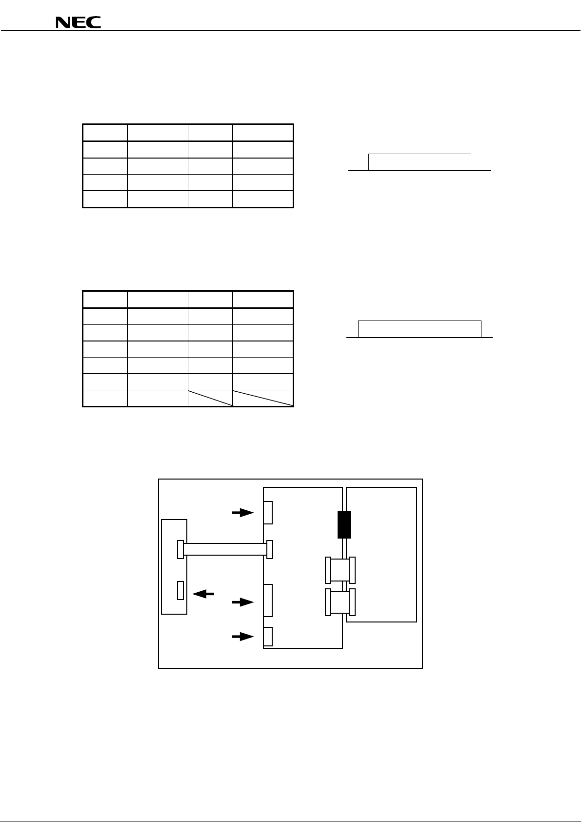
CN104
Part No. : IL-Z-8PL-SMTY
Adaptable socket : IL-Z-8S-S125C3
Supplier : Japan Aviation Electronics Industry Limited (JAE)
NL10276AC30-01A
Pin No. Symbol Pin No. Sym bol
1VDD5GND
2VDD6GND
3VDD7GND
4VDD8GND
CN201
Part No. : IL-Z-11PL1-SMTY
Adaptable socket : IL-Z-11S-S125C3
Supplier : Japan Aviation Electronics Industry Limited (JAE)
Pin No. Symbol Pin No. Sym bol
1V
2V
3V
4 GNDB 10 N.C.
5 GNDB 11 N.C.
6 GNDB
DD
B 7 N.C.
DD
B 8 N.C.
DD
B 9 N.C.
Figure from socket view
··· 12
87
Figure from socket view
·····11 10 2 1
Note
Rear view
N.C. (No connection) should be open.
CN201
1
11
1
CN101
14
1
CN103
25
8
CN104
1
Data Sheet EN0417EJ1V0DS00
9
NL10276AC30-01A
(2) Pin function
Symbol I/O Logic Description
HS/CS Input Negative Horizontal synchronous signal or composite synchronous signal (TTL level),
Positive/Negative auto recognition
Vsync I nput Negative Vertical synchronous signal (TTL level)
Positive/Negative auto recognition, Cl ock i nput f o r DDC1
R Input – Red video signal (0.7 Vp-p, 75 Ω)
G Input – Green v i deo signal (0.7 Vp-p, 75 Ω), Sync On Green input
B Input – Blue video signal (0.7 Vp-p, 75 Ω)
LEDON Output Pos itiv e Output terminal to light up LED
“H”: Power on
“L”: Power off
LEDOFF Output Positive Output terminal to light up LED
“H”: Power save mode
“L”: Normal mode
LED00 Output Positive
LED01 Output Positive
LED02 Output Positive
LED10 Output Negative
LED11 Output Negative
LED12 Output Negative
DDCCLK Input Positive CLK for DDC2B
DDCDAT Input/
Output
SEL Input Negative Select signal for control functions (TTL level)
UP Input Negative Control si gnal (TTL level)
DOWN Input Negative Control signal (TTL level)
RESET Input Negative Control signal (TTL level)
BRTVOL Input – Luminance control terminal
VOLSEL Input – Luminance control select signal (TTL level)
OSDSEL Input –
WPRT Input Positive S elect signal for DDC
Positive Data fo r DDC1/ 2B
For details, see Equivalent circuit for LED and CONTROL FUNCTIONS
Read/write
“open”: SEL off, “L”: SEL on
For details, see
UP increases the value of the functions selected.
“open”: UP off, “L”: UP on
DOWN reduces the value of the functions selected.
“open”: DOWN off, “L”: DOWN on
RESET initializes the selected functions.
“open”: RESET off “L”: RESET on
For details, see.
VOLSEL is pulled up in the module.
For details, see
Display select signal (TTL level)
“open”: OSD display off (light on LED)
“L”: OSD display on (light off LED)
For details, see
“Open”: Reading mode, “L”: Writing mode
CONTROL FUNCTIONS
Luminance control select
Luminance control select
CONTROL FUNCTIONS
10
Data Sheet EN0417EJ1V0DS00
 Loading...