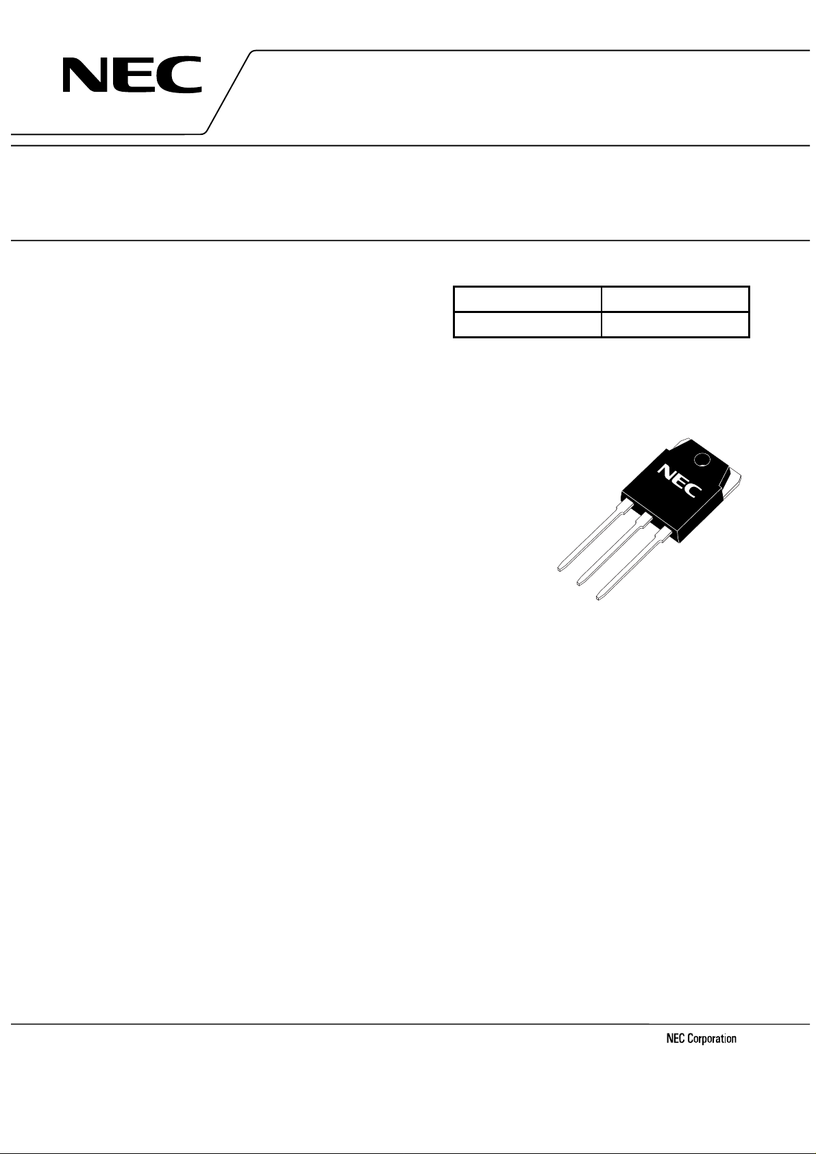
NEC 2SK3304 Datasheet

DATA SHEET
MOS FIELD EFFECT TRANSISTOR
SWITCHING
N-CHANNEL POWER MOS FET
INDUSTRIAL USE
2SK3304
DESCRIPTION
The 2SK3304 is N-Channel MOS FET device that features a
Low gate charge and excellent switching characteristics, and
designed for high voltage applications such as switching
power supply.
FEATURES
• Low gate charge :
QG = 44 nC TYP. (VDD = 450 V, VGS = 10 V, ID = 7.0 A)
• Gate voltage rating : ±30 V
• Low on-state resistance :
DS(on)
R
= 2.0 Ω MAX. (VGS = 10 V, ID = 4.0 A)
• Avalanche capability ratings
ABSOLUTE MAXIMUM RATINGS (TA = 25 °C)
Drain to Source Voltage V
Gate to Source Voltage V
Drain Current (DC) I
Drain Current (Pulse)
Total Power Dissipation (T
Total Power Dissipation (T
Note1
C
= 25°C) P
A
= 25°C) P
Storage Temperature T
Single Avalanche Current
Single Avalanche Energy
Note2
Note2
DSS
GSS(AC)
D(DC)
D(pulse)
I
stg
AS
I
AS
E
T
T
–55 to + 150 °C
ORDERING INFORMATION
PART NUMBER PACKAGE
2SK3304
900 V
±30 V
±7 A
±21 A
130 W
3.0 W
7A
147 mJ
TO-3P
(TO-3P)
Notes 1.
Document No. D13992EJ1V0DS00 (1st edition)
Date Published June 2000 NS CP(K)
Printed in Japan
PW ≤ 10
2.
Starting T
µ
s, Duty cycle ≤ 1 %
ch
= 25°C, VDD = 150 V, RG = 25 Ω, VGS = 20 V → 0 V
The information in this document is subject to change without notice. Before using this document, please
confirm that this is the latest version.
Not all devices/types available in every country. Please check with local NEC representative for
availability and additional information.
©
2000

ELECTRICAL CHARACTERISTICS (TA = 25 °C)
CHARACTERISTICS SYMBOL TEST CONDITIONS MIN. TYP. MAX. UNIT
2SK3304
Drain Leakage Current I
Gate to Source Leakage Current I
Gate to Source Cut-off Voltage V
DSS
VDS = 900 V, VGS = 0 V 100
GSS
VGS = ±30 V, VDS = 0 V ±100 nA
GS(off)VDS
= 10 V, ID = 1.0 mA 2.5 3.5 V
Forward Transfer Admittance | yfs |VDS = 20 V, ID = 4.0 A 2.5 4.7 S
Drain to Source On-state Resi stance R
Input Capacitance C
Output Capacitance C
Reverse Transfer Capacitance C
Turn-on Delay Time t
Rise Time t
Turn-off Delay Time t
Fall Time t
Total Gate Charge Q
Gate to Source Charge Q
Gate to Drain Charge Q
Body Diode Forward Voltage V
Reverse Recovery Time t
Reverse Recovery Charge Q
DS(on)VGS
iss
VDS = 10 V
V
oss
f = 1 MHz
rss
d(on)
VDD = 150 V
D
I
r
V
d(off)
R
f
G
VDD = 450 V
V
GS
D
I
GD
F(S-D) IF
rr
IF = 7.0 A, VGS = 0 V
di/dt = 50 A/
rr
= 10 V, ID = 4.0 A 1.6 2.0
1300 pF
GS
= 0 V
240 pF
55 pF
20 ns
= 4.0 A
GS(on)
= 10 V
G
= 10
RL ≅ 36
Ω,
Ω
44 ns
73 ns
45 ns
44 nC
GS
= 10 V
= 7.0 A
6nC
28 nC
= 7.0 A, VGS = 0 V 1.0 V
2.4
s
µ
13.5
A
µ
Ω
s
µ
C
µ
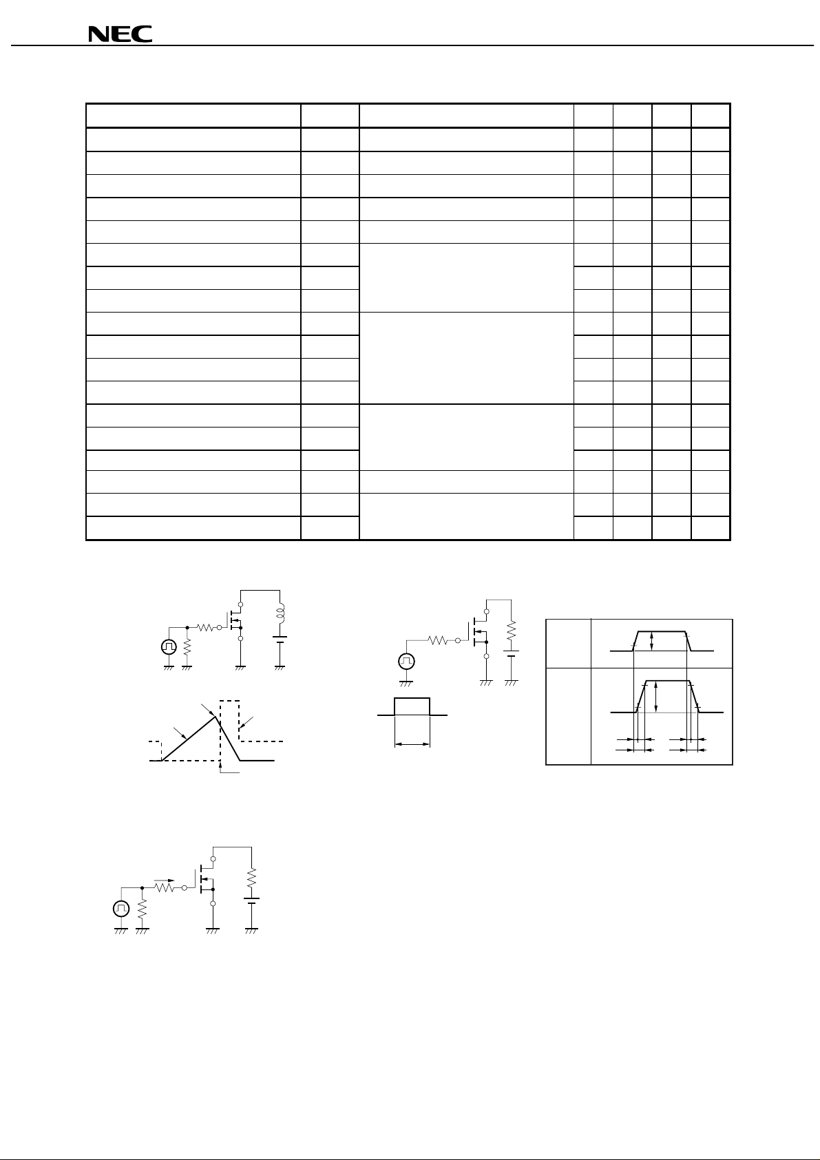
TEST CIRCUIT 1 AVALANCHE CAPABILITY
D.U.T.
L
V
DD
PG.
RG = 25 Ω
50 Ω
VGS = 20 → 0 V
BV
DSS
I
AS
V
I
D
V
DD
DS
Starting T
ch
TEST CIRCUIT 3 GATE CHARGE
D.U.T.
PG.
IG = 2 mA
50 Ω
R
L
V
DD
TEST CIRCUIT 2 SWITCHING TIME
D.U.T.
L
R
G
PG.
GS
V
0
τ = 1 s
Duty Cycle ≤ 1 %
R
V
DD
τ
µ
GS
V
Wave Form
I
D
Wave Form
V
GS
10 %
0
90 %
I
D
10 %
0
t
d(on)
r
t
on
t
90 %
V
GS
(on)
90 %
I
D
10 %
t
d(off)
t
f
t
off
2
Data Sheet D13992EJ1V0DS00

TYPICAL CHARACTERISTICS (TA = 25 °C)
2SK3304
DERATING FACTOR OF FORWARD BIAS
SAFE OPERATING AREA
100
80
60
40
20
dT - Percentage of Rated Power - %
0
20 40 60 80 100 120 140 160
C
- Case Temperature - °C
T
FORWARD BIAS SAFE OPERATING AREA
100
I
D(pulse)
I
D(DC)
=
10
DS(on)
R
(at V
1
- Drain Current - A
D
I
TC = 25
Single Pulse
0.1
1 10 1000100
7 A
Limited
= 10 V)
GS
Power Dissipation Limited
˚C
DS
- Drain to Source Voltage - V
V
100
= 21 A
10
ms
ms
TOTAL POWER DISSIPATION vs.
CASE TEMPERATURE
140
120
100
80
60
40
- Total Power Dissipation - W
T
20
P
0
20 40 60 80 100 120 140 160
C
- Case Temperature - °C
T
DRAIN CURRENT vs.
DRAIN TO SOURCE VOLTAGE
10
P
W
=100
µs
1
ms
8
6
VGS =
20 V
VGS =
10 V
VGS =
6 V
4
- Drain Current - A
D
I
2
Pulsed
0
4
DS
V
8
- Drain to Source Voltage - V
16 20
12
FORWARD TRANSFER CHARACTERISTICS
100
TA = 125˚C
10
75˚C
25˚C
−25˚C
1
- Drain Current - A
D
I
0.1
0.01
01015
5
GS
- Gate to Source Voltage - V
V
Pulsed
Data Sheet D13992EJ1V0DS00
3
 Loading...