

NEC 2SK2488 Datasheet
DATA SHEET
MOS FIELD EFFECT TRANSISTOR
SWITCHING
N-CHANNEL POWER MOS FET
INDUSTRIAL USE
DESCRIPTION
The 2SK2488 is N-Channel MOS Field Effect Transistor designed
for high voltage switching applications.
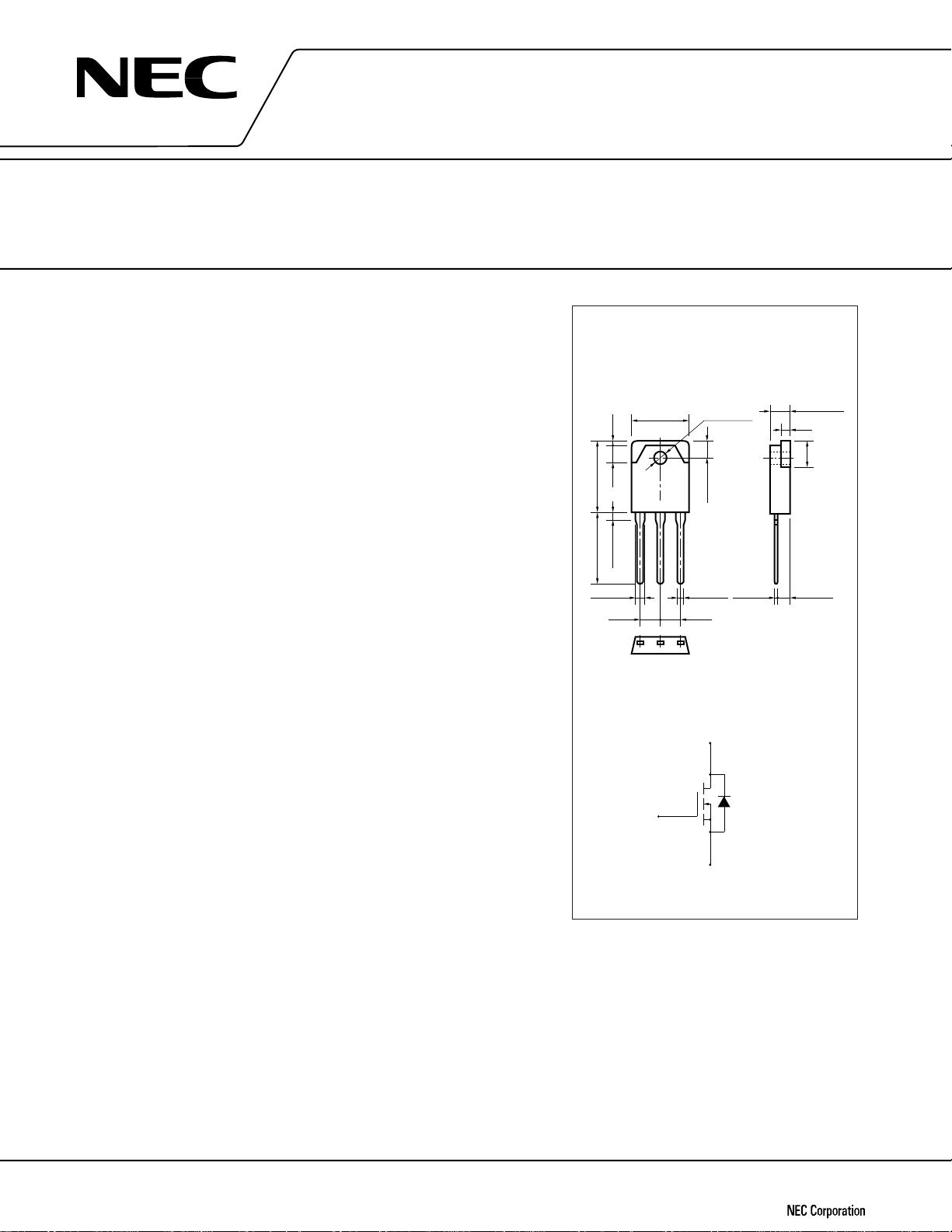
2SK2488
PACKAGE DIMENSIONS
(in millimeter)
FEATURES
• Low On-Resistance
RDS (on) = 1.2 Ω (VGS = 10 V, ID = 5.0 A)
• Low Ciss Ciss = 2 900 pF TYP.
• High Avalanche Capability Ratings
ABSOLUTE MAXIMUM RATINGS (TA = 25 ˚C)
Drain to Source Voltage
Gate to Source Voltage VGSS ±30 V
Drain Current (DC) I
Drain Current (pulse)* ID (pulse) ±20 A
Total Power Dissipation (Tc = 25 ˚C) PT1 150 W
Total Power Dissipation (TA = 25 ˚C) PT2 3.0 W
Channel Temperature T
Storage Temperature Tstg –55 to +150 ˚C
Single Avalanche Current** IAS 10 A
Single Avalanche Energy** E
* PW ≤ 10 µs, Duty Cycle ≤ 1 %
** Starting Tch = 25 ˚C, RG = 25 Ω, VGS = 20 V → 0
VDSS 900 V
D (DC) ±10 A
ch 150 ˚C
AS 294 mJ
15.7 MAX.
1.06.0
123
19 MIN. 20.0±0.2
3.0±0.2
5.45 5.45
Gate
4
1.0±0.2
MP-88
Drain
3.2±0.2
4.5±0.2
1. Gate
2. Drain
3. Source
4. Fin (Drain)
Body
Diode
4.7 MAX.
1.5
7.0
2.8±0.10.6±0.12.2±0.2
Document No. D10284EJ1V0DS00 (1st edition)
Date Published August 1995 P
Printed in Japan
Source
©
1995
ELECTRICAL CHARACTERISTICS (TA = 25 ˚C)
2SK2488
CHARACTERISTIC SYMBOL MIN. TYP. MAX. TEST CONDITIONS
Drain to Source On-Resistance RDS (on) 1.0 1.2 VGS = 10 V, ID = 5.0 A
Gate to Source Cutoff Voltage VGS (off) 2.5 3.5 VDS = 10 V, ID = 1 mA
Forward Transfer Admittance | yfs | 3.5 VDS = 20 V, ID = 5.0 A
Drain Leakage Current IDSS 100 VDS = VDSS, VGS = 0
Gate to Source Leakage Current IGSS ±100 VGS = ±30 V, VDS = 0
Input Capacitance Ciss 2 900 VDS = 10 V
Output Capacitance Coss 400 VGS = 0
Reverse Transfer Capacitance Crss 70 f = 1 MHz
Turn-On Delay Time td (on) 35 ID = 5.0 A
Rise Time tr 30 VGS = 10 V
Turn-Off Delay Time td (off) 160 VDD = 150 V
Fall Time tf 32
Total Gate Charge QG 90 ID = 10 A
Gate to Source Charge QGS 16 VDD = 450 V
Gate to Drain Charge QGD 40 VGS = 10 V
Body Diode Forward Voltage VF (S-D) 1.0 IF = 10 A, VGS = 0
Reverse Recovery Time trr 990 IF = 10 A, VGS = 0
Reverse Recovery Charge Qrr 7.0 di/dt = 50 A/µs
UNIT
Ω
V
S
µ
A
nA
pF
pF
pF
ns
ns
ns
ns
nC
nC
nC
V
ns
µ
C
R
= 10 Ω
G
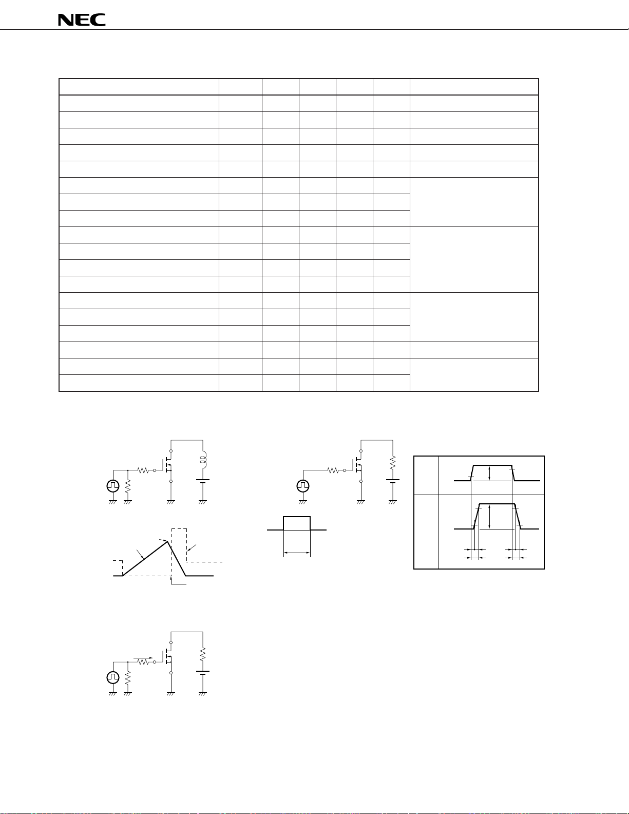
Test Circuit 1 Avalanche Capability
D.U.T.
R
G = 25 Ω
PG
VGS = 20 - 0 V
50 Ω
BVDSS
IAS
ID
VDS
VDD
Starting Tch
Test Circuit 3 Gate Charge
D.U.T.
I
G = 2 mA
PG.
50
Ω
L
V
RL
VDD
Test Circuit 2 Switching Time
D.U.T.
L
R
DD
PG.
RG
G = 10 Ω
R
VDD
VGS
0
t
t = 1 us
Duty Cycle ≤ 1 %
VGS
Wave Form
ID
Wave Form
VGS
10 %
0
ID
90 %
10 %
0
td (on) tr td (off) tf
ton toff
90 %
GS (on)
V
90 %
ID
10 %
The application circuits and their parameters are for references only and are not intended for use in actual design-in's.
2

TYPICAL CHARACTERISTICS (TA = 25 ˚C)
g
2SK2488
DERATING FACTOR OF FORWARD BIAS
SAFE OPERATING AREA
100
80
60
40
20
dT - Percentage of Rated Power - %
0
20 40 60 80 100 120 140 160
T
C - Case Temperature - ˚C
FORWARD BIAS SAFE OPERATING AREA
100
ID(pulse)
10
R
DS (on)
ID(DC)
Limited
Power Dissipation Limited
PW=100 s
10 ms
100 ms
1 ms
TOTAL POWER DISSIPATION vs.
CASE TEMPERATURE
210
180
150
120
90
60
30
PT - Total Power Dissipation - W
0
20 40 60 80 100 120 140 160
T
C - Case Temperature - ˚C
DRAIN CURRENT vs.
DRAIN TO SOURCE VOLTAGE
Pulsed
µ
20
VGS = 20 V
10 V
8 V
6 V
1
ID - Drain Current - A
TC = 25 ˚C
Single Pulse
1
1
10 100 1000
V
DS - Drain to Source Voltage - V
FORWARD TRANSFER CHARACTERISTICS
100
TA = –25 ˚C
25 ˚C
75 ˚C
10
125 ˚C
1.0
ID - Drain Current - A
0.1
0
510 15
GS - Gate to Source Volta
V
e - V
Pulsed
VDS = 10 V
10
ID - Drain Current - A
0
V
DS - Drain to Source Voltage - V
10
20
30
40
3
 Loading...