

NATIONAL SEMICONDUCTOR USBN9602-28MX, USBN9602-28M Datasheet
USBN9602 (Universal Serial Bus) Full Speed Function Controller With DMA Support
© 1998 National Semiconductor Corporation
www.national.com
November 1998
USBN9602 (Universal Serial Bus)
Full Speed Function Controller With DMA Support
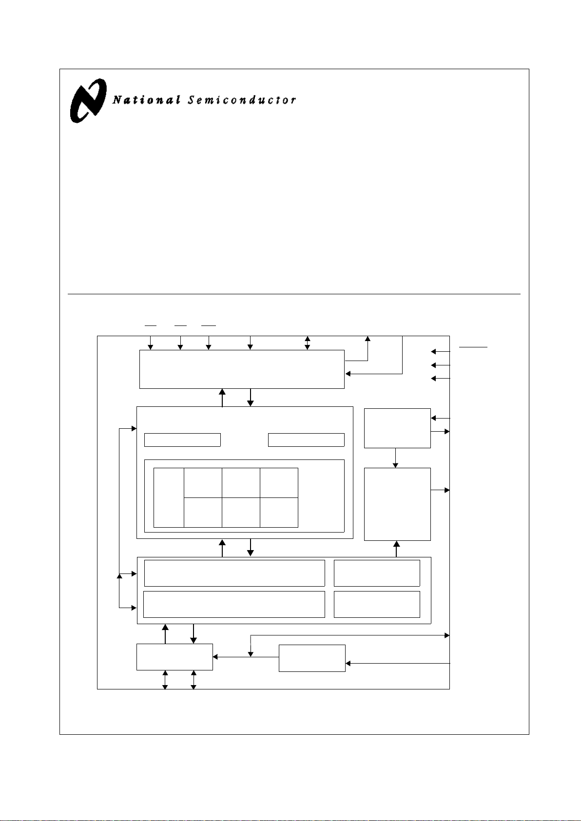
1.0 General Description
The USBN9602 is an integrated USB Node controller compatible with the USB Specification Versions 1.0 and 1.1.
Integrated onto a single IC are the required USB transceiver with a 3.3V Regulator, Media Access Controller,
USB endpoint (EP) FIFOs, a versatile 8-bit parallel interface, MICROWIRE/PLUS™ Interface and a clock generator. A total of seven FIFO buffers support the different USB
messages: one bidirectional FIFO for the mandatory con-
Block Diagram
TRI-STATE® is a registered trademark of National Semiconductor Corporation.
MICROWIRE/PLUS
™ and MICROWIRE™ are trademarks of National Semiconductor Corporation.
Physical Layer Interface (PHY)
Media Access Controller (MAC)
Transceiver
48 MHz
Oscillator
Clock
Generator
XIN
XOUT
CLKOUT
Microcontroller Interface
D+
D-
Upstream Port
INTR
V3.3
CS RD WR A0/ALE D[7:0]/AD[7:0]
EP2
Endpoint0
EP1
EP6EP5
RX
TX
Endpoint/Control FIFOs
VReg
AGND
RESET
Vcc
GND
MODE[1:0]
StatusControl
SIE
USB Event
Detect
Clock
Recovery
EP4EP3
trol endpoint EP0 and six FIFOs for an additional six unidirectional Endpoint Pipes to support USB interrupt, bulk and
isochronous data transfers. The 8-bit parallel interface supports multiplexed and non-multiplexed style CPU
address/data buses. A programmable interrupt output
scheme allows device configuration for different interrupt
signaling requirements.

2 www.national.com
2.0 Features
■ Full-Speed USB Node Device
■ USB transceiver
■ 3.3V signal voltage regulator
■ 48 MHz oscillator circuit
■ Programmable clock generator
■ Serial Interface Engine consisting of Physical Layer In-
terface (PHY) and Media Access Controller (MAC), USB
Specification 1.0 compliant
■ Control/Status Register File
■ USB Function Controller with seven FIFO-based End-
points:
– One bidirectional Control Endpoint 0 (8 bytes)
– Three Transmit Endpoints (2*32 and 1*64 bytes)
– Three Receive Endpoints (2*32 and 1*64 bytes)
■ 8-bit parallel interface with two selectable modes:
– non-multiplexed
– multiplexed (Intel compatible)
■ DMA support for parallel interface
■ MICROWIRE/PLUS™ Interface
■ 28-pin SO package

3 www.national.com
Table of Contents
1.0 General Description . . . . . . . . . . . . . . . . . . . . . . . . . . . .1
2.0 Features . . . . . . . . . . . . . . . . . . . . . . . . . . . . . . . . . . . . . .2
3.0 Device Overview . . . . . . . . . . . . . . . . . . . . . . . . . . . . . . . 4
3.1 Transceiver . . . . . . . . . . . . . . . . . . . . . . . . . . . . . .4
3.2 Voltage Regulator (VReg) . . . . . . . . . . . . . . . . . . . 4
3.3 Serial Interface Engine (SIE) . . . . . . . . . . . . . . . . . 4
3.4 Endpoint/Control FIFOs . . . . . . . . . . . . . . . . . . . . .4
3.5 Microcontroller Interface . . . . . . . . . . . . . . . . . . . . 5
4.0 Connection Diagram . . . . . . . . . . . . . . . . . . . . . . . . . . .5
5.0 Pin Descriptions . . . . . . . . . . . . . . . . . . . . . . . . . . . . . . .6
6.0 Parallel Interface . . . . . . . . . . . . . . . . . . . . . . . . . . . . . . . 9
6.1 Non-Multiplexed Mode . . . . . . . . . . . . . . . . . . . . . . 9
6.2 Multiplexed Mode . . . . . . . . . . . . . . . . . . . . . . . . . 10
7.0 DMA Support . . . . . . . . . . . . . . . . . . . . . . . . . . . . . . . . . 12
8.0 MICROWIRE/PLUS Interface . . . . . . . . . . . . . . . . . . . . 13
9.0 Device Functional States . . . . . . . . . . . . . . . . . . . . . . . 16
9.1 Suspend Operation . . . . . . . . . . . . . . . . . . . . . . . 16
9.2 Remote Resume . . . . . . . . . . . . . . . . . . . . . . . . .16
9.3 USB Resume Operation . . . . . . . . . . . . . . . . . . . 16
9.4 Functional State Transitions . . . . . . . . . . . . . . . . 16
10.0 Endpoint Operation . . . . . . . . . . . . . . . . . . . . . . . . . . .18
10.1 Transmit and Receive Endpoint FIFOs . . . . . . . . 18
10.2 Bidirectional Control Endpoint FIFO0 Operation .19
10.3 Transmit Endpoint FIFO Operation (TXFIFO1,
TXFIFO2, TXFIFO3) . . . . . . . . . . . . . . . . . . . . . . 19
10.4 Receive Endpoint FIFO Operation (RXFIFO1,
RXFIFO2, RXFIFO3) . . . . . . . . . . . . . . . . . . . . . . 20
10.5 Programming Model . . . . . . . . . . . . . . . . . . . . . .21
11.0 Register Set . . . . . . . . . . . . . . . . . . . . . . . . . . . . . . . . . . 23
11.1 Main Control Register (MCNTRL) . . . . . . . . . . . . 23
11.2 Clock Configuration Register (CCONF) . . . . . . . . 23
11.3 DMA Control Register (DMACNTRL) . . . . . . . . .24
11.4 Revision Identifier Register (RID)Revision Identifier (RID)
24
11.5 Node Functional State Register (NFSR) . . . . . . . 24
11.6 Main Event Register (MAEV) . . . . . . . . . . . . . . . .25
11.7 Main Mask Register (MAMSK) . . . . . . . . . . . . . .25
11.8 Alternate Event Register (ALTEV) . . . . . . . . . . . .25
11.9 Alternate Mask Register (ALTMSK) . . . . . . . . . . . 26
11.10 Transmit Event Register (TXEV) . . . . . . . . . . . . .26
11.11 Transmit Mask Register (TXMSK) . . . . . . . . . . . 26
11.12 Receive Event Register (RXEV) . . . . . . . . . . . . . 27
11.13 Receive Mask Register (RXMSK) . . . . . . . . . . . 27
11.14 NAK Event Register (NAKEV) . . . . . . . . . . . . . . 27
11.15 NAK Mask Register (NAKMSK) . . . . . . . . . . . . . 27
11.16 FIFO Warning Event Register (FWEV) . . . . . . . . 27
11.17 FIFO Warning Mask Register (FWMSK) . . . . . . 28
11.18 Frame Number High Byte Register (FNH) . . . . . 28
11.19 Frame Number Low Byte Register (FNL) . . . . . . 28
11.20 Function Address Register (FAR) . . . . . . . . . . . . 28
11.21 Endpoint Control Register 0 (EPC0) . . . . . . . . . . 29
11.22 Transmit Status Register 0 (TXS0) . . . . . . . . . . . 29
11.23 Transmit Command Register 0 (TXC0) . . . . . . . 29
11.24 Transmit Data Register 0 (TXD0) . . . . . . . . . . . . 30
11.25 Receive Status Register 0 (RXS0) . . . . . . . . . . . 30
11.26 Receive Command Register 0 (RXC0) . . . . . . . . 30
11.27 Receive Data Register 0 (RXD0) . . . . . . . . . . . . 31
11.28 Endpoint Control Register x (EPC1 through
EPC6) . . . . . . . . . . . . . . . . . . . . . . . . . . . . . . . . . 31
11.29 Transmit Status Register x (TXS1, TXS2, TXS3) 31
11.30 Transmit Command Register x (TXC1, TXC2, TXC3)
32
11.31 Transmit Data Register x (TXD1, TXD2, TXD3) . 32
11.32 Receive Status Register x (RXS1, RXS2, RXS3) 33
11.33 Receive Command Register x (RXC1, RXC2, RXC3)
33
11.34 Receive Data Register x (RXD1, RXD2, RXD3) . 34
12.0 Design considerations . . . . . . . . . . . . . . . . . . . . . . . . 35
12.1 Targeted Applications . . . . . . . . . . . . . . . . . . . . . 35
12.2 3.3V Regulator Issues . . . . . . . . . . . . . . . . . . . . 35
12.3 Simplified Application Diagrams . . . . . . . . . . . . . 35
13.0 Memory Map . . . . . . . . . . . . . . . . . . . . . . . . . . . . . . . . 36
14.0 Electrical Characteristics - PRELIMINARY . . . . . . . . 37
14.1 Parallel Interface Timing (MODE[1:0] = 00b) . . . 39
14.2 Parallel Interface Timing (MODE[1:0] = 01b) . . . 41
14.3 DMA Support Timing . . . . . . . . . . . . . . . . . . . . . 43
14.4 MICROWIRE Interface Timing
(MODE[1:0] = 10b) . . . . . . . . . . . . . . . . . . . . . . . 44
15.0 Physical Dimensions . . . . . . . . . . . . . . . . . . . . . . . . . 45

4 www.national.com
3.0 Device Overview
The USBN9602 is an integrated USB Node controller. The
block diagram on page 1 of the data sheet shows the major on-chip components of the device.
3.1 Transceiver
The USBN9602 contains a high-speed transceiver, which
consists of three main functional blocks:
– differential receiver
– single-ended receiver with on-chip voltage reference
– transmitter with on-chip current source
The performance requirements met by this transceiver are
described in Chapter 7 of the Universal Serial Bus Speci-
fication Version 1.0.
To minimize signal skew, the differential output swings of
the transmitter are well balanced. Slew-rate control is
used on the driver to minimize radiated noise and cross
talk. The drivers support TRI-STATE® operation to allow
bidirectional half-duplex operation of the transceiver.
The differential receiver operates over the complete common mode range, that is guaranteed to be larger than that
of the single-ended receivers, to avoid potential glitches in
the Serial Interface Engine (SIE) after Single-Ended Zeros.
Single-ended receivers are present on each of the two
data lines. These are required, in addition to the differential receiver, to detect an absolute voltage with a switching
threshold between 0.8V and 2.0V (TTL inputs). An external 1.5
± 5% kΩ resistor, tied to a voltage source between
3.0V and 3.6V referenced to the local ground, is required
on D+ to indicate that this is a high-speed node.
3.2 Voltage Regulator (VReg)
The Voltage Regulator provides a 3.3V voltage from the
5.0V device power for the integrated transceiver. This
3.3V output can be used to supply power to the 1.5 k
Ω
pull-up resistor. It can be disabled under software control
to allow using the device in a 3.3V system. This output
must be decoupled with a 10
µF tantalum capacitor to
ground.
3.3 Serial Interface Engine (SIE)
The USB Serial Interface Engine (SIE) consists of a Physical Layer Interface (PHY) level and a Media Access Controller (MAC) level. The PHY level includes the digitalclock recovery circuit, a digital glitch filter, End_Of_Packet
detection circuitry, and bit stuffing and unstuffing logic.
The MAC level includes packet formatting, CRC generation and checking, endpoint address detection, and provides the necessary control to give the NAK, ACK, and
STALL responses as determined by the Endpoint Controller for the specified endpoint pipe. The SIE is also responsible for detecting and reporting events on detection of
USB-specific events such as Reset, Suspend, and Resume. The transmitter outputs of the module to the transceiver are well matched (under 1 ns) to minimize skew on
the USB signals.
The USB standard specifies bit stuffing and unstuffing as
a method to ensure adequate transitions on the line to enable clock recovery at the receiving end. Whenever a
string of consecutive 1s is encountered, the bit-stuffing
logic inserts a 0 after every sixth 1 in the data stream. The
bit-unstuffing logic reverses this process.
The clock recovery block uses the incoming NRZI data to
extract a data clock (12 MHz) from an input clock derived
from a crystal or crystal oscillator (48 MHz frequency).
This clock is used in the data recovery circuit. The output
of this block is binary data (decoded from the NRZI
stream) that can be appropriately sampled using the extracted 12 MHz clock. The jitter performance and timing
characteristics meet the requirements set forth in Chapter
7 of the USB Specification.
3.4 Endpoint/Control FIFOs
The Endpoint Pipe Controller (EPC) provides the interface
for USB Function endpoints. An endpoint is the ultimate
source or sink of data. An endpoint pipe provides for the
movement of data between USB and memory, and completes the path between the USB Host and the function
endpoint. According to the USB specification, up to 31
such endpoint pipes are supported at any given time,
each with the same Function Address. The USBN9602,
however, supports a maximum of seven endpoint pipes.
A USB Function is a USB device that is able to transmit
and receive information on the bus. A Function may have
one or more configurations, each of which defines the interfaces that make up the device. Each interface, in turn,
is composed of one or more endpoints.
Each endpoint is an addressable entity on USB and is required to respond to IN and OUT tokens from the USB
Host (typically a PC). An IN token indicates that the host
has requested to receive information from an endpoint,
and an OUT token indicates that the host is about to send
information to an endpoint.
Upon detection of an IN token addressed to an endpoint,
the endpoint is responsible for responding with a data
packet. If the endpoint is currently stalled, a STALL handshake packet is sent under software control. If the endpoint is enabled, but no data is present, a NAK (Negative
Acknowledgment) handshake packet is sent automatically.
If the Endpoint is Isochronous and enabled, but no data
present, a bit stuff error followed by an end of packet is
sent on the bus.
Similarly, upon detection of an OUT token addressed to
an endpoint, the endpoint is responsible for receiving a
data packet sent by the host and storing it in a buffer. If
the endpoint pipe is currently stalled, a STALL handshake
packet is sent at the end of the data transmission. If the
endpoint pipe is currently disabled, no handshake packet
is sent at the end of the data transmission. If the endpoint
pipe is enabled, but no buffer is present in which to store
the data, a NAK (Negative Acknowledgment) handshake
packet is sent. If the Endpoint is Isochronous and enabled
but can’t handle the data, the data will be lost.
5 www.national.com
A Disabled endpoint does not respond to IN, OUT, or
SETUP tokens.
The Endpoint Pipe Controller maintains separate status
and control information for each endpoint pipe.
For IN tokens, the Endpoint Pipe Controller is responsible
for transferring data from the defined buffer to the host.
For OUT tokens, the Endpoint Pipe Controller is responsible for transferring data from the host to the defined buffer.
3.5 Microcontroller Interface
A CPU or microcontroller can be connected via an 8-bit
parallel interface or a MICROWIRE interface. For the parallel interface, there are two addressing modes (multiplexed or non-multiplexed). These modes are selected by
hardwiring the proper binary code on the MODE1 and
MODE0 pins.
In addition, an interrupt output is provided. The type of the
interrupt can be programmed to be either push-pull activehigh or active-low output, or an open-drain active-low output.
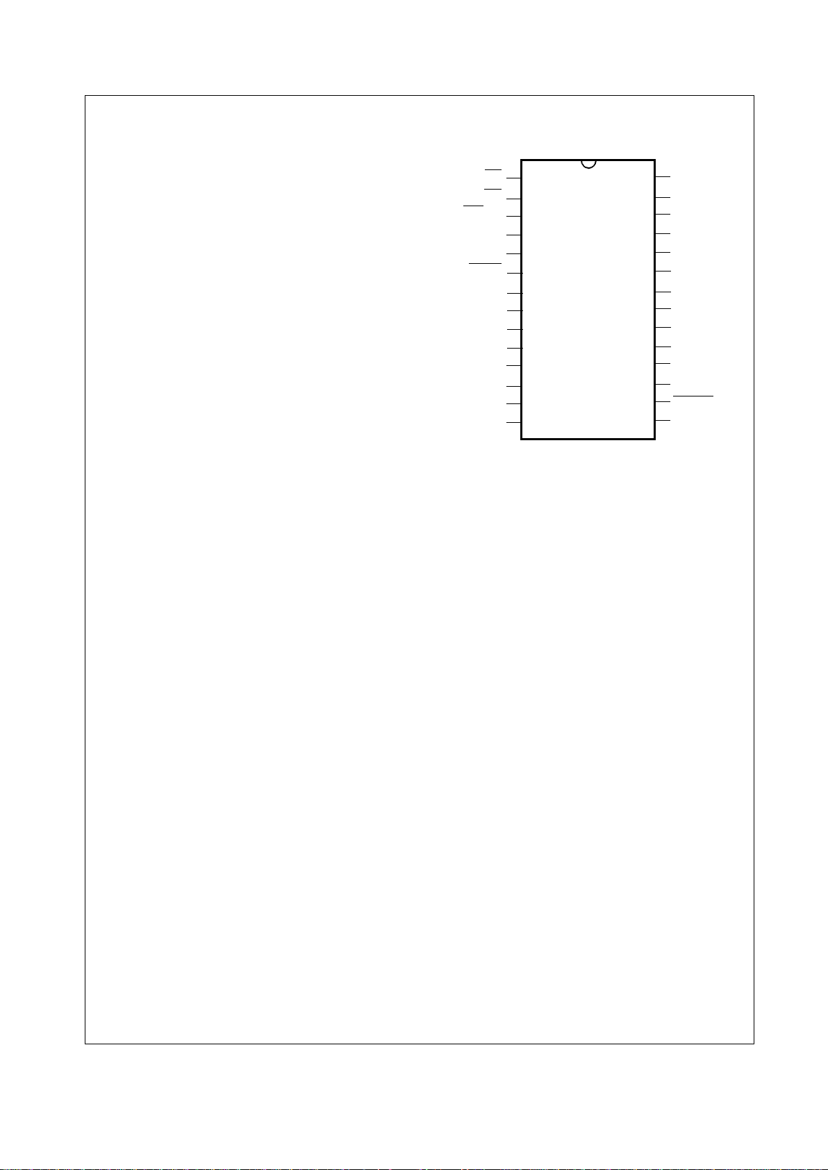
4.0 Connection Diagram
Figure1. USBN9602 Connection Diagram
CS
RD
WR/SK
DACK
GND
Vcc
GND
MODE1
MODE0
D6
D5
D4
D3
1
2
3
4
5
6
7
8
9
10
11
12
13
14
28
27
26
25
24
23
22
21
20
19
18
17
16
15
INTR
XOUT
XIN
CLKOUT
D7
AGND
D–
D+
V3.3
RESET
A0/ALE/SI
D0/SO
D1
D2
28 pin
SO
DRQ
Order Number USBN9602-28M
See NS Package Number M28B
6 www.national.com
5.0 Pin Descriptions
The following tables briefly describe the USBN9602 pins.
Each table lists a related set of device pins and shows the
device pin number, the signal direction (“I” for input, “O”
for output, “I/O” for bidirectional, or N.A. for not applica-
ble), and a brief description of the pin function.
Note that unused input or bidirectional pins must be pulled
up or down as appropriate. This is essential to reduce
overall power consumption and to limit EMI.
5.0.1 Power Supply
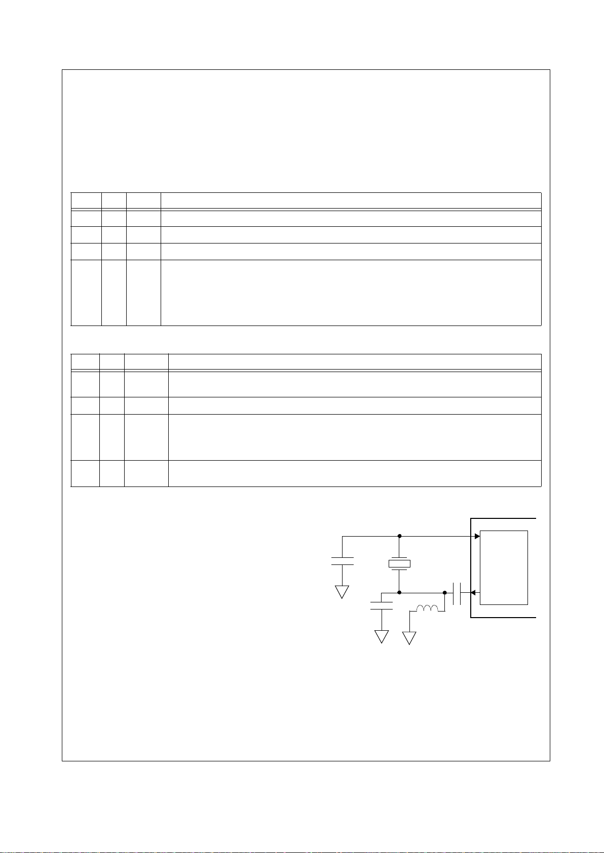
5.0.2 Oscillator, Clock and Reset
Oscillator Circuits
The XIN and XOUT pins may be connected to make a 48
MHz closed loop crystal controlled oscillator. Alternately an
external 48 MHz clock source may be input to clock the
device. The internal crystal oscillator uses a 48 MHz 3rd
harmonic crystal. The circuit for the crystal option is shown
in Figure2. If an external clock source is used, it is connected to XIN. XOUT is unconnected.
Stray capacitance and inductance should be kept as low as
possible in the oscillator circuit. Trace lengths should be
minimized by locating the crystal and external components
as close as possible to the XIN and XOUT pins.
Note: The circuit shown has been tested with crystals from
ECS Inc. only (e.g. part number ECS-480-S-1-3OT). For
other crystals , please consult the manufacturer for recommended circuit and component values.
Pin # Dir Label Pin Functional Description
22 N.A. Vcc Digital Power Supply (Vcc)
21,23 N.A. GND Digital Power Supply (GND)
17 N.A. AGND Analog Power Supply (AGND)
18 N.A. V3.3 Transceiver 3.3V Voltage Supply. This pin can be used as the internal 3.3V voltage regulator out-
put. The regulator is intended to power only the internal transceiver and one external pull-up. An
external 1
µF de-coupling capacitor is required on this pin. The voltage regulator output is dis-
abled upon hardware reset. If the internal voltage regulator is left disabled, this pin can be used
as an 3.3V supply input for the transceiver.
Pin # Dir Label Pin Functional Description
26 N.A. XIN Input for internal 48 MHz crystal oscillator circuit. A 48 MHz third harmonic crystal may be used.
27 N.A. XOUT Output for the internal crystal oscillator circuit.
28 O CLKOUT Clock Output. This pin provides a programmable clock source. Upon hardware reset, this pin
sources a 4 MHz clock (there may be an initial phase discontinuity). It may be programmed for
different speeds or disabled via the Clock Configuration Register (these subsequent transitions
are synchronous and will occur smoothly).
16 I RESET Active-Low Reset input. Signal conditioning is provided on this pin to allow the use of a simple
RC power-on reset circuit.
Figure2. 3rd Harmonic Crystal Oscillator
Connections
XTAL1
C2
C1
48 MHz
OSC
XIN
C3
L1
7 www.national.com
5.0 Pin Descriptions (Continued)
5.0.3 USB Port
Component Parameters Values Tolerance
Crystal 1 Resonance Frequency
Third Overtone
Type
Maximum Effective Series Resistance
Maximum Shunt Capacitance
Maximum Drive Level
48 MHz
Parallel
AT-Cut
40
Ω
7 pF
1 mW
2500 ppm
C1 22 pF 10%
C2 56 pF 10%
C3 100 nF 10%
L1 470 nH 10%
Pin # Dir Label Pin Functional Description
19 I/O D+ USB D+ upstream port. This pin requires an external 1.5k pull-up to 3.3V to signal full speed
operation.
20 I/O D– USB D– upstream port.
5.0 Pin Descriptions (Continued)
8 www.national.com
5.0.4 Microprocessor Interface
Pin # Dir Label Pin Functional Description
24:25 I MODE[1:0] Interface Mode select input pins. Each of these pins should be hard-wired to Vcc or GND
to select the interface mode:
MODE[1:0] = 00: Mode 0: non-multiplexed parallel interface mode
MODE[1:0] = 01: Mode 1: multiplexed parallel interface mode
MODE[1:0] = 10: Mode 2: MICROWIRE interface mode
MODE[1:0] = 11: Mode 3: reserved†
†Note: Mode 3 also selects the MICROWIRE interface mode in the USBN9602, but this
mode should be reserved to preserve compatibility with future devices.
6 I DACK
Active-low DMA Acknowledge. This pin is only used if DMA is enabled. If DMA is not used,
this pin must be tied to Vcc.
5 O DRQ DMA Request. This pin is only used if DMA is enabled.
4 O INTR Interrupt Output. The interrupt signal modes (active high, active low or open drain) can be
programmed via the Main Control Register. During Reset, this pin is placed in the TRI-
STATE mode.
1 I CS
Active-low chip select signal.
2 I RD
Active-low read signal for parallel interface.
3 I WR
Mode 0,1: Active-low write signal for parallel interface.
SK Mode 2: MICROWIRE shift clock
7 I A0 Mode 0 address bus line A0 for parallel interface.
ALE Mode 1 Address Latch Enable for parallel interface.
SI Mode 2 MICROWIRE Serial Input
8 I/O D0 Mode 0 Data bus line D0
AD0 Mode 1 Address/Data bus line AD0
SO Mode 2 MICROWIRE Serial Output
9 I/O D1 Mode 0 Data bus line D1
AD1 Mode 1 Address/Data bus line AD1
10 I/O D2 Mode 0 Data bus line D2
AD2 Mode 1 Address/Data bus line AD2
11 I/O D3 Mode 0 Data bus line D3
AD3 Mode 1 Address/Data bus line AD3
12 I/O D4 Mode 0 Data bus line D4
AD4 Mode 1 Address/Data bus line AD4
13 I/O D5 Mode 0 Data bus line D5
AD5 Mode 1 Address/Data bus line AD5
14 I/O D6 Mode 0 Data bus line D6
AD6 Mode 1 Address/Data bus line AD6
15 I/O D7 Mode 0 Data bus line D7
AD7 Mode 1 Address/Data bus line AD7
9 www.national.com
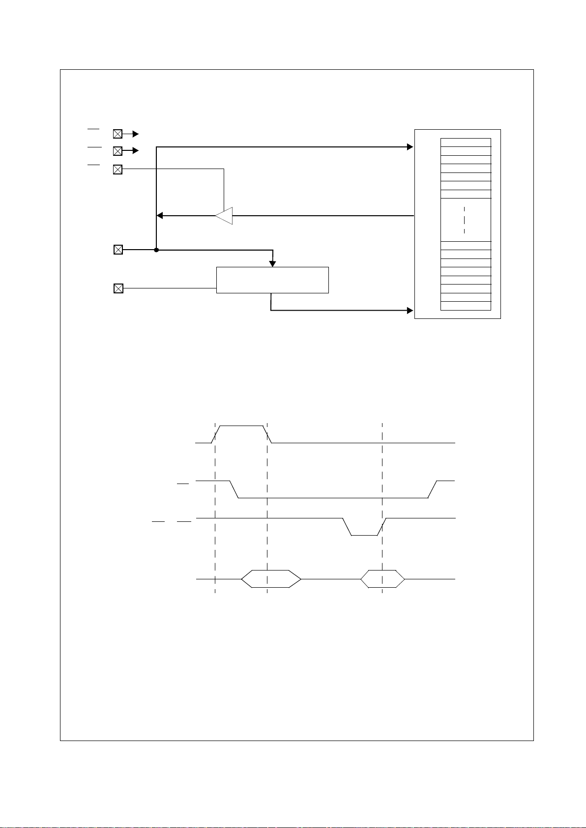
6.0 Parallel Interface
The parallel interface allows the USBN9602 to function as
a CPU or microcontroller peripheral. One of two interface
modes can be selected via the MODE0 pin while the
MODE1 pin is pulled low:
– Non-multiplexed mode
– Multiplexed mode
6.1 Non-Multiplexed Mode
The non-multiplexed mode uses the control pins CS, RD,
WR
, the address pin A0, and the bidirectional data bus
D[7:0], as shown in Figure 3. This mode is selected by tying both the MODE1 and MODE0 pin to GND.
The CPU has direct access to the registers DATA_IN,
DATA_OUT and ADDR. Reading and writing data to the
USBN9602 can be done either in standard or burst mode.
See Figure 4 for timing information on the signal timing in
non-multiplexed mode.
CS
A0
WR
0x00
0x3F
DATA_IN
D[7:0]
RD
DATA OUT
DATA IN
REGISTER FILE
DATA_OUT
ADDR
ADDRESS
Figure3. Non-Multiplexed Mode Interface Block Diagram
6.0 Parallel Interface (Continued)
10 www.national.com
6.1.1 Standard Access Mode
The standard USBN9602 access sequence for the nonmultiplexed interface mode is to write the address to the
ADDRESS register and then read or write the data from/to
the DATA_OUT/DATA_IN register. Updating of the
DATA_OUT register occurs following the write of the
ADDR register. Selection between the ADDRESS register
and the DATA_OUT/DATA_IN register is done with the A0
input.
6.1.2 Burst Mode
In burst mode, the ADDR register is written once with the
memory address of the desired on-chip register. Then
consecutive reads/writes are performed to the
DATA_OUT/DATA_IN register without writing a new address. The DATA_OUT register contents for read operations are updated once after every read.
6.1.3 User Registers
The following table gives an overview of the parallel interface registers in non-multiplexed mode. In the table, the
reserved bits return undefined data on read and should be
written with zero.
6.1.4 ADDRESS
The address register (ADDR) acts as a pointer to the internal memory. This register is write-only and is cleared
upon reset.
6.1.5 DATA_OUT
The Data Output register (DATA_OUT) is updated with the
memory register to which the ADDR register is pointing.
Update occurs under the following conditions:
1. After the ADDR register is written
2. After a read from the DATA_OUT register
3. After a write to the DATA_IN register
This register is read-only and holds undefined data after
reset.
6.1.6 DATA_IN
The Data Input register (DATA_IN) holds the data which is
written to the USBN9602 address ADDR is pointing to.
This register is write-only and is cleared upon reset.
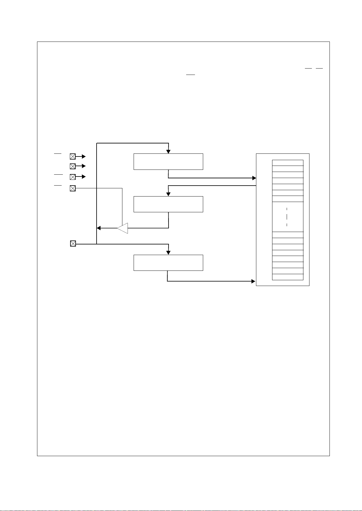
6.2 Multiplexed Mode
The multiplexed mode uses the control pins CS, RD, WR,
the address latch enable signal ALE, and the bidirectional
address data bus AD[7:0], as shown in Figure 6. This
mode is selected by tying MODE1 to GND and MODE0 to
Vcc.
The address is latched into the ADDR register while ALE
is high and data is output/input with the next active RD
or
WR
signal. All registers are directly accessible in this interface mode. Figure 7 shows the basic timing.
A0
CS
D[7:0]
outinput
RD
WR
out
Write Address
Read Data Burst Read Data
Figure4. Non-Multiplexed Mode Basic Timing Diagram
A0 Access Register Bit Number
7 6 5 4 3 2 1 0
0 read DATA_OUT
0 write DATA_IN
1 read reserved
1 write reserved ADDRESS[5:0]
6.0 Parallel Interface (Continued)
11 www.national.com
CS
WR
0x00
0x3F
AD[7:0]
RD
DATA OUT
DATA IN
REGISTER FILE
ADDR
EN
ADDRESS
Figure6. Multiplexed Mode Interface Block Diagram
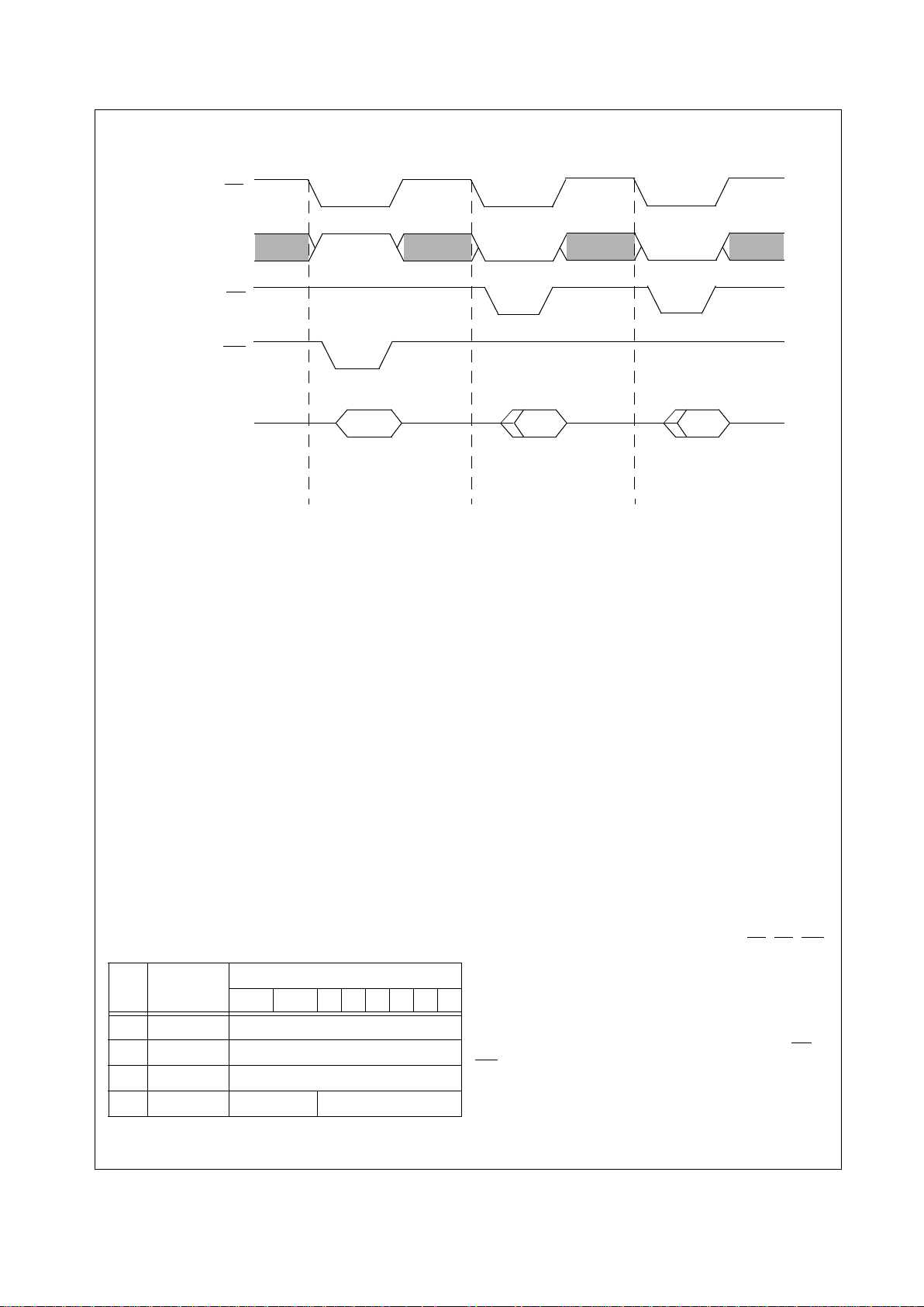
ALE
ALE
CS
AD[7:0]
DATA
RD or WR
ADDR
Figure7. Multiplexed Mode Basic Read/Write Timing
12 www.national.com
7.0 DMA Support
The USBN9602 supports DMA transfers with an external
DMA controller to and from Endpoints 1 through 6. In this
mode, the device pins DRQ and DACK
are used in addi-
tion to the parallel interface pins RD
or WR and the data
D[7:0] pins. The DMA mode can only be used with the
parallel interface modes (MODE1 tied to GND). The read
or write address is generated internally and the state of
the A0/ALE pin is ignored during a DMA cycle.
The DMA support logic has a lower priority than the parallel interface. CS
needs to stay inactive during a DMA cy-
cle. If CS
becomes active, DACK is ignored and a regular
read/write operation is performed. Only one Endpoint can
be enabled at a given time to issue a DMA request when
data is received or transmitted.
To enable DMA transfers, the following steps must be performed:
1. The local CPU programs the DMA controller for fly-by
demand mode transfers. In this mode, transfers occur
only when the USBN9602 requests them via the DRQ
pin. The data is read/written from/to the USBN9602 receive/transmit FIFO and written/read into/from local
memory during the same bus transaction.
2. The DMA address counter is programmed to point to the
destination memory block in the local shared memory,
and the byte count register is programmed with the number of bytes in the block to be transferred.
3. The DMA request enable bit and DMA source bits are set
in the USBN9602. In addition, the software must set the
respective Endpoint enable bit.
4. The USB host can now perform USB bulk or isochronous
data transfers over the USB bus to the receive FIFO or
from the transmit FIFO in the USBN9602.
5. If the FIFO’s warning limit is reached or the transmis-
sion/reception is completed, a DMA request/acknowledge sequence is started for the predetermined number
of bytes. The time at which a DMA request is issued depends on the selected DMA Mode (controlled by the
DMACNTRL.DMOD bit), the current status of the endpoint FIFO, and the FIFO warning enable bits. A DMA request can be issued immediately.
6. After the DMA controller is granted control of the bus, it
drives a valid memory address and asserts DACK
and
RD
or WR, thus transferring a byte from the USBN9602
receive FIFO to memory or from memory to the transmit
FIFO. This process continues until the DMA byte count,
within the DMA controller, reaches zero.
7. After the programmed amount of data is transferred, the
firmware needs to do one of the following (depending on
the transfer direction and mode): queue the new data for
transmission by setting the TXCx.TX_EN bit, set the
end-of-packet marker by setting the TXCx.TX_LAST bit,
re-enable reception by setting the RXCx.RX_EN bit, or
check whether the last byte of the packet was received
(RXSx.RX_LAST).
The DMA transfer can be halted at any time by resetting
the USBN9602 DMA request enable bit. If the USBN9602
DMA request enable bit is cleared during the middle of a
DMA cycle, the current cycle is completed before the
DMA request is terminated.
Figure 8 shows the basic DMA read timing and Figure 9
shows the basic DMA write timing.
DACK
DRQ
D[7:0]
WR
input
Figure8. DMA Write to USBN9602
DACK
DRQ
D[7:0]
RD
output
Figure9. DMA Read from USBN9602
13 www.national.com
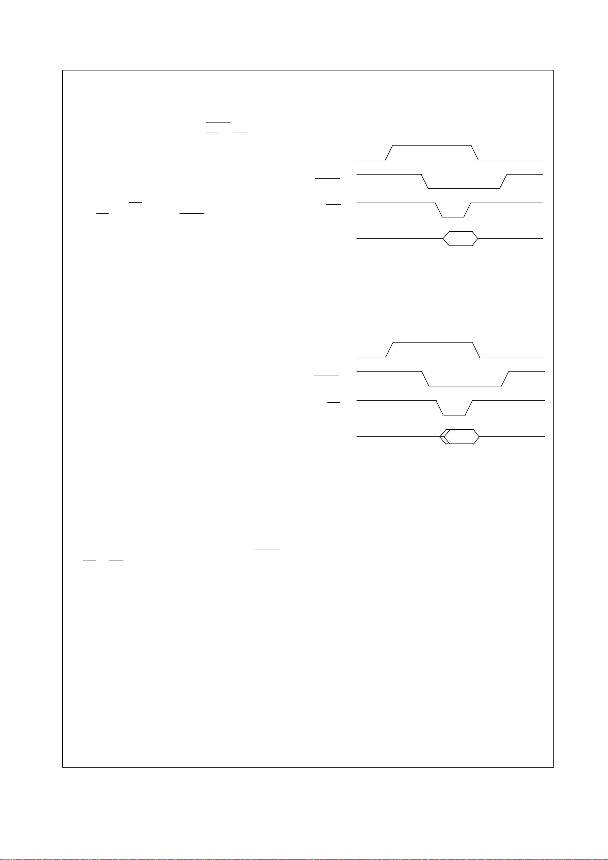
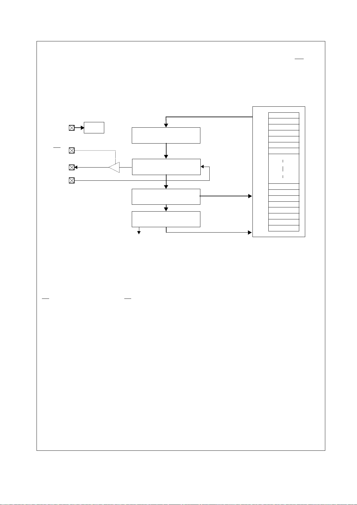
8.0 MICROWIRE/PLUS Interface
The MICROWIRE/PLUS interface allows the USBN9602
to function as a peripheral of a CPU or microcontroller via
a serial interface. This mode is selected by pulling the
MODE1 pin high and the MODE0 pin low. The MICROW-
IRE/PLUS mode uses pins called chip select (CS)
, serial
clock (SK), serial data in (SI), and serial data out (SO), as
shown in Figure 10.
The MICROWIRE interface is enabled by a falling edge of
CS
and reset with a rising edge of CS. Data on SI is shifted in after the rising edge of SK and data is shifted out on
SO after the falling edge of SK. Data transfer from and to
the shift register is done after the falling edge of the eighth
SK clock. Data is transferred with the most significant bit
first. Table1 summarizes the available commands for the
MICROWIRE interface.
Note: A write operation to any register always reads out the contents of the
register after the write occurs and shifts out that data in the next cycle. This
read does not clear the bit in the respective register, even for a clear-on-read
(“Cor”) type bit. An exception is writing to the TXDx (transmit data) registers,
which causes undefined data to be read out during the next cycle.
SO
SK
SI
0x00
0x3F
DATA_IN
CS
DATA OUT
DATA IN
REGISTER FILE
DATA_OUT
ADDR
ADDRESS
Figure10. MICROWIRE Interface Block Diagram
SHIFT REG
CMD[1:0]
SYNC
8.0 MICROWIRE/PLUS Interface (Continued)
14 www.national.com
Reading the data is done by shifting in the 2-bit command
(CMD) and the 5-bit address (RADDR or WADDR) while
simultaneously shifting out read data from the previous
address.
Writing data can be done in standard mode or burst
mode. The standard mode requires two bytes: the command and address being shifted in and the data being
shifted in. In burst mode, the command and address are
transferred first, and then consecutive data is written to
that address. The burst mode is terminated by CS
going
inactive (high).
For the MICROWIRE interface, Figure 11 shows the basic
read timing, Figure 12 shows the standard write timing,
and Figure 13 shows the write timing in burst mode.
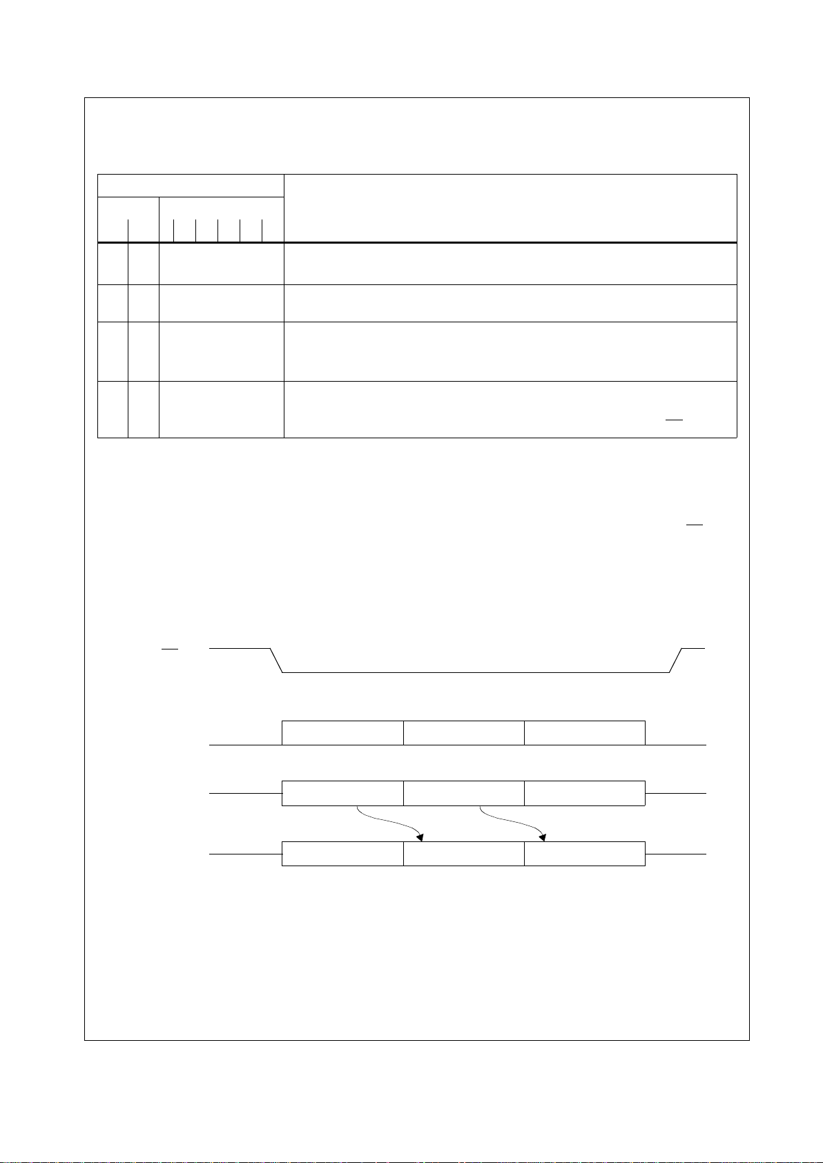
Table1. MICROWIRE Command/Address Byte Format
Byte Transferred
Sequence initiated. One cycle equals eight SK clocks. Data is transferred after the
eighth SK. clock of one cycle.
CMD ADDR
1 0 5 4 3 2 1 0
0 0
RADDR
(read)
Cycle 1:
Cycle 2:
Shift in CMD/RADDR; shift out previous read data
Shift in next CMD/ADDR; shift out RADDR data
0 1 x
Cycle 1:
No action; shift out previous read data (does not clear CoR bits)
1 0
WADDR
(normal write)
Cycle 1:
Cycle 2:
Shift in CMD/WADDR; shift out previous read data
Shift in WADDR write data; shift out WADDR read data (does
not clear CoR bits)
1 1
WADDR
(burst write)
Cycle 1:
Cycle 2-n:
Shift in CMD/WADDR; shift out previous read data
Shift in WADDR write data; shift out WADDR read data (does
not clear CoR bits); terminate this mode by pulling CS
high
CS
SK
SO
8 Cycles
SI
8 Cycles 8 Cycles
CMD = 0x ADDR CMD = 0x ADDR new command
undefined data Read Data Read Data
Figure11. MICROWIRE Interface Basic Read Timing
 Loading...