NATIONAL SEMICONDUCTOR TP5089N Datasheet

TP5089 DTMF (TOUCH-TONE) Generator
TP5089 DTMF(TOUCH-TONE) Generator
December 1991
General Description
The TP5089 is a low threshold voltage, field-implanted, metal gate CMOS integrated circuit. It interfaces directly to a
standard telephone keypad and generates all dual tone multi-frequency pairs required in tone-dialing systems. The tone
synthesizers are locked to an on-chip reference oscillator
using an inexpensive 3.579545 MHz crystal for high tone
accuracy. The crystal and an output load resistor are the
only external components required for tone generation. A
MUTE
OUT logic signal, which changes state when any key
is depressed, is also provided.
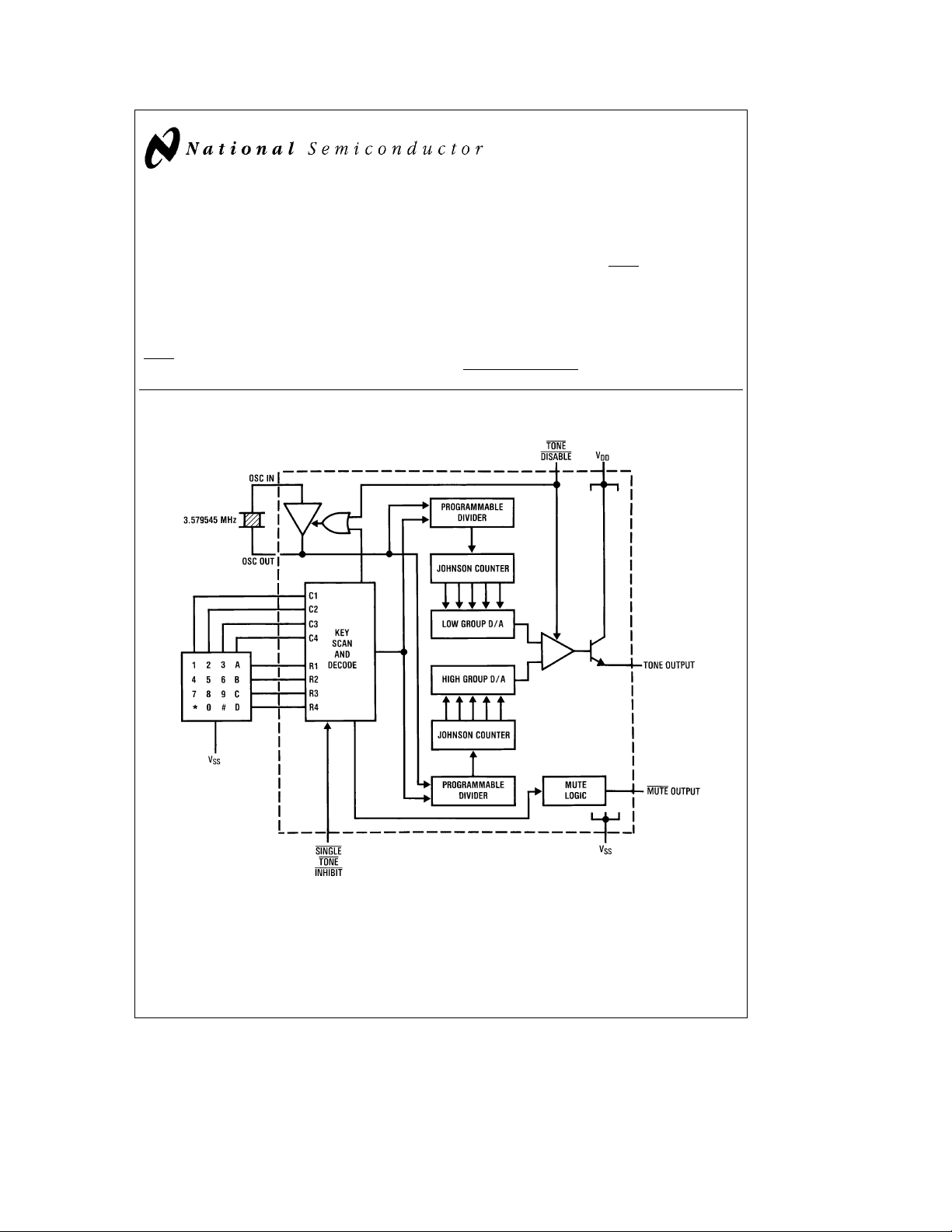
Block Diagram
Features
Y
3.5V–10V operation when generating tones
Y
2V operation of keyscan and MUTE logic
Y
Static sensing of key closures or logic inputs
Y
On-chip 3.579545 MHz crystal-controlled oscillator
Y
Output amplitudes proportional to supply voltage
Y
High group pre-emphasis
Y
Low harmonic distortion
Y
Open emitter-follower low-impedance output
Y
SINGLE TONE INHIBIT pin
FIGURE 1
TL/H/5057– 1
C
1995 National Semiconductor Corporation RRD-B30M115/Printed in U. S. A.
TL/H/5057

Absolute Maximum Ratings
If Military/Aerospace specified devices are required,
please contact the National Semiconductor Sales
Office/Distributors for availability and specifications.
Supply Voltage (V
Maximum Voltage at Any Pin V
Electrical Characteristics Unless otherwise noted, limits printed in BOLD characters are guaranteed for V
3.5V to 10V, T
correlation with other production tests and/or product design and characterization.
b
VSS) 15V
DD
e
0§Ctoa60§C by correlation with 100% electrical testing at T
A
DD
a
0.3V to V
b
0.3V
SS
Operating Temperature
Storage Temperature
Maximum Power Dissipation 500 mW
e
25§C. All other limits are assured by
A
Parameter Conditions Min Typ Max Units
Minimum Supply Voltage for Keysense
and MUTE
Logic Functions
Minimum Operating Voltage
for generating tones
Operating Current Mute open
Idle R
Generating Tones V
L
DD
e %
e
3.5V
2V
3.5 V
2 25 mA
1.1 2.5 mA
Input Resistors
COLUMN and ROW (Pull-Up) 25 50 kX
SINGLE TONE INHIBIT
TONE DISABLE
(Pull-Down) 120 kX
(Pull-Up)
Input Low Level 0.2 V
Input High Level 0.8 V
MUTE OUT Sink Current V
(COLUMN and ROW Active) V
MUTE Out Leakage Current V
Output Amplitude R
Low Group V
Output Amplitude R
High Group V
Mean Output DC Offset V
e
3.5V
DD
e
0.5V
o
e
V
o
DD
e
240 X
L
e
3.5V
DD
e
R
240X
L
e
10V
V
DD
e
240X
L
e
3.5V
DD
e
R
240X
L
e
10V
V
DD
e
3.5V 1.3 V
DD
e
V
10V 4.6 V
DD
DD
0.4 mA
1 mA
190 250 340 mVrms
510 700 880 mVrms
270 340 470 mVrms
735 955 1265 mVrms
High Group Pre-Emphasis 2.2 2.7 3.2 dB
Dual Tone/Total Harmonic Distortion Ratio V
e
DD
1 MHz Bandwidth
4V, R
e
240X
L
b
23
Start-Up Time (to 90% Amplitude) 3 5 mS
Note 1: RLis the external load resistor connected from TONE OUT to VSS.
Note 2: Crystal specification: Parallel resonant 3.579545 MHz, R
s
150 X,Le100 mH, C
S
e
e
5 pF, C
O
I
0.02 pF.
b
30§Ctoa60§C
b
55§Ctoa150§C
DD
b
22 dB
DD
e
V
V
2
 Loading...