NATIONAL SEMICONDUCTOR TP5088WM, TP5088N Datasheet

TP5088 DTMF Generator for Binary Data
TP5088 DTMF Generator for Binary Data
October 1991
General Description
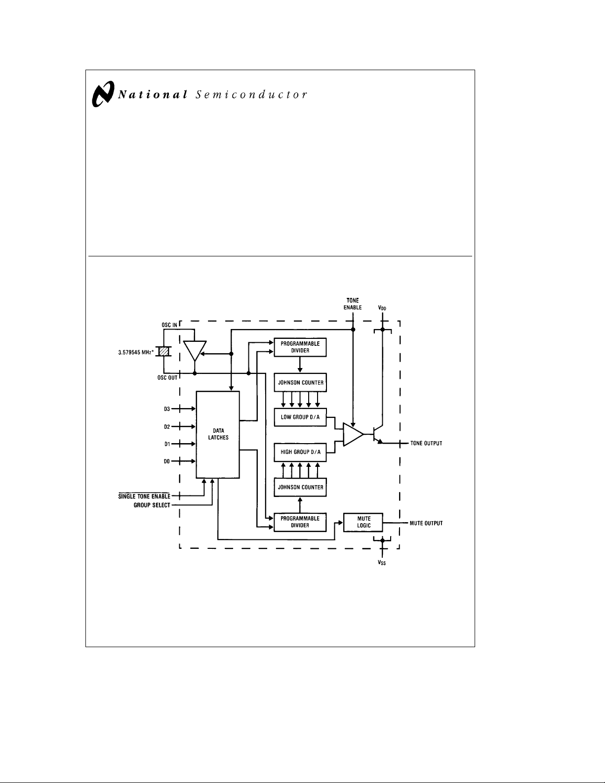
This CMOS device provides low cost tone-dialing capability
in microprocessor-controlled telephone applications. 4-bit
binary data is decoded directly, without the need for conversion to simulated keyboard inputs required by standard
DTMF generators. With the TONE ENABLE input low, the
oscillator is inhibited and the device is in a low power idle
mode. On the low-to-high transition of TONE ENABLE, data
is latched into the device and the selected tone pair from
the standard DTMF frequencies is generated. An open-drain
N-channel transistor provides a MUTE output during tone
generation.
Block Diagram
Features
Y
Direct microprocessor interface
Y
Binary data inputs with latches
Y
Generates 16 standard tone pairs
Y
On-chip 3.579545 MHz crystal-controlled oscillator
Y
Better than 0.64% frequency accuracy
Y
High group pre-emphasis
Y
Low harmonic distortion
Y
MUTE output interfaces to speech network
Y
Low power idle mode
Y
3.5V–8V operation
*Crystal Specification: Parallel Resonant 3.579545 MHz, R
C
1995 National Semiconductor Corporation RRD-B30M115/Printed in U. S. A.
TL/H/5004
s
150X,Le100 mH, C
S
e
0
5 pF, C
1
e
0.02 pF.
TL/H/5004– 1

Absolute Maximum Ratings
If Military/Aerospace specified devices are required,
please contact the National Semiconductor Sales
Office/Distributors for availability and specifications.
Supply Voltage (V
MUTE Voltage 12V
Maximum Voltage at
Any Other Pin V
b
VSS) 12V
DD
a
0.3V to V
DD
b
0.3V
SS
Operating Temperature, T
Storage Temperature
A
b
30§Ctoa70§C
b
55§Ctoa150§C
Maximum Power Dissipation 500 mW
Electrical Characteristics
Unless otherwise noted, limits printed in BOLD characters are guaranteed for V
correlation with 100% electrical testing at T
or product design and characterization.
e
25§C. All other limits are assured by correlation with other production tests and/
A
DD
e
3.5V to 8V, T
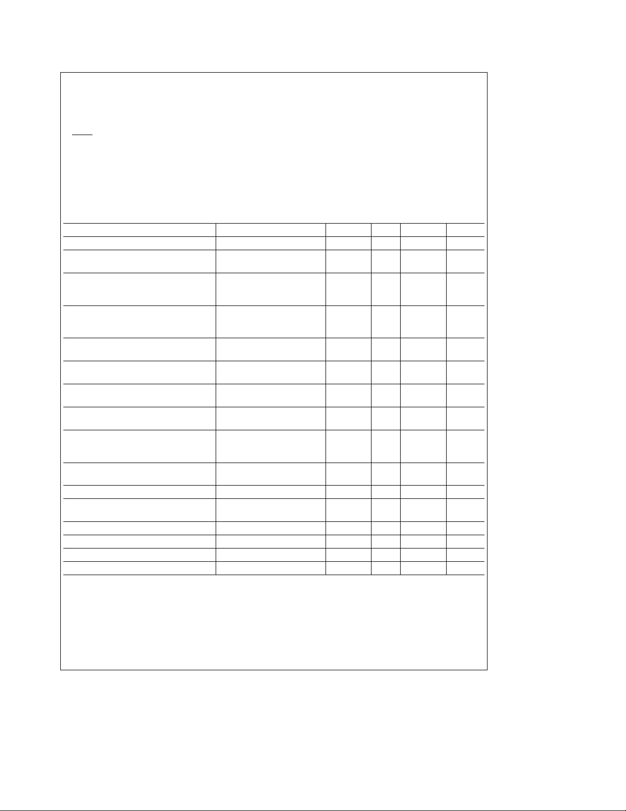
Parameter Conditions Min Typ Max Units
Minimum Supply Voltage, VDD(min) Generating Tones 3.5 V
Minimum Supply Voltage for Data Input,
TONE ENABLE and MUTE Logic Functions
2V
Operating Current
Idle R
Generating Tones V
e %
, D0–D3 Open 55 350 mA
L
e
3.5V, Mute Open 1.5 2.5 mA
DD
Input Pull-Up Resistance
D0–D3 100 kX
TONE ENABLE 50 kX
Input Low Level
TONE ENABLE, D0–D3 0.2 V
Input High Level
TONE ENABLE, D0–D3 0.8 V
MUTE OUT Sink Current V
(TONE ENABLE LOW) V
MUTE OUT Leakage Current V
(TONE ENABLE HIGH) V
Output Amplitudes R
Low Group V
High Group T
Mean Output DC Offset V
e
3.5V
DD
e
0.5V
o
e
3.5V
DD
e
V
o
DD
e
240 X
L
e
3.5V
DD
e
25§C
A
e
3.5V 1.2 V
DD
e
V
8V 3.6 V
DD
DD
0.4 mA
130 170 220 mVrms
180 230 310 mVrms
High Group Pre-Emphasis 2.2 2.7 3.2 dB
Dual Tone/Total Harmonic Distortion Ratio 1 MHz Bandwidth, V
e
R
240X
L
Start-Up Time (to 90% Amplitude), t
Data Set-Up Time, tS(
Data Hold Time, t
Data Duration t
Note 1: RLis the external load resistor connected from TONE OUT to VSS.
Figure 2
H
W
OSC
)V
e
5V 100 ns
DD
e
V
5V 280 ns
DD
e
V
5V 600 ns
DD
DD
e
5V
b
20 dB
e
0§Ctoa70§Cby
A
DD
1 mA
4ms
V
V
2
 Loading...