NATIONAL SEMICONDUCTOR TP3420AV309, TP3420AV308, TP3420AN308 Datasheet

TP3420A
ISDN S/T Interface Device
General Description
The TP3420A is an enhanced version of the TP3420, with a
number of upgraded features for compliance with the new
release of ANSI T1.605-1991 and CCITT I-430. At initial
power-up the device is fully backwards compatible with the
TP3420 device, and modifications to the firmware are only
required to take advantage of the new features.
The TP3420A S Interface Device (SID™) is a complete
monolithic transceiver for data transmission on twisted pair
subscriber loops. It is built on National’s advanced 1.0 micron double-metal CMOS process, and requires only a
single +5V supply. All functions specified in CCITT recommendation I.430 (1991) and ANSI T1.605 (1991) for ISDN
basic access at the “S” and “T” interfaces are provided, and
the device can be configured to operate either in a TE (Terminal Equipment), inan NT-1 or NT-2 (Network Termination)
or as a PABX line-card or trunk-card device.
As specified in I.430, full-duplex transmission at 192 kb/s is
provided on separate transmit and receive twisted wire pairs
using inverted Alternate Mark Inversion (AMI) line coding. 2
“B” channels, each of 64 kb/s, and 1 “D” channel at 16 kb/s
are available for users’ data. In addition, the TP3420A provides the 800 b/s “S1”, “S2” & “Q” multiframe channels for
Layer 1 maintenance.
All I.430 wiring configurations are supported by the TP3420A
SID, including the “passive bus” for up to 8 TE’s distributed
within 200 meters of low capacitance cable, and
point-to-point and point-to-star connections up to at least
1500 meters (24AWG). Adaptive receive signal processing
ensures low bit error rates on any of the standard types of
cable pairs commonly found in premise wiring installations
when tested with the noise sources specified in I.430.
Features
n 2B+D4-wire 192 kb/s transceiver
n Selectable TE or NT mode
n Exceeds I.430 range: 1.5 km point-to-point
n Adaptive receiver for high noise immunity
n Adaptive and fixed timing options for NT-1
n Clock resynchronizer and elastic buffers for NT-2/LT
n Slave-slave mode for NT-2 trunks
n Extensive hardware support for SC1, SC2 and Q
channel messaging
n Bipolar violation detection and FECV messaging
n Selectable system interface formats
n MICROWIRE
™
and SCP compatible serial control
interface
n TP3054/7 Codec/Filter COMBO
™
compatibility
n Single +5V supply
n 20-pin package DIP, PLCC
Applications
n Same Device for NT, TE and PBX Line Card
n Point-to-Point Range Extended to 1.5 km
n Point-to-Multipoint for all I.430 Configurations
n Easy Interface to:
LAPD Processor MC68302, HPC16400
Terminal Adapter MC68302, HPC16400
Codec/Filter COMBO TP3054/7 and TP3076
“U” Interface Device TP3410
Line Card Backplanes — No External PLL Needed
n Line Monitor Mode for Test Equipment
TRI-STATE®is a registered trademark of National Semiconductor Corporation.
COMBO
™
, MICROWIRE™and SID™are trademarks of National Semiconductor Corporation.
PRELIMINARY
July 1994
TP3420A ISDN S/T Interface Device
© 1999 National Semiconductor Corporation DS009143 www.national.com
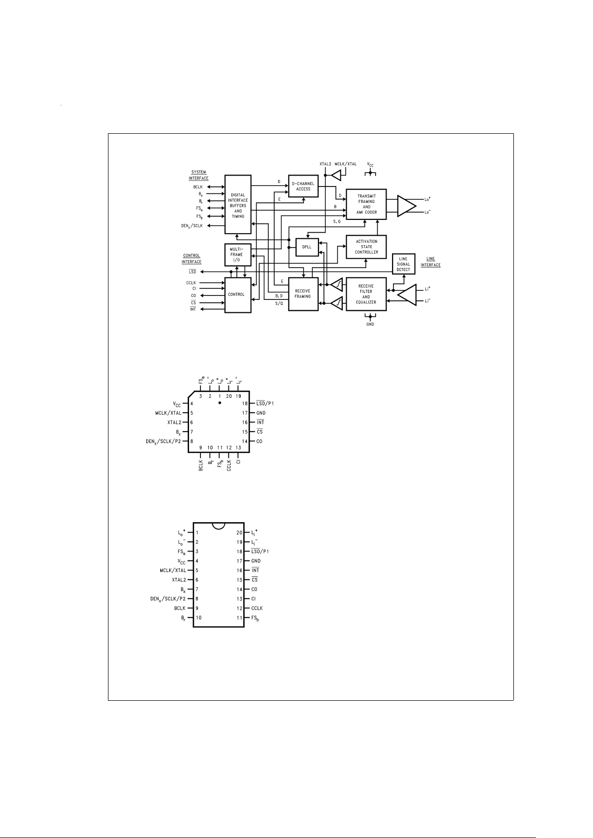
Block Diagram
Connection Diagrams
Pin Descriptions
Name Description
GND Negative power supply pin, normally 0V
(ground). All analog and digital signals
are referenced to this pin.
V
CC
Positive power supply input, which must
be +5V
±
5%relative to GND.
MCLK/XTAL The 15.36 MHz Master Clock input, which
requires either a crystal (Note 1) to be
tied between this pin and XTAL2, or a
CMOS logic level clock input from a
stable source. When using a crystal, a
total of 33 pF load capacitance to GND
must also be connected. (Note 2)
XTAL2 The output of the crystal oscillator, which
should be connected to one end of the
crystal, and 33 pF of load capacitance to
GND. (Note 2) If using an external master
Clock via the MCLK pin, leave the XTAL2
pin unconnected.
BCLK The Bit Clock pin, which determines the
data shift rate for “B” and “D” channel
data at the digital interface. When NT
mode or TES mode is selected, BCLK is
a TTL/CMOS input which may be any
multiple of 8 kHz from 256 kHz to 4.096
MHz. It need not be synchronous with
MCLK.
When TEM mode is selected, this pin is a
CMOS output at frequency selected by
the Digital Interface Format. This clock is
phase-locked to the received line signal
and is synchronous with the data on B
x
and Br.
DS009143-1
TP3420A SID
DS009143-20
Order Number TP3420AV
See NS Package Number V20A
TP3420A SID
DS009143-2
Top View
Order Number TP3420AJ or TP3420AN
See NS Package Number J20A or N20A
www.national.com 2

Pin Descriptions (Continued)
Name Description
FS
a
In NT modes and TES mode, this pin is
the Transmit Frame Sync pulse
TTL/CMOS input, requiring a positive
edge to indicate the start of the active
channel time for transmit “B” and “D”
channel data into B
x
. In TEM mode only,
this pin is a digital output pulse whose
positive indicates the start of the “B”
channel data transfer at both B
x
and Br.
FS
b
(Pin 11)
In NT modes and TES mode, this pin is
the Receive Frame Sync pulse
TTL/CMOS input, requiring a positive
edge to indicate the start of the active
channel time of the device for receive “B”
and “D” channel data out from B
r
.InTEM
mode only, when digital interface Format
1 is selected, this pin is an 8-bit wide
pulse which indicates the active slot for
the B2 channel on the digital interface.
The DCKE command will alter the
function of this pin. See
Table 2
for
details.
B
x
TTL/CMOS input for “B” and “D” channel
data to be transmitted to the line; must be
synchronous with BCLK.
B
r
CMOS output for “B” and “D” channel
data received from the line, which is
synchronous with BCLK. When not
shifting data, this pin is TRI-STATE
®
.
DEN
x
/p2
(Pin 8)
In TEM mode, this pin by default is a
CMOS output which is normally low and
pulses high to indicate the active bit-times
for “D” channel Transmit data at the B
x
input. It is intended to be gated with
BCLK to control the shifting of data from
layer 2 device to the TP3420A transmit
buffer.
In NT modes, this pin by default is a
pulse output (DEN
x
) which occurs in
every 8 KHz frame and indicates the
location of D channel data input on the B
x
pin.
In TES mode, this pin by default is an
output synchronized clock (SCLK) at the
frequency selected by the Digital
Interface Format. This clock is
phase-locked to the received line signal,
and is intended to be used as the BCLK
source.
This pin called P2 in
Table 1
can also be
programmed to provide alternate
functions. See
Table 1
for details.
CI MICROWIRE control channel serial data
TTL/CMOS input.
Name Description
CO Control channel serial data CMOS output
for status information. When not enabled
by CS, this output is TRI-STATE.
CCLK TTL/CMOS clock input for the Control
Channel.
CS
Chip Select input which enables the
control channel data to be shifted in and
out when pulled low. When high, this pin
inhibits the Control interface.
INT
Interrupt output, a latched n-channel
open-drain output signal which is
normally high impedance, and goes low
to indicate a change of status of the loop
transmission system.
LSD/P1
(Pin 18)
In all modes, this pin by default is the
Line Signal Detect output, an n-channel
open-drain output which is normally
high-impedance, but pulls low when the
device is powered down and a received
line signal is detected. It is intended to be
used to “wake-up” a microprocessor from
a low-power idle mode. This output is
high impedance when the device is
powered up.
This pin P1 in
Table 1
can also be
programmed to provide alternate
functions. See
Table 1
for details.
L
o
+, Lo− Transmit AMI signal differential outputs to
the line transformer. When used with a
2:1 step-down transformer, the line signal
conforms to the output pulse masks in
I.430.
L
i
+, Li− Receive AMI signal differential inputs
from the line transformer. The L
i
− pin is
also the internal voltage reference pin,
and must be decoupled to GND with a 10
µf capacitor in parallel with a 0.1 µF
ceramic capacitor.
Note 1: Crystal specification: 15.36 MHz parallel resonant; Rs≤ 150Ω,
C
L
=
20 pF and C
O
<
7pF.
Note 2: The 33 pF includes any board capacitance.
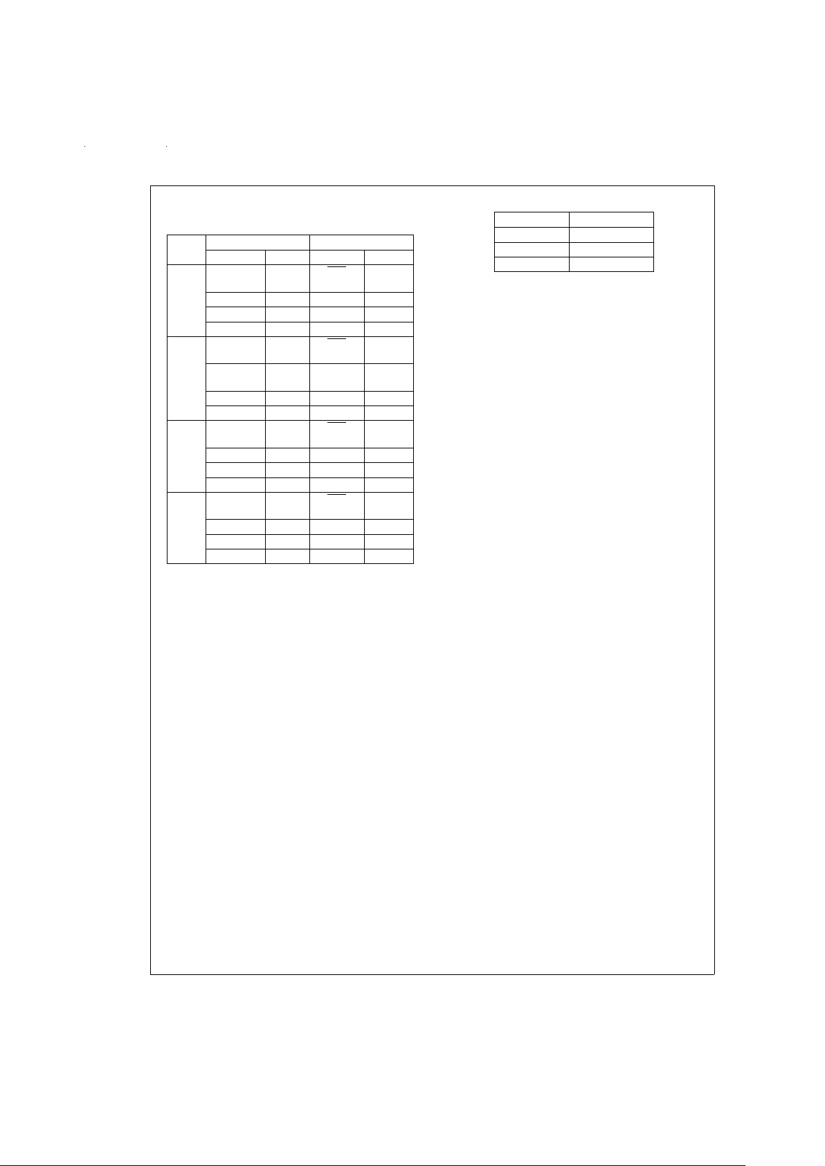
ALTERNATE PIN FUNCTIONS
With a MICROWIRE command PINDEF (B'1110 0 x2 x1 x0)
the pin signal functions of these pins can be changed to provide alternate functions (see
Table 1
and the MICROWIRE
command in
Table4
). “*” indicates the default pin function after a device mode selection. Power-up default device mode
is NTA.
www.national.com3
Pin Descriptions (Continued)
TABLE 1. Alternate Pin Function Assignment
Device
Mode
P2 - Pin 8 P1 - Pin 18
Function x
2
Function x1,x
0
TEM DENx
(Note 3)0(Note 3)
LSD 00
(Note 3)
SCLK 1 DENr 01
SCLK 10
DENx 11
TES DENx 0 LSD
00
(Note 3)
SCLK
(Note 3)1(Note 3)
DENr 01
SCLK 10
DENx 11
NTA DENx
(Note 3)0(Note 3)
LSD
00
(Note 3)
NTF SCLK 1 DENr 01
SCLK 10
DENx 11
MMA DENx
(Note 3)0(Note 3)
LSD
00
(Note 3)
SCLK 1 DENr 01
SCLK 10
DENx 11
PINDEF command is coded as X’EX (i.e. 11100x2x1x0).
Note 3: Default pin function after device mode selection.
SIGNAL DESCRIPTION
SCLK is an output synchronized clock at the frequency selected by the Digital Interface Format. This clock is
phase-locked to the received line signal, and is intended to
be used as the BCLK source.
LSD is the Line Signal Output, an n-channel open-drain output that is normally high-impedance, but pulls low when the
device is powered down and a received line signal is detected. It is intended to be used to “wake-up” a microprocessor from a low-power idle mode. This output is a high impedance when the device is powered up.
DENr is a CMOS output that is normally low and pulses high
to indicate the active bit times for “D” channel Receive data
at the B
r
output pin. It is intended to be gated with BCLK to
control the shifting of data from the TP3420A receive buffer
to a layer 2 device.
DENx is a CMOS output that is normally low and pulses high
to indicate the active bit times for D channel Transmit data at
the B
x
input. It is intended to be gated with BCLK to control
the shifting of data from a layer 2 device to the TP3420A’s
transmit buffer. In NT mode, this pulse occurs every 8 kHz
frame and indicates the location of D channel data input on
the B
x
pin.
ADDITIONAL PIN CONFIGURATION
The TP3420A in TEM mode can be configured to interface
with the Motorola layer-2 devices such as the MC68302 and
the MC145488. A PINDEF (X’E1) command followed by a
DCKE (X’F1) command will alter the TP3420A pin functions
as shown in
Table2
. Other configurations of PINDEF are not
supported.
TABLE 2.
Pin Number Pin Function
8 DTCK
11 TxD
18 DRCK
Where:
•
DCLK is a burst clock output intended to be used as a
clock source for the transmitter of an HDLC device.
•
TxD is an input being sampled on the rising edge of
DCLK during the active D-channel timeslot.
•
DRCK is a burst clock output which pulses 2 BCLK periods every 8 kHz frame. This output is intended to be used
as a clock source for the receiver of an HDLC device. The
D-channel data at B
r
is transmitted on the falling edge of
the DRCK.
Functional Description
DEVICE MODES
The TP3420A can be programmed into one of four possible
modes. For NT applications select NT Adaptive timing (NTA)
for all wiring configurations except a Short Passive Bus, for
which NT Fixed Timing (NTF) should be selected. In TE applications, select TE Master mode (TEM) for the device to be
the master (source) of clocks at the digital interface, or select
TE Slave mode (TES) for the digital interface to accept
clocks from the system.
Selection of these modes is described in the section on Control Register instructions.
POWER-ON DEVICE CONDITIONS
Following the initial application of power, the TP3420A SID
enters the power-down (de-activated) state, in which all the
internal circuits including the Master oscillator are inactive
and in a low power state except for the Line-Signal Detect
circuit; the line outputs L
o
+/Lo− are in a high impedance
state and the Digital System Interface is inactive. All bits in
the Control Register power-up as indicated in
Table 1
.In
both NT and TE modes, a Line-Signal Detect circuit monitors
the line while the device is powered-down, to enable loop
transmission to be initiated from either end.
POWER-OFF DEVICE CONDITION
When power to the TP3420A is turned off, the Line outputs
L
o
+/Lo− go into high impedance state, hence if a TE on a
passive bus lost power its transmit impedance still meets the
specification without any external relay (see AN665 for external protection components). The receiver impedance also
remains in specification.
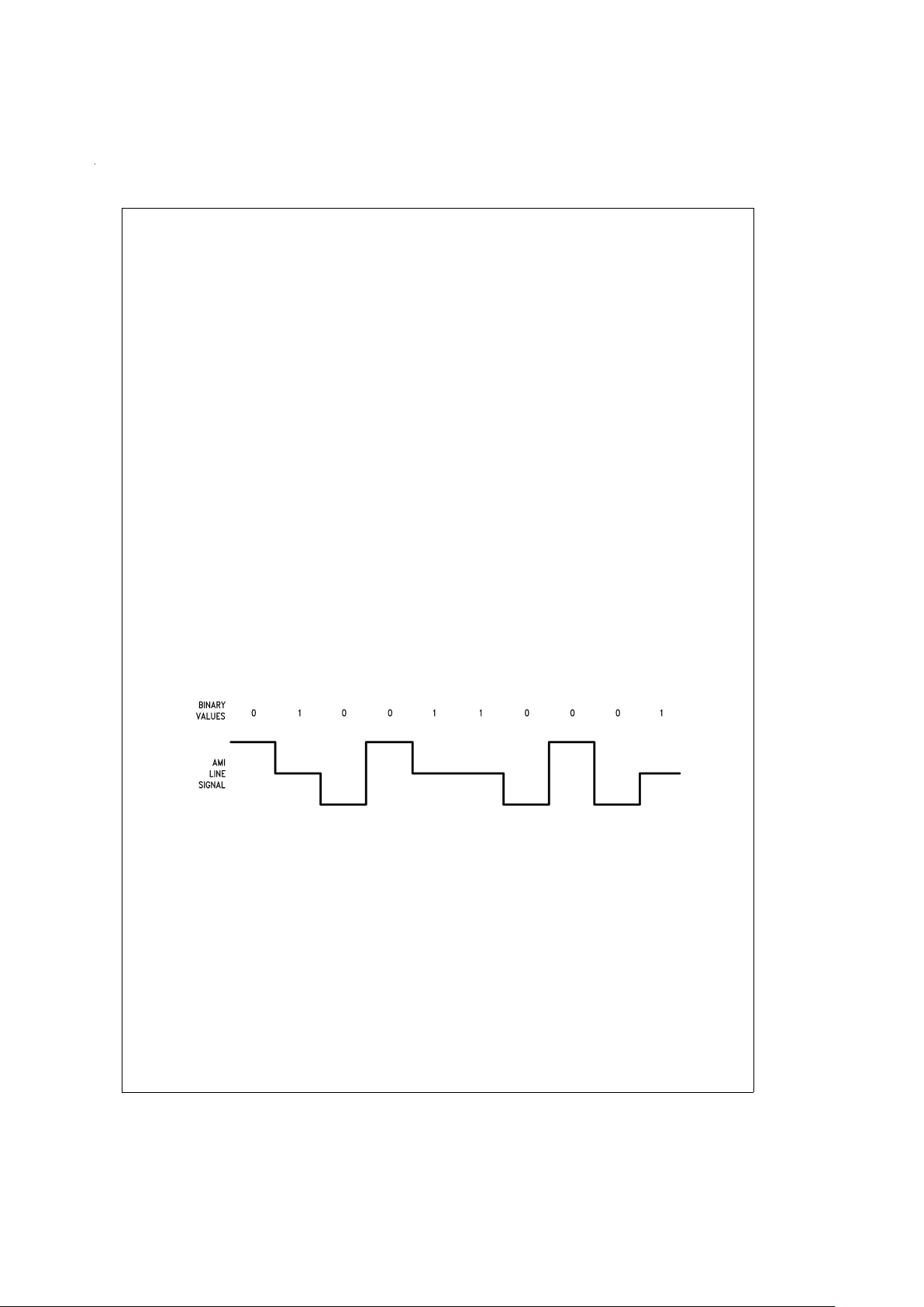
LINE CODING AND FRAME FORMAT
For both directions of transmission, Alternate-Mark Inversion
(AMI) coding with inverted binary is used, as illustrated in
Figure 1
. This coding rule requires that a binary ONE is represented by 0V high impedance output, whereas a binary
ZERO is represented by a positive or negative-going 100
%
duty-cycle pulse. Normally, binary ZEROs alternate in polarity to maintain a d.c.-balanced line signal.
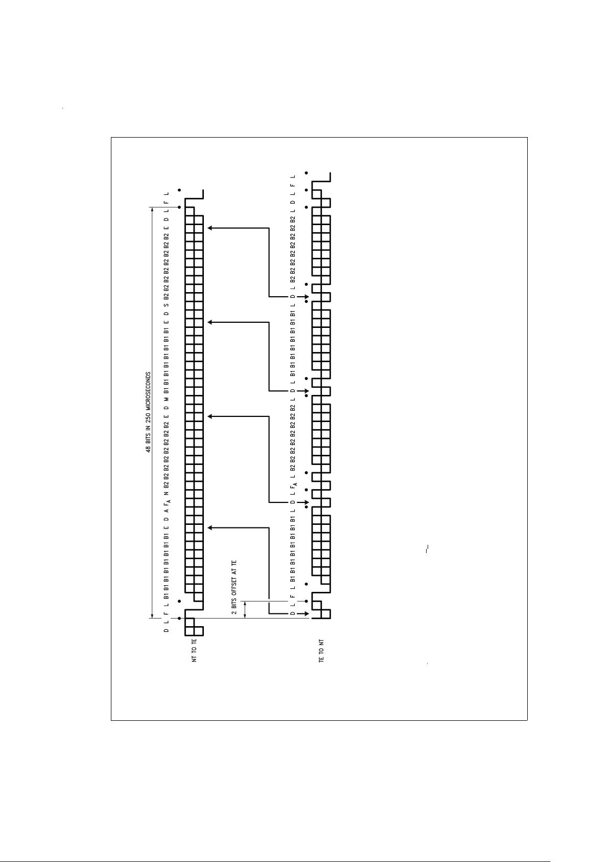
The frame format used in the TP3420A SID follows the
CCITT recommendation specified in I.430 and illustrated in
Figure 2
. Each complete frame consists of 48 bits, with a line
bit rate of 192 kb/s, giving a frame repetition rate of 4 kHz. A
violation of the AMI coding rule is used to indicate a frame
www.national.com 4
Functional Description (Continued)
boundary,by using a 0
+
bit followed by a 0−balance bit to indicate the start of a frame, and forcing the first binary zero
following the balance bit to be of the same polarity as the balance bit.
In the Network Termination (NT) to the Terminal Equipment
(TE) transmission direction the frame contains an echo
channel, the E bit, which is used to retransmit the D bits that
are received from the TE. The last bit of this frame is used as
a frame balancing bit. In the TE to NT direction,
d.c.-balancing is carried out for each channel, as illustrated
in
Figure 2
.
LINE TRANSMIT SECTION
The differential line-driver outputs, L
o
+ and Lo−, are designed to drive a transformer with an external termination resistor. A suitable 2:1 transformer, terminated in 50Ω, results
in a signal amplitude of nominally 750 mV pk on the line
which fully complies with the I.430 pulse mask specifications. When driving a binary 1 symbol the output presents a
high impedance in accordance with I.430. When driving a 0+
or 0− symbol a voltage-limited current source is turned on.
Short-circuit protection is included in the output stage;
over-voltage protection is required externally, see the Applications section.
LINE RECEIVE SECTION
The receive input signal should be derived via a 1:1 transformer, or a 1:2 transformer of the same type used for the
transmit direction. At the front-end of the receive section is a
continuous filter which limits the noise bandwidth. Tocorrect
pulse attenuation and distortion caused by the transmission
line in point-to-point and extended passive bus applications,
an adaptive equalizer enhances the received pulse shape,
thereby restoring a “flat” channel response with maximum
eye opening over a wide spread of cable attenuation characteristics. This equalizer is always enabled when either TE
mode or NT Mode Adaptive Sampling is selected, but is disabled for short passive bus applications when NT Mode
Fixed Sampling is selected. An adaptive threshold circuit
maximizes the Signal-to-Noise ratio in the eye at the detector for all loop conditions.
In NTF mode the receive baud sampling point is fixed relative to the transmit baud clock. This ensures accurate sampling of received pulses with differential delays on a passive
bus, thus extending the short passive bus range to over
250m of low capacitive cable.
In NTA and TE modes, the receive baud sampling is adaptive. In these modes, a DPLL (Digital Phase-Locked Loop)
recovers a low-jitter clock for optimum sampling of the received symbols. The MCLK input provides the reference
clock for the DPLL at 15.36 MHz. Clocks for the digital interface timing may either be derived from this recovered clock,
as in TE mode Digital System Interface Master, or may be
slaved to an external source, as in the T-interface side of an
NT-2 (TES mode). In TES and NT modes, re-timing circuitry
on the TP3420A allows the MCLK frequency to be plesiochronous (i.e., free-running) with respect to the network
clock, i.e. the 8 kHz FS
a
input. With a tolerance on the MCLK
oscillator of 15.36 MHz
±
100 ppm, the lock-in range of the
DPLL allows the network clock frequency to deviate up to
±
50 ppm from nominal.
When the device is powered-down (either on initial
powering-on of the device or after using a PDN command), a
Line-Signal Detect circuit is enabled to detect the presence
of incoming data if the far-end starts to activate the loop. The
LSD circuit is disabled by a Power-Up (PUP) command.
DS009143-4
FIGURE 1. Inverted AMI Line-Coding Rule
www.national.com5
Functional Description (Continued)
DS009143-5
Legend:
F
=
Framing bit
L
=
DC Balancing bit
D
=
D-channel bit
E
=
D-echo-channel bit
F
A
=
Auxiliary framing bit or Q Channel bit
M
=
Multiframe Sync bit
N
=
bit set to a binary value N
=
F
A
B1
=
bit within B-channel 1
B2
=
bit within B-channel 2
A
=
bit used for activation
S
=
S Channel bit
Note 4: Dots mark the boundaries of those parts of the frame that are independently DC-balanced
FIGURE 2. Frame Format
www.national.com 6

Functional Description (Continued)
DIGITAL SYSTEM INTERFACE
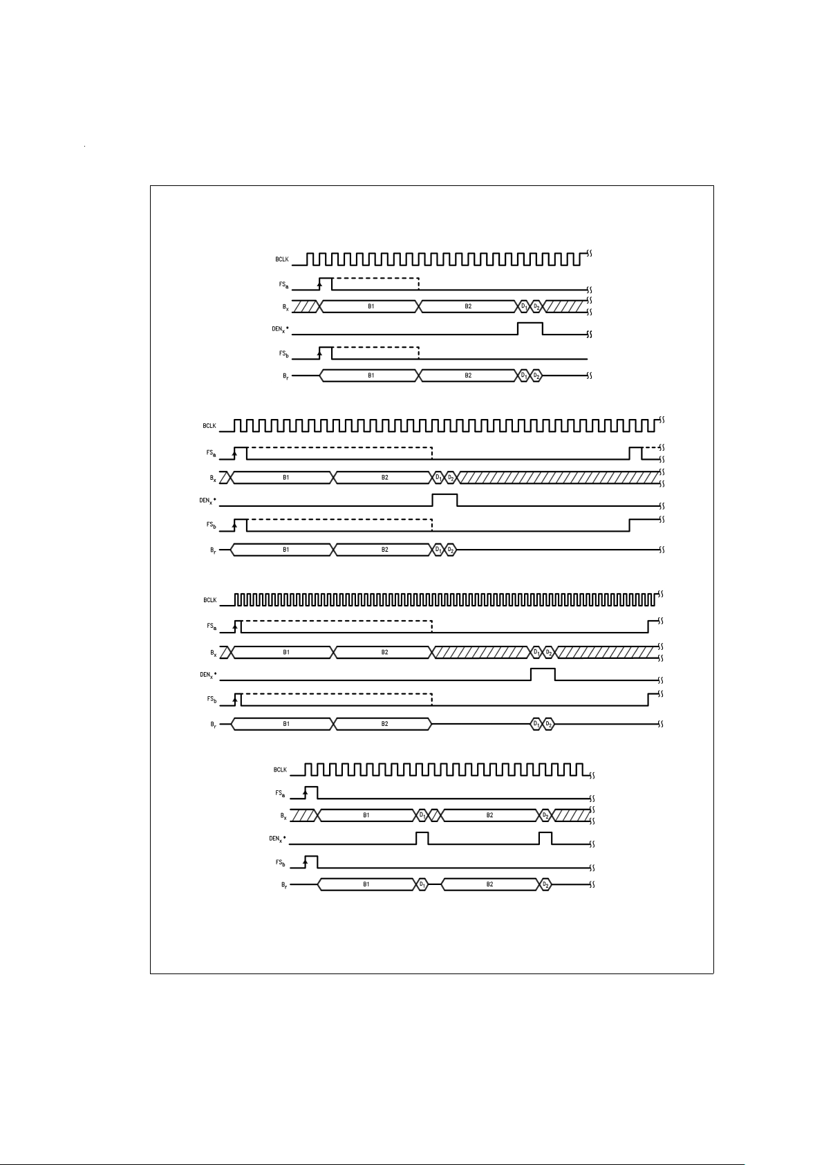
The Digital System Interface (DSI) on the TP3420A combines “B” and “D” channel data onto common pins to provide
maximum flexibility with minimum pin count. Several multiplexed formats of the B and D channel data are available as
shown in
Figure 3
. Selection is made via the Control Regis-
ter.
NTA,NTF and TES modes: at this interface, phase skew be-
tween transmit and receive frames may be accommodated
when the device is a slave at the Digital Interface (NT and
TES Modes) since separate frame sync inputs (
Figure 3
),
FS
a
and FSb, are provided. Each of these synchronizes a
counter which gates the transfer of B1 and B2 channels in
consecutive time-slots across the digital interface. The serial
shift rate is determined by the BCLK input, and may be any
multiple of 8 kHz from 256 kHz to 4.096 MHz. Thus, for applications on a PABX line-card (in NT mode), the “B” and “D”
channel slots can be interfaced to a TDM bus and assigned
to a time-slot.
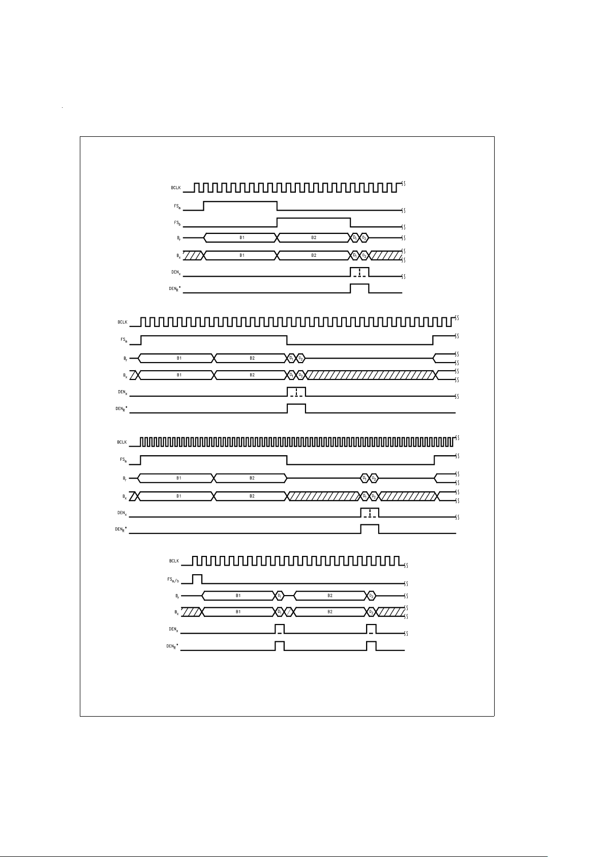
TEM mode: in TE Master Mode (TEM), FS
a
is an output (
Fig-
ure 4
) indicating the start of both transmit and receive “B”
channel data transfers. BCLK is also an output at the serial
data shift rate, which is dependent on the format selected,
see
Table 5
.
TES mode: for applications such as the network side of an
NT-2, e.g. a PBX trunk card, the TE Slave (TES) Mode is
provided. This “slave-slave” mode allows the transmission
side of the device to be a slave to the received frame timing,
while the Digital System Interface is also in a slave mode i.e.
FS
a
,FSband BCLK are inputs. The Digital System Interface
includes elastic buffers which allow any arbitrary phase relationship between each FS input and the received I.430
frame.
JITTER ABSORPTION AND PHASE WANDER BUFFERS
The TP3420A has an improved serial data buffer circuit to
handle larger amounts of phase wander exceeding the
specification of 18 µs pk-to-pk, regardless of the phase difference between the transmit and receive frames. A SLIP indicator interrupt is generated to inform the CPU if the phase
deviation between two clocks exceeds the boundary of the
circuit, causing the data buffers to adjust the internal delay to
accommodate this. Under some, but not all, circumstances
this will result in data errors as the slip occurs. Separate interrupt status values (SLIP— TX and SLIP — RX) indicate
the clock slippage in the transmit buffer or the receiver buffer.
TES Mode also provides a synchronized clock output
(SCLK) which is phase-locked to the received line signal;
SCLK may be used as the BCLK source.
TABLE 3. DSI Format Rates
BLCK as BCLK as
Format DSI Master DSI Slave
(Output) (Note 5) (Input)
1 2.048 MHz 256 kHz–4.096 MHz
2 256 kHz 256 kHz–4.096 MHz
BLCK as BCLK as
Format DSI Master DSI Slave
(Output) (Note 5) (Input)
3 512 kHz 512 kHz–4.096 MHz
4 2.56 MHz 256 kHz–4.096 MHz
Note 5: also SCLK output in TES Mode.
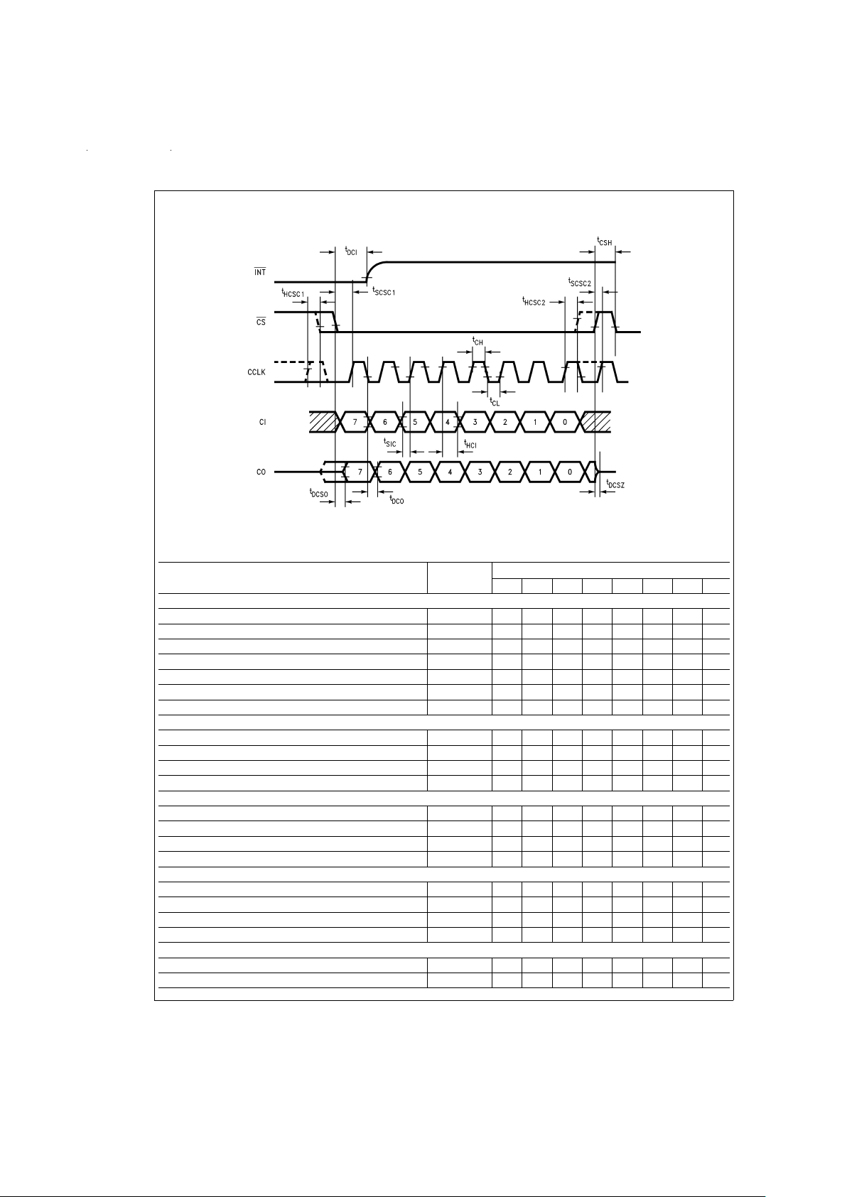
MICROWIRE CONTROL INTERFACE
A serial interface, which can be clocked independently from
the “B” and “D” channel system interface, is provided for microprocessor control of various functions in the TP3420. This
port can be used when the device is powered up or powered
down. All data transfers consist of a single byte shifted into
the Control Register via the CI pin, simultaneous with a
single byte shifted out from the Status Register via the CO
pin.
Data shifts in to CI on rising edges of CCLK and out from CO
on falling edges when CS is pulled low for 8 cycles of CCLK.
An Interrupt output, INT goes low to alert the microprocessor
whenever a change occurs in one or more of the conditions
indicated in the Status Register. This latched output is
cleared to a high impedance state by the first rising CCLK
edge after CS goes low. Interrupt Source(s) occurring while
another is still pending are stored in a stack and read in sequence, by causing another interrupt at the end of the current CS cycle (INT can go low only when CS is high). When
reading the Status Register the CI input is also enabled,
therefore a “dummy” command e.g. NOP(X’FF) must be
loaded into CI as CO is read.
Each source of an Interrupt event (
e.g.,
EI, AI, SLIP) in the
device has an internal latch, such that the occurrence of that
event is stored until read from the status register. Multiple
events will be reported in turn by the device in a circular
manner. There is no priority criteria. If multiple occurrences
of the same event occur (
e.g.,
EI, followed by AI and then EI)
and if left unserviced, than the second occurrence (of EI in
this example) will over-write the first. Also if a multiframe interrupt such as MFR1 interrupt is not serviced before a second occurrence of the MFR1 interrupt, then the second value
in the M1–M4 bits will overwrite the first. The DI interrupt
clears all pending interrupts and indicating the reset state of
the device. The LSD interrupt is generated independently
and is only valid while the device is in low power mode
(PDN). A PUP command resets the line signal detect circuit
and the LSD interrupt. A PDN command resets and
re-enables the LSD circuit and interrupt.
Figure 5
shows the timing for this interface, and
Table4
and
Table 5
list the control functions and status indicators.
FLEXIBLE MICROWIRE PORT
The MICROWIRE port of the TP3420A has been enhanced
such that it can connect to standard MICROWIRE master
devices (such as National’s microcontrollers of the HPC and
COP families) as well as the SCP interface master from the
Motorola microcontroller family. SCP is the Serial Control
Port on devices such as the MC68302 or the MC145488
HDLC. See the MICROWIRE port timing diagram and the
applications section.
www.national.com7
Functional Description (Continued)
Format 1
DS009143-10
Format 2
DS009143-13
Format 3
DS009143-11
Format 4
DS009143-12
*
Note: In TES mode, DENx outputs SCLK synchronized to the S interface. Format 1, SCLK=2.048 MHz, Format 2, SCLK=256 kHz, Format 3,
SCLK=512 kHz, Format 4, SCLK=2.56 MHz.
FIGURE 3. Digital System Interface Formats in NT and TES*modes (DSI Slave)
www.national.com 8
Functional Description (Continued)
Format 1
DS009143-14
Format 2
DS009143-15
Format 3
DS009143-16
Format 4
DS009143-17
*
Note: DENR signal is available on pin 18 after using the PINDEF command (see
Table 1
).
FIGURE 4. Digital System Interface Formats in TEM mode (DSI Master)
www.national.com9
Functional Description (Continued)
TABLE 4. Control Register Functions
Function Mnemonic Bit Number
76543210
Activation/Deactivation
No Operation NOP 11111111
Power-Down (Note 6) PDN 00000000
Power-Up PUP 00100000
Deactivation Request DR 00000001
Force INFO2 (NT only) FI2 00000010
Monitor Mode Activation MMA 00011111
Activation Request AR 00000011
Device Modes
NT Mode, Adaptive Sampling (Note 6) NTA 00000100
NT Mode, Fixed Sampling NTF 00000101
TE Mode, Digital System Interface Slave (Note 7) TES 00000110
TE Mode, Digital System Interface Master TEM 00000111
Digital Interface Formats
Digital System Interface Format 1 (Note 6) DIF1 00001000
Digital System Interface Format 2 DIF2 00001001
Digital System Interface Format 3 DIF3 00001010
Digital System Interface Format 4 DIF4 00001011
BCLK Frequency Settings
Set BCLK to 2.048 MHz BCLK1 10011000
Set BCLK to 256 kHz BCLK2 10011001
Set BCLK to 512 kHz BCLK3 10011010
Set BCLK to 2.56 MHz BCLK4 10011011
B Channel Exchange
B Channels Mapped Direct, B1 to B1, B2 to B2 (Note 6) BDIR 00001100
B Channels Exchanged, B1 to B2, B2 to B1 BEX 00001101
DS009143-21
FIGURE 5. TP3240A Enhanced MICROWIRE Control Interface Timing
www.national.com 10
 Loading...