NATIONAL SEMICONDUCTOR TP3155V, TP3155N Datasheet

TP3155 Time Slot Assignment Circuit
TP3155 Time Slot Assignment Circuit
September 1993
General Description
The TP3155 is a monolithic CMOS logic circuit designed to
generate transmit and receive frame synchronization pulses
for up to 8 COMBO
TM
CODEC/Filters. Each frame sync
pulse may be independently assigned to a time slot in a
frame of up to 32 time slots. Assignments are controlled by
loading in an 8-bit word via a simple serial interface port.
This control interface is compatible with that used on the
TP3020/TP3021 and 2910/2911 CODECs, enabling an
easy upgrade to COMBO CODEC/Filters to be made.
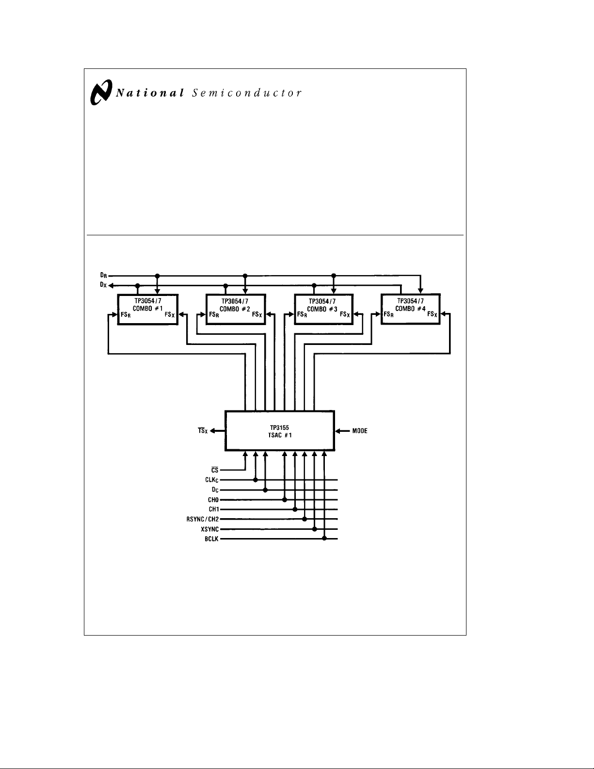
Typical Application
Features
Y
Controls up to 8 COMBO CODEC/Filters
Y
Independent transmit and receive time slot assignments
Y
8-channel unidirectional mode
Y
Up to 32 time slots per frame
Y
Serial control interface compatible with TP3020/TP3021
CODECs
Y
LS TTL and CMOS compatible inputs
Y
5 mW, 5V operation
TL/H/5118– 1
TRI-STATEÉis a registered trademarks of National Semiconductor Corp.
TM
COMBO
is a trademark of National Semiconductor Corp.
C
1995 National Semiconductor Corporation RRD-B30M115/Printed in U. S. A.
TL/H/5118

Absolute Maximum Ratings
If Military/Aerospace specified devices are required,
please contact the National Semiconductor Sales
Office/Distributors for availability and specifications.
V
Relative to GND 7V
CC
Voltage at Any Input
or Output V
a
0.3V to GNDb0.3V
CC
Operating Temperature Range
(Ambient)
Storage Temperature Range
(Ambient)
b
25§Ctoa125§C
b
65§Ctoa150§C
Maximum Lead Temperature
(Soldering, 10 seconds) 300
ESD rating to be determined.
C
§
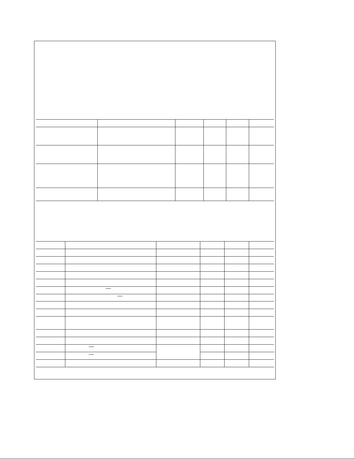
DC Electrical Characteristics
Unless otherwise noted, limits printed in BOLD characters are guaranteed for V
correlation with 100% electrical testing at T
or product design and characterization. Typicals specified at V
e
25§C. All other limits are assured by correlation with other production tests and/
A
CC
e
5.0V, T
A
e
5.0Vg5%; T
CC
e
25§C.
Parameter Conditions Min Typ Max Units
Input Voltage Levels
V
, Logic High 2.0 V
IH
V
, Logic Low 0.7 V
IL
Input Currents
All Inputs Except MODE V
MODE V
k
V
IL
IN
V
IN
0V
IH
e
b
11mA
b
100 mA
k
Output Voltage Levels
V
, Logic High FSXand FSROutputs, I
OH
V
, Logic Low FSXand FSROutputs, I
OL
TS
Output, I
X
e
OL
e
3 mA 2.4 V
OH
e
5 mA 0.4 V
OL
5mA 0.4 V
Power Dissipation BCLKe2.048 MHz, 1 1.5 mA
Operating Current All Outputs Open-Circuit
e
0§Ctoa70§Cby
A
Timing Specifications
Unless otherwise noted, limits printed in BOLD characters are guaranteed for V
correlation with 100% electrical testing at T
or product design and characterization. Typicals specified at V
V
OH
e
2.0V and V
e
0.7V.
OL
e
25§C. All other limits are assured by correlation with other production tests and/
A
CC
e
5.0V, T
A
e
5.0Vg5%, T
CC
e
25§C. All timing parameters are measured at
See Definitions and Timing Conventions section for test methods information.
Symbol Parameter Conditions Min Max Units
t
PC
t
WCH
t
WCL
t
SDC
t
HCD
t
SCC
t
HCC
t
SCHC
t
HCHC
t
DBF
t
HSYNC
t
SSYNC
t
DTL
t
DTH
tRC,t
FC
Period of Clock BCLK, CLK
Width of Clock High BCLK, CLK
Width of Clock Low BCLK, CLK
Set-Up Time from DCto CLK
Hold Time from CLKCto D
Set-Up Time from CS to CLK
C
C
C
C
C
C
480 ns
160 ns
160 ns
50 ns
50 ns
30 ns
Hold Time from CLKCto CS 100 ns
Set-Up Time from Channel Select to CLK
Hold Time from Channel Select to CLK
Delay Time from BCLK Low to FS
High or Low
0–3 C
X/R
C
C
e
50 pF 100 ns
L
50 ns
50 ns
Hold Time from BCLK to Frame Sync 50 ns
Set-Up Time from Frame Sync to BCLK 100 ns
e
50 pF
Delay to TSXLow
Delay to TSXHigh
Rise and Fall Time of Clock BCLK, CLK
C
L
e
R
1k to V
L
CC
C
30 140 ns
e
0§Ctoa70§Cby
A
140 ns
50 ns
2

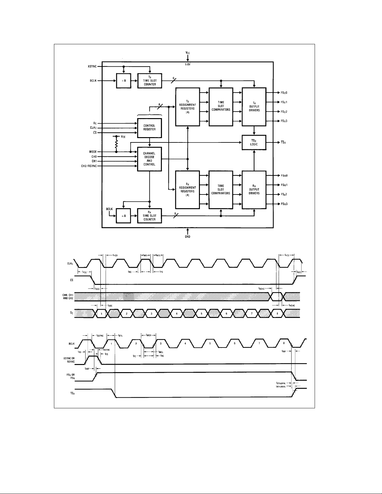
Block Diagram
Timing Diagrams
TL/H/5118– 2
Control Interface
TL/H/5118– 3
Output
TL/H/5118– 4
3
 Loading...