

NATIONAL SEMICONDUCTOR TP3071N-G, TP3071AN-G Datasheet

TP3070, TP3071, TP3070-X
COMBO
®
II Programmable PCM CODEC/Filter
TP3070, TP3071, TP3070-X COMBO II Programmable PCM CODEC/Filter
April 1994
General Description
The TP3070 and TP3071 are second-generation combined
PCM CODEC and Filter devices optimized for digital switching applications on subscriber line and trunk cards. Using
advanced switched capacitor techniques, COMBO II combines transmit bandpass and receive lowpass channel filters
with a companding PCM encoder and decoder. The devices
are A-law and µ-law selectable and employ a conventional
serial PCM interface capable of being clocked up to
4.096 MHz. A number of programmable functions may be
controlled via a serial control port.
Channel gains are programmable over a 25.4 dB range in
each direction, and a programmable filter is included to enable Hybrid Balancing to be adjusted to suit a wide range of
loop impedance conditions. Both transformer and active
SLIC interface circuits with real or complex termination impedances can be balanced by this filter, with cancellation in
excess of 30 dB being readily achievable when measured
across the passband against standard test termination networks.
To enable COMBO II to interface to the SLIC control leads, a
number of programmable latches are included; each may be
configured as either an input or an output. The TP3070 provides 6 latches and the TP3071 5 latches.
Features
n Complete CODEC and FILTER system including:
— Transmit and receive PCM channel filters
— µ-law or A-law companding encoder and decoder
— Receive power amplifier drives 300Ω
— 4.096 MHz serial PCM data (max)
n Programmable Functions:
— Transmit gain: 25.4 dB range, 0.1 dB steps
— Receive gain: 25.4 dB range, 0.1 dB steps
— Hybrid balance cancellation filter
— Time-slot assignment; up to 64 slots/frame
— 2 port assignment (TP3070)
— 6 interface latches (TP3070)
— A or µ-law
— Analog loopback
— Digital loopback
n Direct interface to solid-state SLICs
n Simplifies transformer SLIC; single winding secondary
n Standard serial control interface
n 80 mW operating power (typ)
n 1.5 mW standby power (typ)
n Designed for CCITT and LSSGR applications
n TTL and CMOS compatible digital interfaces
n Extended temperature versions available for −40˚C to
+85˚C (TP3070V-X)
Note: See also AN-614, COMBO II application guide.
COMBO®and TRI-STATE®are registered trademarks of National SemiconductorCorporation.
© 1999 National Semiconductor Corporation DS008635 www.national.com
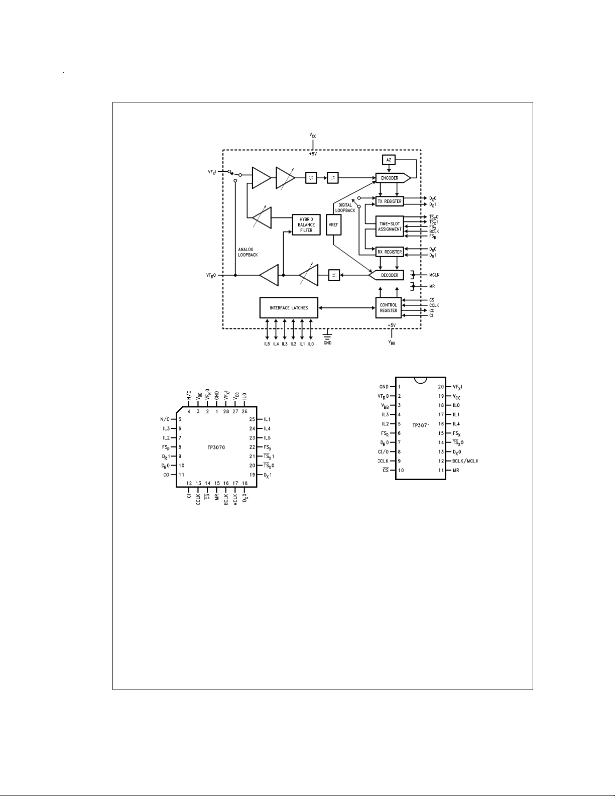
Block Diagram
Connection Diagrams
DS008635-1
FIGURE 1.
DS008635-4
Order Number TP3070V
(0˚C to +70˚C)
Order Number TP3070V-X
(−40˚C to +85˚C)
See NS Package Number V28A
www.national.com 2
DS008635-2
Order Number TP3071J
See NS Package Number J20A
Order Number TP3071N
See NS Package Number N20A
Pin Descriptions
Pin Description
V
V
GND Ground. All analog and digital signals are
FS
+5V±5%power supply.
CC
−5V±5%power supply.
BB
referenced to this pin.
Transmit Frame Sync input. Normally a pulse
X
or squarewave with an 8 kHz repetition rate is
applied to this input to define the start of the
transmit time slot assigned to this device
(non-delayed data timing mode), or the start of
the transmit frame (delayed data timing mode
using the internal time-slot assignment
counter).

Pin Descriptions (Continued)
Pin Description
FS
BCLK Bit clock input used to shift PCM data into and
MCLK Master clock input used by the switched
VF
VF
D
D
TS
TSX1
D
D
CCLK Control Clock input. This clock shifts serial
Receive Frame Sync input. Normally a pulse
R
or squarewave with an 8 kHz repetition rate is
applied to this input to define the start of the
receive time slot assigned to this device
(non-delayed data timing mode), or the start of
the receive frame (delayed data timing mode
using the internal time-slot assignment
counter).
out of the D
from 64 kHz to 4.096 MHz in 8 kHz
and DXpins. BCLK may vary
R
increments, and must be synchronous with
MCLK.
capacitor filters and the encoder and decoder
sequencing logic. Must be 512 kHz, 1.536
MHz, 1.544 MHz, 2.048 MHz or 4.096 MHz
and synchronous with BCLK.
I The Transmit analog high-impedance input.
X
Voice frequency signals present on this input
are encoded as an A-law or µ-law PCM bit
stream and shifted out on the selected D
O The Receive analog power amplifier output,
R
capable of driving load impedances as low as
300Ω (depending on the peak overload level
required). PCM data received on the assigned
pin is decoded and appears at this output
D
R
as voice frequency signals.
D
0
X
1
X
1 is available on the TP3070 only; DX0is
X
available on all devices. These Transmit Data
TRI-STATE
®
outputs remain in the high
impedance state except during the assigned
transmit time slot on the assigned port, during
which the transmit PCM data byte is shifted
out on the rising edges of BCLK.
0
TSX1 is available on the TP3070 only; TSX0is
X
available on all devices. Normally these
open-drain outputs are floating in a high
impedance state except when a time-slot is
active on one of the D
appropriate TS
backplane line-driver.
D
0
R
1
R
1 is available on the TP3070 only; DR0is
R
available on all devices. These receive data
inputs are inactive except during the assigned
outputs, when the
X
output pulls low to enable a
X
receive time slot of the assigned port when
the receive PCM data is shifted in on the
falling edges of BCLK.
control information into or out from CI/O or CI
and CO when the CS input is low, depending
on the current instruction. CCLK may be
asynchronous with the other system clocks.
X
pin.
Pin Description
CI/O This is the Control Data I/O pin which is
provided on the TP3071. Serial control
information is shifted to or read from COMBO
II on this pin when CS is low. The direction of
the data is determined by the current
Table 1
instruction as defined in
.
CI This is a separate Control Input, available only
on the TP3070. It can be connected to CO if
required.
CO This is a separate Control Output, available
only on the TP3070. It can be connected to CI
if required.
CS
Chip Select input. When this pin is low, control
information can be written to or read from
COMBO II via the CI/O pin (or CI and CO).
IL5–IL0 IL5 through IL0 are available on the TP3070.
IL4 through IL0 are available on the TP3071.
Each Interface Latch I/O pin may be
individually programmed as an input or an
output determined by the state of the
corresponding bit in the Latch Direction
Register (LDR). For pins configured as inputs,
the logic state sensed on each input is latched
into the Interface Latch Register (ILR)
whenever control data is written to COMBO II,
while CS is low, and the information is shifted
out on the CO (or CI/O) pin. When configured
as outputs, control data written into the ILR
appears at the corresponding IL pins.
MR This logic input must be pulled low for normal
operation of COMBO II. When pulled
momentarily high (at least 1 µsec.), all
programmable registers in the device are reset
to the states specified under “Power-On
Initialization”.
NC No Connection. Do not connect to this pin. Do
not route traces through this pin.
Functional Description
POWER-ON INITIALIZATION
When power is first applied, power-on reset circuitry initializes the COMBO II and puts it into the power-down state.
The gain control registers for the transmit and receive gain
sections are programmed to OFF (00000000), the hybrid
balance circuit is turned off, the power amp is disabled and
the device is in the non-delayed timing mode. The Latch Direction Register (LDR) is pre-set with all IL pins programmed
as inputs, placing the SLIC interface pins in a high impedance state. The CI/O pin is set as an input ready for the first
control byte of the initialization sequence. Other initial states
in the Control Register are indicated in Section 2.0.
Areset to these same initial conditions may also be forced by
driving the MR pin momentarily high. This may be done either when powered-up or down. For normal operation this
pin must be pulled low.If not used, MR should be hard-wired
to ground.
The desired modes for all programmable functions may be
initialized via the control port prior to a Power-up command.
www.national.com3

Functional Description (Continued)
POWER-DOWN STATE
Following a period of activity in the powered-up state the
power-down state may be re-entered by writing any of the
control instructions into the serial control port with the “P” bit
set to “1” as indicated in
chip be powered down before writing any additional instructions. In the power-down state, all non-essential circuitry is
de-activated and the D
impedance TRI-STATE condition.
The coefficients stored in the Hybrid Balance circuit and the
Gain Control registers, the data in the LDR and ILR, and all
control bits remain unchanged in the power-down state unless changed by writing new data via the serial control port,
which remains active. The outputs of the Interface Latches
also remain active, maintaining the ability to monitor and
control the SLIC.
TRANSMIT FILTER AND ENCODER
The Transmit section input, VF
ming input which is used as the differencing point for the internal hybrid balance cancellation signal. No external components are necessary to set the gain. Following this circuit
is a programmable gain/attenuation amplifier which is controlled by the contents of the Transmit Gain Register (see
Programmable Functions section). An active pre-filter then
precedes the 3rd order high-pass and 5th order low-pass
switched capacitor filters. The A/D converter has a compressing characteristic according to the standard CCITT A or
µ255 coding laws, which must be selected by a control instruction during initialization (see
cision on-chip voltage reference ensures accurate and highly
stable transmission levels. Any offset voltage arising in the
gain-set amplifier,the filters or the comparator is canceled by
an internal auto-zero circuit.
Each encode cycle begins immediately following the assigned Transmit time-slot. The total signal delay referenced
to the start of the time-slot is approximately 165 µs (due to
the Transmit Filter) plus 125 µs (due to encoding delay),
which totals 290 µs. Data is shifted out on D
the selected time slot on eight rising edges of BCLK.
DECODER AND RECEIVE FILTER
PCM data is shifted into the Decoder’s Receive PCM Register via the D
the 8 falling edges of BCLK. The Decoder consists of an ex-
0orDR1 pin during the selected time-slot on
R
panding DAC with either A or µ255 law decoding characteristic, which is selected by the same control instruction used
to select the Encode law during initialization. Following the
Decoder is a 5th order low-pass switched capacitor filter with
integral Sin x/x correction for the 8 kHz sample and hold. A
programmable gain amplifier, which must be set by writing to
the Receive Gain Register, is included, and finally a Power
Amplifier capable of driving a 300Ω load to
±
load to
3.8V or a 15 kΩ load to±4.0V at peak overload.
Table1
. It is recommended that the
0 (and DX1) outputs are in the high
X
I, is a high impedance sum-
X
Table1
and
Table2
).A pre-
0orDX1 during
X
±
3.5V, a 600Ω
A decode cycle begins immediately after the assigned receive time-slot, and 10 µs later the Decoder DAC output is
updated. The total signal delay is 10 µs plus 120 µs (filter delay) plus 62.5 µs (
1
⁄2frame) which gives approximately 190
µs.
PCM INTERFACE
The FS
ning of the 8-bit transmit and receive time-slots respectively.
and FSRframe sync inputs determine the begin-
X
They may have any duration from a single cycle of BCLK
HIGH to one MCLK period LOW. Two different relationships
may be established between the frame sync inputs and the
actual time-slots on the PCM busses by setting bit 3 in the
Control Register (see
Table 2
). Non-delayed data mode is
similar to long-frame timing on the TP3050/60 series of devices (COMBO); time-slots begin nominally coincident with
the rising edge of the appropriate FS input. The alternative is
to use Delayed Data mode, which is similar to short-frame
sync timing on COMBO, in which each FS input must be high
at least a half-cycle of BCLK earlier than the time-slot. The
Time-SlotAssignment circuit on the device can only be used
with Delayed Data timing.
When using Time-SlotAssignment, the beginning of the first
time-slot in a frame is identified by the appropriate FS input.
The actual transmit and receive time-slots are then determined by the internal Time-Slot Assignment counters.
Transmit and Receive frames and time-slots may be skewed
from each other by any number of BCLK cycles. During each
assigned Transmit time-slot, the selected D
data out from the PCM register on the rising edges of BCLK.
TS
0 (or TSX1 as appropriate) also pulls low for the first 71⁄
X
bit times of the time-slot to control the TRI-STATE Enable of
0/1 output shifts
X
a backplane line-driver. Serial PCM data is shifted into the
selected D
on the falling edges of BCLK. D
are selectable on the TP3070 only, see Section 6.
0/1 input during each assigned Receive time-slot
R
0orDX1 and DR0orDR1
X
2
www.national.com 4

Functional Description (Continued)
TABLE 1. Programmable Register Instructions
Function Byte 1 (Note 1) Byte 2 (Note 1)
76543210 76543210
Single Byte Power-Up/Down PXXXXX0X None
Write Control Register P 000001X See
Read-Back Control Register P 000011X See
Write to Interface Latch Register P 000101X See
Read Interface Latch Register P 000111X See
Write Latch Direction Register P 001001X See
Read Latch Direction Register P 001011X See
Write Receive Gain Register P 010001X See
Read Receive Gain Register P 010011X See
Write Transmit Gain Register P 010101X See
Read Transmit Gain Register P 010111X See
Write Receive Time-Slot/Port P 100101X See
Read-Back Receive Time-Slot/Port P 100111X See
Write Transmit Time-Slot/Port P 101001X See
Read-Back Transmit Time-Slot/Port P 101011X See
Write Hybrid Balance Register 1 P 011001X
Read Hybrid Balance Register 1 P 011011X
Write Hybrid Balance Register 2 P 011101X
Read Hybrid Balance Register 2 P 011111X
Write Hybrid Balance Register 3 P 100001X
Read Hybrid Balance Register 3 P 100011X
Note 1: Bit 7 of bytes 1 and 2 is always the first bit clocked into or out from the CI, CO or CI/O pin. X=don’t care.
Note 2: “P” is the power-up/down control bit, see “Power-Up/Down Control” section. (“0”=Power Up, “1”=Power Down)
Note 3: Other register address codes are invalid and should not be used.
Table 2
Table 2
Table 4
Table 4
Table 3
Table 3
Table 8
Table 8
Table 7
Table 7
Table 6
Table 6
Table 6
Table 6
Derive from
Optimization
Routine in
TP3077SW
Program
SERIAL CONTROL PORT
Control information and data are written into or read-back
from COMBO II via the serial control port consisting of the
control clock CCLK, the serial data input/output CI/O, (or
separate input, CI, and output, CO, on the TP3070 only), and
the Chip Select input, CS. All control instructions require 2
bytes, as listed in
power-up/down command. The byte 1 bits are used as follows: bit 7 specifies power up or power down; bits 6, 5, 4 and
3 specify the register address; bit 2 specifies whether the instruction is read or write; bit 1 specifies a one or two byte instruction; and bit 0 is not used.
To shift control data into COMBO II, CCLK must be pulsed 8
times while CS is low. Data on the CI/O (or CI) input is
shifted into the serial input register on the falling edge of
each CCLK pulse. After all data is shifted in, the contents of
the input shift register are decoded, and may indicate that a
2nd byte of control data will follow. This second byte may either be defined by a second byte-wide CS pulse or may follow the first contiguously, i.e. it is not mandatory for CS to return high between the first and second control bytes. At the
end of CCLK8 in the 2nd control byte the data is loaded into
the appropriate programmable register. CS may remain low
continuously when programming successive registers, if desired. However, CS should be set high when no data transfers are in progress.
To readback Interface Latch data or status information from
COMBO II, the first byte of the appropriate instruction is
Table1
, with the exception of a single byte
strobed in while CS is low, as defined in
kept low, or be taken low again for a further 8 CCLK cycles,
during which the data is shifted onto the CO or CI/O pin on
the rising edges of CCLK. When CS is high the CO or CI/O
pin is in the high-impedance TRI-STATE, enabling the CI/O
pins of many devices to be multiplexed together.
If CS returns high during either byte 1 or byte 2 before all
eight CCLK pulses of that byte occur, both the bit count and
byte count are reset and register contents are not affected.
This prevents loss of synchronization in the control interface
as well as corruption of register data due to processor interrupt or other problem. When CS returns low again, the device will be ready to accept bit 1 of byte 1 of a new instruction.
Table1
. CS must be
Programmable Functions
1.0 POWER-UP/DOWN CONTROL
Following power-on initialization, power-up and power-down
control may be accomplished by writing any of the control instructions listed in
to “0” for power-up or “1” for power-down. Normally it is recommended that all programmable functions be initially programmed while the device is powered down. Power state
control can then be included with the last programming instruction or the separate single-byte instruction. Any of the
programmable registers may also be modified while the de-
Table1
into COMBO II with the “P” bit set
www.national.com5
Programmable Functions (Continued)
vice is powered-up or down by setting the “P” bit as indicated. When the power-up or down control is entered as a
single byte instruction, bit one (1) must be reset to a 0.
When a power-up command is given, all de-activated circuits
are activated, but the TRI-STATE PCM output(s), D
D
1), will remain in the high impedance state until the sec-
X
ond FS
pulse after power-up.
X
2.0 CONTROL REGISTER INSTRUCTION
The first byte of a READ or WRITE instruction to the Control
Register is as shown in
Table1
. The second byte has the fol-
lowing bit functions:
TABLE 2. Control Register Byte 2 Functions
Bit Number and Name
76 5 43210 Function
MA IA DN DL AL PP
F
1F0
0 0 MCLK=512 kHz
0 1 MCLK=1.536
1 0 MCLK=2.048 MHz
1 1 MCLK=4.096 MHz
0 X Select µ-255 law (Note 4)
1 0 A-law, Including Even
1 1 A-law, No Even Bit Inversion
0 Delayed Data Timing
1 Non-Delayed Data
0 0 Normal Operation
1 X Digital Loopback
0 1 Analog Loopback
Note 4: State at power-on initialization. (Bit 4=0)
or 1.544 MHz
(Note 4)
Bit Inversion
Timing (Note 4)
(Note 4)
0 Power Amp Enabled in PDN
1 Power Amp Disabled in
PDN (Note 4)
2.1 Master Clock Frequency Selection
A Master clock must be provided to COMBO II for operation
of the filter and coding/decoding functions. The MCLK frequency must be either 512 kHz, 1.536 MHz, 1.544 MHz,
2.048 MHz, or 4.096 MHz and must be synchronous with
BCLK. Bits F
ization to select the correct internal divider.
and F0(see
1
Table2
) must be set during initial-
2.2 Coding Law Selection
Bits “MA” and “IA” in
Table 2
permit the selection of µ255
coding or A-law coding, with or without even bit inversion.
2.3 Analog Loopback
Analog Loopback mode is entered by setting the “AL” and
“DL” bits in the Control Register as shown in
analog loopback mode, the Transmit input VF
from the input pin and internally connected to the VF
put, forming a loop from the Receive PCM Register back to
the Transmit PCM Register. The VF
and the programmed settings of the Transmit and Receive
O pin remains active,
R
Table 2
I is isolated
X
0 (and
X
.Inthe
O out-
R
gains remain unchanged, thus care must be taken to ensure
that overload levels are not exceeded anywhere in the loop.
Hybrid balance must be disabled for meaningful analog loopback function.
2.4 Digital Loopback
Digital Loopback mode is entered by setting the “AL” and
“DL” bits in the Control Register as shown in
Table 2
. This
mode provides another stage of path verification by enabling
data written into the Receive PCM Register to be read back
from that register in any Transmit time-slot at D
loopback, the decoder will remain functional and output a
signal at VF
be turned off by programming the receive gain register to all
O. If this is undesirable, the receive output can
R
0/1. In digital
X
zeros.
3.0 INTERFACE LATCH DIRECTIONS
Immediately following power-on, all Interface Latches assume they are inputs, and therefore all IL pins are in a high
impedance state. Each IL pin may be individually programmed as a logic input or output by writing the appropriate
instruction to the LDR, see
Table 1
and
Table 3
. For minimum power dissipation, unconnected latch pins should be
programmed as outputs. For the TP3071, L5 should always
be programmed as an output.
Bits L
the LDR with the L bits in the second byte set as follows:
must be set by writing the specified instruction to
5–L0
TABLE 3. Byte 2 Functions of Latch Direction Register
Byte 2 Bit Number
76543210
L
L1L2L3L4L5XX
0
LnBit IL Direction
0 Input
1 Output
X=don’t care
INTERFACE LATCH STATES
Interface Latches configured as outputs assume the state
determined by the appropriate data bit in the 2-byte instruction written to the Interface Latch Register (ILR) as shown in
Table1
and
Table4
. Latches configured as inputs will sense
the state applied by an external source, such as the
Off-Hook detect output of a SLIC. All bits of the ILR, i.e.
sensed inputs and the programmed state of outputs, can be
read back in the 2nd byte of a READ from the ILR.
It is recommended that during initialization, the state of IL
pins to be configured as outputs should be programmed first,
followed immediately by the Latch Direction Register.
TABLE 4. Interface Latch Data Bit Order
Bit Number
76543210
D
D1D2D3D4D5XX
0
www.national.com 6
Programmable Functions (Continued)
TABLE 5. Coding Law Conventions
µ255 law
MSB LSB MSB LSB MSB LSB
=
V
+Full Scale 10000000 10101010 11111111
IN
=
V
0V 11111111 11010101 10000000
IN
01111111 01010101 00000000
=
V
−Full Scale 00000000 00101010 01111111
IN
Note 5: The MSB is always the first PCM bit shifted in or out of COMBO II.
TABLE 6. Time-Slot and Port Assignment Instruction
Bit Number and Name Function
7 6 5 43210
EN PS T
5
T
T
4
T
3
2
(Note 6) (Note 7)
0 0 X XXXXXDisable D
0 1 X XXXXXDisable D
1 0 Assign One Binary Coded Time-Slot from 0–63 Enable D
Assign One Binary Coded Time-Slot from 0–63 Enable D
1 1 Assign One Binary Coded Time-Slot from 0–63 Enable D
Assign One Binary Coded Time-Slot from 0–63 Enable D
Note 6: The “PS” bit MUST always be set to 0 for the TP3071.
Note 7: T5 is the MSB of the Time-slot assignment bit field. Time slot bits should be set to “000000” for both transmit and receive when operating in non-delayed
data timing mode.
True A-law with A-law without
even bit inversion even bit inversion
T
T
1
0
0 Output (Transmit Instruction)
Disable D
Disable D
X
0 Input (Receive Instruction)
R
1 Output (Transmit Instruction)
X
1 Input (Receive Instruction)
R
0 Output (Transmit Instruction)
X
0 Input (Receive Instruction)
R
1 Output (Transmit Instruction)
X
1 Input (Receive Instruction)
R
5.0 TIME-SLOT ASSIGNMENT
COMBO II can operate in either fixed time-slot or time-slot
assignment mode for selecting the Transmit and Receive
PCM time-slots. Following power-on, the device is automatically in Non-Delayed Timing mode, in which the time-slot always begins with the leading (rising) edge of frame sync inputs FS
and FSR. Time-Slot Assignment may only be used
X
with Delayed Data timing; see
Figure 5
.FSXand FSRmay
have any phase relationship with each other in BCLK period
increments.
Alternatively, the internal time-slot assignment counters and
comparators can be used to access any time-slot in a frame,
using the frame sync inputs as marker pulses for the beginning of transmit and receive time-slot 0. In this mode, a
frame may consist of up to 64 time-slots of 8 bits each. A
time-slot is assigned by a 2-byte instruction as shown in
Table 1
and
Table 6
. The last 6 bits of the second byte indicate the selected time-slot from 0–63 using straight binary
notation. When writing a timeslot and port assignment register, if the PCM interface is currently active, it is immediately
deactivated to prevent possible bus clashes. A new assignment becomes active on the second frame following the end
of the Chip-Select for the second control byte. Rewriting of
register contents should not be performed during the talking
period of a connection to prevent waveform distortion
caused by loss of a sample which will occur with each register write. The “EN” bit allows the PCM inputs, D
puts, D
0/1, as appropriate, to be enabled or disabled.
X
0/1, or out-
R
Time-Slot Assignment mode requires that the FS
pulses must conform to the delayed data timing format
shown in
Figure 5
.
and FS
X
6.0 PORT SELECTION
On the TP3070 only, an additional capability is available; 2
Transmit serial PCM ports, D
rial PCM ports, D
two-way space switching to be implemented. Port selections
R
0 and DX1, and 2 Receive se-
X
0 and DR1, are provided to enable
for transmit and receive are made within the appropriate
time-slot assignment instruction using the “PS” bit in the second byte. The PS bit selects either Port 0 or Port 1. Both
ports cannot be active at the same time.
On the TP3071, only ports D
fore the “PS” bit MUST always be set to 0 for these devices.
Table 6
shows the format for the second byte of both trans-
0 and DR0 are available, there-
X
mit and receive time-slot and port assignment instructions.
7.0 TRANSMIT GAIN INSTRUCTION BYTE 2
The transmit gain can be programmed in 0.1 dB steps by
writing to the Transmit Gain Register as defined in
and
Table7
VF
+6.4 dBm to −19.0 dBm in 600Ω).
. This corresponds to a range of 0 dBm0 levels at
I between 1.619 Vrms and 0.087 Vrms (equivalent to
X
Table 1
To calculate the binary code for byte 2 of this instruction for
any desired input 0 dBm0 level in Vrms, take the nearest integer to the decimal number given by:
200 x log
(V/0.08595)
10
www.national.com7
R

Programmable Functions (Continued)
and convert to the binary equivalent. Some examples are
given in
Table7
dix I of AN-614.
It should be noted that the Transmit (idle channel) Noise and
Transmit Signal to Total Distortion are both specified with
transmit gain set to 0 dB (Gain Register set to all ones). At
high transmit gains there will be some degradation in noise
performance for these parameters. See Application Note
AN-614 for more information on this subject.
TABLE 7. Byte 2 of Transmit Gain Instruction
Bit Number 0 dBm0 Test Level (Vrms)
76543210 atVF
00000000 NoOutput (Note 8)
00000001 0.087
00000010 0.088
11111110 1.600
11111111 1.619
Note 8: Analog signal path is cut off, but DXremains active and will output
codes representing idle noise.
8.0 RECEIVE GAIN INSTRUCTION BYTE 2
The receive gain can be programmed in 0.1 dB steps by writing to the Receive Gain Register as defined in
Table8
bility:
a) 0 dBm0 levels ≤ 1.96 Vrms at VF
a load of ≥ 15 kΩ to GND; receive gain set to 0 dB (Gain
Register set to all ones)
b) 0 dBm0 levels ≤ 1.85 Vrms at VF
a load of ≥ 600Ω to GND; receive gain set to −0.5 dB
c) 0 dBm0 levels ≤ 1.71 Vrms at VF
a load of ≥ 300Ω to GND; receive gain set to −1.2 dB
To calculate the binary code for byte 2 of this instruction for
any desired output 0 dBm0 level in Vrms, take the nearest integer to the decimal number given by:
and convert to the binary equivalent. Some examples are
given in
dix I of AN-614.
TABLE 8. Byte 2 of Receive Gain Instruction
Bit Number 0 dBm0 Test Level (Vrms)
76543210 atVF
00000000 NoOutput (Low Z to GND)
00000001 0.105
00000010 0.107
11111110 1.941
11111111 1.964
9.0 HYBRID BALANCE FILTER
The Hybrid Balance Filter on COMBO II is a programmable
filter consisting of a second-order section, Hybal1, followed
by a first-order section, Hybal2, and a programmable attenu-
www.national.com 8
and a complete tabulation is given in Appen-
I
X
——
Table 1
and
. Note the following restrictions on output drive capa-
O may be driven into
R
O may be driven into
R
O may be driven into
R
200 x log
Table8
and a complete tabulation is given in Appen-
(V/0.1043)
10
O
R
——
ator. Either of the filter sections can be bypassed if only one
is required to achieve good cancellation. A selectable 180
degree inverting stage is included to compensate for interface circuits which also invert the transmit input relative to
the receive output signal. The 2nd order section is intended
mainly to balance low frequency signals across a transformer SLIC, and the first order section to balance midrange
to higher audio frequency signals.
As a 2nd order section, Hybal1 has a pair of low frequency
zeroes and a pair of complex conjugate poles. When configuring Hybal1, matching the phase of the hybrid at low to
mid-band frequencies is most critical. Once the echo path is
correctly balanced in phase, the magnitude of the cancellation signal can be corrected by the programmable attenuator.
The 2nd order mode of Hybal1 is most suitable for balancing
interfaces with transformers having high inductance of 1.5
Henries or more. An alternative configuration for smaller
transformers is available by converting Hybal1 to a simple
first-order section with a single real low-frequency pole and
zero. In this mode, the pole/zero frequency may be programmed.
Many line interfaces can be adequately balanced by use of
the Hybal1 section only, in which case the Hybal2 filter
should be de-selected to bypass it.
Hybal2, the higher frequency first-order section, is provided
for balancing an electronic SLIC, and is also helpful with a
transformer SLIC in providing additional phase correction for
mid and high-band frequencies, typically 1 kHz to 3.4 kHz.
Such a correction is particularly useful if the test balance impedance includes a capacitor of 100 nF or less, such as the
loaded and non-loaded loop test networks in the United
States. Independent placement of the pole and zero location
is provided.
Figure 2
shows a simplified diagram of the local echo path
for a typical application with a transformer interface. The
magnitude and phase of the local echo signal, measured at
VF
I, are a function of the termination impedance ZT, the line
X
transformer and the impedance of the 2W loop, Z
pedance reflected back into the transformer primary is expressed as Z
VF
OtoVFXI is:
R
' then the echo path transfer function from
L
H(w)=Z
'/(ZT+ZL') (1)
L
. If the im-
L
9.1 PROGRAMMING THE FILTER
On initial power-up, the Hybrid Balance filter is disabled. Before the hybrid balance filter can be programmed it is necessary to design the transformer and termination impedance in
order to meet system 2W input return loss specifications,
which are normally measured against a fixed test impedance
(600 or 900Ω in most countries). Only then can the echo
path be modeled and the hybrid balance filter programmed.
Hybrid balancing is also measured against a fixed test impedance, specified by each national Telecom administration
to provide adequate control of talker and listener echo over
the majority of their network connections. This test impedance is Z
transhybrid loss obtained by the programmable filter must be
measured from the PCM digital input, D
tal output, D
conversion back to analog by a PCM CODEC/Filter.
in
Figure 2
L
X
. The echo signal and the degree of
0, to the PCM digi-
0, either by digital test signal analysis or by
R
 Loading...