

Page 1

TP3070, TP3071, TP3070-X
COMBO
®
II Programmable PCM CODEC/Filter
TP3070, TP3071, TP3070-X COMBO II Programmable PCM CODEC/Filter
April 1994
General Description
The TP3070 and TP3071 are second-generation combined
PCM CODEC and Filter devices optimized for digital switching applications on subscriber line and trunk cards. Using
advanced switched capacitor techniques, COMBO II combines transmit bandpass and receive lowpass channel filters
with a companding PCM encoder and decoder. The devices
are A-law and µ-law selectable and employ a conventional
serial PCM interface capable of being clocked up to
4.096 MHz. A number of programmable functions may be
controlled via a serial control port.
Channel gains are programmable over a 25.4 dB range in
each direction, and a programmable filter is included to enable Hybrid Balancing to be adjusted to suit a wide range of
loop impedance conditions. Both transformer and active
SLIC interface circuits with real or complex termination impedances can be balanced by this filter, with cancellation in
excess of 30 dB being readily achievable when measured
across the passband against standard test termination networks.
To enable COMBO II to interface to the SLIC control leads, a
number of programmable latches are included; each may be
configured as either an input or an output. The TP3070 provides 6 latches and the TP3071 5 latches.
Features
n Complete CODEC and FILTER system including:
— Transmit and receive PCM channel filters
— µ-law or A-law companding encoder and decoder
— Receive power amplifier drives 300Ω
— 4.096 MHz serial PCM data (max)
n Programmable Functions:
— Transmit gain: 25.4 dB range, 0.1 dB steps
— Receive gain: 25.4 dB range, 0.1 dB steps
— Hybrid balance cancellation filter
— Time-slot assignment; up to 64 slots/frame
— 2 port assignment (TP3070)
— 6 interface latches (TP3070)
— A or µ-law
— Analog loopback
— Digital loopback
n Direct interface to solid-state SLICs
n Simplifies transformer SLIC; single winding secondary
n Standard serial control interface
n 80 mW operating power (typ)
n 1.5 mW standby power (typ)
n Designed for CCITT and LSSGR applications
n TTL and CMOS compatible digital interfaces
n Extended temperature versions available for −40˚C to
+85˚C (TP3070V-X)
Note: See also AN-614, COMBO II application guide.
COMBO®and TRI-STATE®are registered trademarks of National SemiconductorCorporation.
© 1999 National Semiconductor Corporation DS008635 www.national.com
Page 2
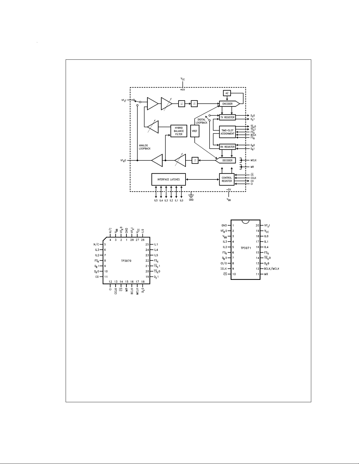
Block Diagram
Connection Diagrams
DS008635-1
FIGURE 1.
DS008635-4
Order Number TP3070V
(0˚C to +70˚C)
Order Number TP3070V-X
(−40˚C to +85˚C)
See NS Package Number V28A
www.national.com 2
DS008635-2
Order Number TP3071J
See NS Package Number J20A
Order Number TP3071N
See NS Package Number N20A
Pin Descriptions
Pin Description
V
V
GND Ground. All analog and digital signals are
FS
+5V±5%power supply.
CC
−5V±5%power supply.
BB
referenced to this pin.
Transmit Frame Sync input. Normally a pulse
X
or squarewave with an 8 kHz repetition rate is
applied to this input to define the start of the
transmit time slot assigned to this device
(non-delayed data timing mode), or the start of
the transmit frame (delayed data timing mode
using the internal time-slot assignment
counter).
Page 3

Pin Descriptions (Continued)
Pin Description
FS
BCLK Bit clock input used to shift PCM data into and
MCLK Master clock input used by the switched
VF
VF
D
D
TS
TSX1
D
D
CCLK Control Clock input. This clock shifts serial
Receive Frame Sync input. Normally a pulse
R
or squarewave with an 8 kHz repetition rate is
applied to this input to define the start of the
receive time slot assigned to this device
(non-delayed data timing mode), or the start of
the receive frame (delayed data timing mode
using the internal time-slot assignment
counter).
out of the D
from 64 kHz to 4.096 MHz in 8 kHz
and DXpins. BCLK may vary
R
increments, and must be synchronous with
MCLK.
capacitor filters and the encoder and decoder
sequencing logic. Must be 512 kHz, 1.536
MHz, 1.544 MHz, 2.048 MHz or 4.096 MHz
and synchronous with BCLK.
I The Transmit analog high-impedance input.
X
Voice frequency signals present on this input
are encoded as an A-law or µ-law PCM bit
stream and shifted out on the selected D
O The Receive analog power amplifier output,
R
capable of driving load impedances as low as
300Ω (depending on the peak overload level
required). PCM data received on the assigned
pin is decoded and appears at this output
D
R
as voice frequency signals.
D
0
X
1
X
1 is available on the TP3070 only; DX0is
X
available on all devices. These Transmit Data
TRI-STATE
®
outputs remain in the high
impedance state except during the assigned
transmit time slot on the assigned port, during
which the transmit PCM data byte is shifted
out on the rising edges of BCLK.
0
TSX1 is available on the TP3070 only; TSX0is
X
available on all devices. Normally these
open-drain outputs are floating in a high
impedance state except when a time-slot is
active on one of the D
appropriate TS
backplane line-driver.
D
0
R
1
R
1 is available on the TP3070 only; DR0is
R
available on all devices. These receive data
inputs are inactive except during the assigned
outputs, when the
X
output pulls low to enable a
X
receive time slot of the assigned port when
the receive PCM data is shifted in on the
falling edges of BCLK.
control information into or out from CI/O or CI
and CO when the CS input is low, depending
on the current instruction. CCLK may be
asynchronous with the other system clocks.
X
pin.
Pin Description
CI/O This is the Control Data I/O pin which is
provided on the TP3071. Serial control
information is shifted to or read from COMBO
II on this pin when CS is low. The direction of
the data is determined by the current
Table 1
instruction as defined in
.
CI This is a separate Control Input, available only
on the TP3070. It can be connected to CO if
required.
CO This is a separate Control Output, available
only on the TP3070. It can be connected to CI
if required.
CS
Chip Select input. When this pin is low, control
information can be written to or read from
COMBO II via the CI/O pin (or CI and CO).
IL5–IL0 IL5 through IL0 are available on the TP3070.
IL4 through IL0 are available on the TP3071.
Each Interface Latch I/O pin may be
individually programmed as an input or an
output determined by the state of the
corresponding bit in the Latch Direction
Register (LDR). For pins configured as inputs,
the logic state sensed on each input is latched
into the Interface Latch Register (ILR)
whenever control data is written to COMBO II,
while CS is low, and the information is shifted
out on the CO (or CI/O) pin. When configured
as outputs, control data written into the ILR
appears at the corresponding IL pins.
MR This logic input must be pulled low for normal
operation of COMBO II. When pulled
momentarily high (at least 1 µsec.), all
programmable registers in the device are reset
to the states specified under “Power-On
Initialization”.
NC No Connection. Do not connect to this pin. Do
not route traces through this pin.
Functional Description
POWER-ON INITIALIZATION
When power is first applied, power-on reset circuitry initializes the COMBO II and puts it into the power-down state.
The gain control registers for the transmit and receive gain
sections are programmed to OFF (00000000), the hybrid
balance circuit is turned off, the power amp is disabled and
the device is in the non-delayed timing mode. The Latch Direction Register (LDR) is pre-set with all IL pins programmed
as inputs, placing the SLIC interface pins in a high impedance state. The CI/O pin is set as an input ready for the first
control byte of the initialization sequence. Other initial states
in the Control Register are indicated in Section 2.0.
Areset to these same initial conditions may also be forced by
driving the MR pin momentarily high. This may be done either when powered-up or down. For normal operation this
pin must be pulled low.If not used, MR should be hard-wired
to ground.
The desired modes for all programmable functions may be
initialized via the control port prior to a Power-up command.
www.national.com3
Page 4

Functional Description (Continued)
POWER-DOWN STATE
Following a period of activity in the powered-up state the
power-down state may be re-entered by writing any of the
control instructions into the serial control port with the “P” bit
set to “1” as indicated in
chip be powered down before writing any additional instructions. In the power-down state, all non-essential circuitry is
de-activated and the D
impedance TRI-STATE condition.
The coefficients stored in the Hybrid Balance circuit and the
Gain Control registers, the data in the LDR and ILR, and all
control bits remain unchanged in the power-down state unless changed by writing new data via the serial control port,
which remains active. The outputs of the Interface Latches
also remain active, maintaining the ability to monitor and
control the SLIC.
TRANSMIT FILTER AND ENCODER
The Transmit section input, VF
ming input which is used as the differencing point for the internal hybrid balance cancellation signal. No external components are necessary to set the gain. Following this circuit
is a programmable gain/attenuation amplifier which is controlled by the contents of the Transmit Gain Register (see
Programmable Functions section). An active pre-filter then
precedes the 3rd order high-pass and 5th order low-pass
switched capacitor filters. The A/D converter has a compressing characteristic according to the standard CCITT A or
µ255 coding laws, which must be selected by a control instruction during initialization (see
cision on-chip voltage reference ensures accurate and highly
stable transmission levels. Any offset voltage arising in the
gain-set amplifier,the filters or the comparator is canceled by
an internal auto-zero circuit.
Each encode cycle begins immediately following the assigned Transmit time-slot. The total signal delay referenced
to the start of the time-slot is approximately 165 µs (due to
the Transmit Filter) plus 125 µs (due to encoding delay),
which totals 290 µs. Data is shifted out on D
the selected time slot on eight rising edges of BCLK.
DECODER AND RECEIVE FILTER
PCM data is shifted into the Decoder’s Receive PCM Register via the D
the 8 falling edges of BCLK. The Decoder consists of an ex-
0orDR1 pin during the selected time-slot on
R
panding DAC with either A or µ255 law decoding characteristic, which is selected by the same control instruction used
to select the Encode law during initialization. Following the
Decoder is a 5th order low-pass switched capacitor filter with
integral Sin x/x correction for the 8 kHz sample and hold. A
programmable gain amplifier, which must be set by writing to
the Receive Gain Register, is included, and finally a Power
Amplifier capable of driving a 300Ω load to
±
load to
3.8V or a 15 kΩ load to±4.0V at peak overload.
Table1
. It is recommended that the
0 (and DX1) outputs are in the high
X
I, is a high impedance sum-
X
Table1
and
Table2
).A pre-
0orDX1 during
X
±
3.5V, a 600Ω
A decode cycle begins immediately after the assigned receive time-slot, and 10 µs later the Decoder DAC output is
updated. The total signal delay is 10 µs plus 120 µs (filter delay) plus 62.5 µs (
1
⁄2frame) which gives approximately 190
µs.
PCM INTERFACE
The FS
ning of the 8-bit transmit and receive time-slots respectively.
and FSRframe sync inputs determine the begin-
X
They may have any duration from a single cycle of BCLK
HIGH to one MCLK period LOW. Two different relationships
may be established between the frame sync inputs and the
actual time-slots on the PCM busses by setting bit 3 in the
Control Register (see
Table 2
). Non-delayed data mode is
similar to long-frame timing on the TP3050/60 series of devices (COMBO); time-slots begin nominally coincident with
the rising edge of the appropriate FS input. The alternative is
to use Delayed Data mode, which is similar to short-frame
sync timing on COMBO, in which each FS input must be high
at least a half-cycle of BCLK earlier than the time-slot. The
Time-SlotAssignment circuit on the device can only be used
with Delayed Data timing.
When using Time-SlotAssignment, the beginning of the first
time-slot in a frame is identified by the appropriate FS input.
The actual transmit and receive time-slots are then determined by the internal Time-Slot Assignment counters.
Transmit and Receive frames and time-slots may be skewed
from each other by any number of BCLK cycles. During each
assigned Transmit time-slot, the selected D
data out from the PCM register on the rising edges of BCLK.
TS
0 (or TSX1 as appropriate) also pulls low for the first 71⁄
X
bit times of the time-slot to control the TRI-STATE Enable of
0/1 output shifts
X
a backplane line-driver. Serial PCM data is shifted into the
selected D
on the falling edges of BCLK. D
are selectable on the TP3070 only, see Section 6.
0/1 input during each assigned Receive time-slot
R
0orDX1 and DR0orDR1
X
2
www.national.com 4
Page 5
Functional Description (Continued)
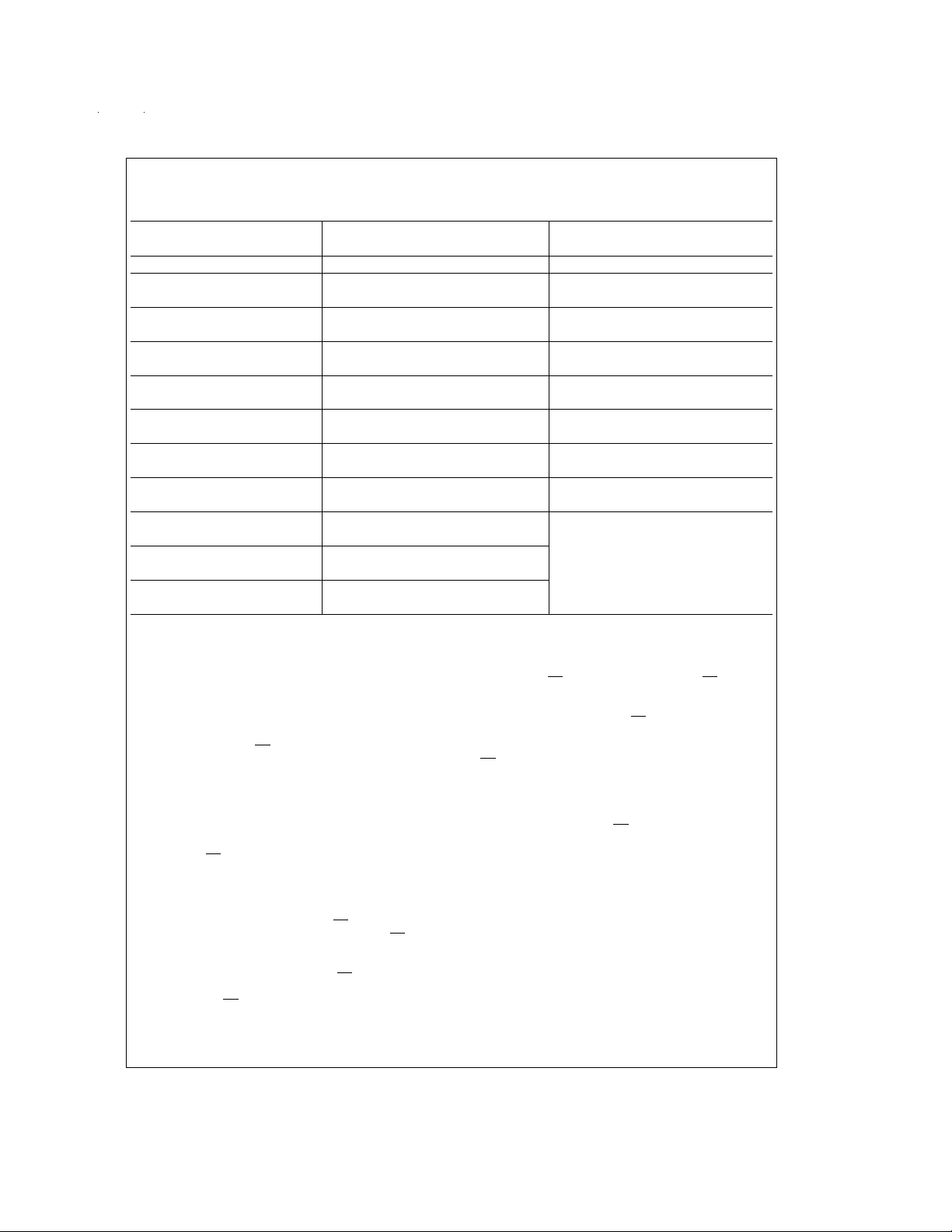
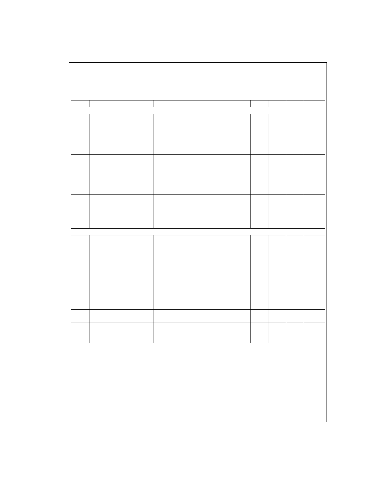
TABLE 1. Programmable Register Instructions
Function Byte 1 (Note 1) Byte 2 (Note 1)
76543210 76543210
Single Byte Power-Up/Down PXXXXX0X None
Write Control Register P 000001X See
Read-Back Control Register P 000011X See
Write to Interface Latch Register P 000101X See
Read Interface Latch Register P 000111X See
Write Latch Direction Register P 001001X See
Read Latch Direction Register P 001011X See
Write Receive Gain Register P 010001X See
Read Receive Gain Register P 010011X See
Write Transmit Gain Register P 010101X See
Read Transmit Gain Register P 010111X See
Write Receive Time-Slot/Port P 100101X See
Read-Back Receive Time-Slot/Port P 100111X See
Write Transmit Time-Slot/Port P 101001X See
Read-Back Transmit Time-Slot/Port P 101011X See
Write Hybrid Balance Register 1 P 011001X
Read Hybrid Balance Register 1 P 011011X
Write Hybrid Balance Register 2 P 011101X
Read Hybrid Balance Register 2 P 011111X
Write Hybrid Balance Register 3 P 100001X
Read Hybrid Balance Register 3 P 100011X
Note 1: Bit 7 of bytes 1 and 2 is always the first bit clocked into or out from the CI, CO or CI/O pin. X=don’t care.
Note 2: “P” is the power-up/down control bit, see “Power-Up/Down Control” section. (“0”=Power Up, “1”=Power Down)
Note 3: Other register address codes are invalid and should not be used.
Table 2
Table 2
Table 4
Table 4
Table 3
Table 3
Table 8
Table 8
Table 7
Table 7
Table 6
Table 6
Table 6
Table 6
Derive from
Optimization
Routine in
TP3077SW
Program
SERIAL CONTROL PORT
Control information and data are written into or read-back
from COMBO II via the serial control port consisting of the
control clock CCLK, the serial data input/output CI/O, (or
separate input, CI, and output, CO, on the TP3070 only), and
the Chip Select input, CS. All control instructions require 2
bytes, as listed in
power-up/down command. The byte 1 bits are used as follows: bit 7 specifies power up or power down; bits 6, 5, 4 and
3 specify the register address; bit 2 specifies whether the instruction is read or write; bit 1 specifies a one or two byte instruction; and bit 0 is not used.
To shift control data into COMBO II, CCLK must be pulsed 8
times while CS is low. Data on the CI/O (or CI) input is
shifted into the serial input register on the falling edge of
each CCLK pulse. After all data is shifted in, the contents of
the input shift register are decoded, and may indicate that a
2nd byte of control data will follow. This second byte may either be defined by a second byte-wide CS pulse or may follow the first contiguously, i.e. it is not mandatory for CS to return high between the first and second control bytes. At the
end of CCLK8 in the 2nd control byte the data is loaded into
the appropriate programmable register. CS may remain low
continuously when programming successive registers, if desired. However, CS should be set high when no data transfers are in progress.
To readback Interface Latch data or status information from
COMBO II, the first byte of the appropriate instruction is
Table1
, with the exception of a single byte
strobed in while CS is low, as defined in
kept low, or be taken low again for a further 8 CCLK cycles,
during which the data is shifted onto the CO or CI/O pin on
the rising edges of CCLK. When CS is high the CO or CI/O
pin is in the high-impedance TRI-STATE, enabling the CI/O
pins of many devices to be multiplexed together.
If CS returns high during either byte 1 or byte 2 before all
eight CCLK pulses of that byte occur, both the bit count and
byte count are reset and register contents are not affected.
This prevents loss of synchronization in the control interface
as well as corruption of register data due to processor interrupt or other problem. When CS returns low again, the device will be ready to accept bit 1 of byte 1 of a new instruction.
Table1
. CS must be
Programmable Functions
1.0 POWER-UP/DOWN CONTROL
Following power-on initialization, power-up and power-down
control may be accomplished by writing any of the control instructions listed in
to “0” for power-up or “1” for power-down. Normally it is recommended that all programmable functions be initially programmed while the device is powered down. Power state
control can then be included with the last programming instruction or the separate single-byte instruction. Any of the
programmable registers may also be modified while the de-
Table1
into COMBO II with the “P” bit set
www.national.com5
Page 6
Programmable Functions (Continued)
vice is powered-up or down by setting the “P” bit as indicated. When the power-up or down control is entered as a
single byte instruction, bit one (1) must be reset to a 0.
When a power-up command is given, all de-activated circuits
are activated, but the TRI-STATE PCM output(s), D
D
1), will remain in the high impedance state until the sec-
X
ond FS
pulse after power-up.
X
2.0 CONTROL REGISTER INSTRUCTION
The first byte of a READ or WRITE instruction to the Control
Register is as shown in
Table1
. The second byte has the fol-
lowing bit functions:
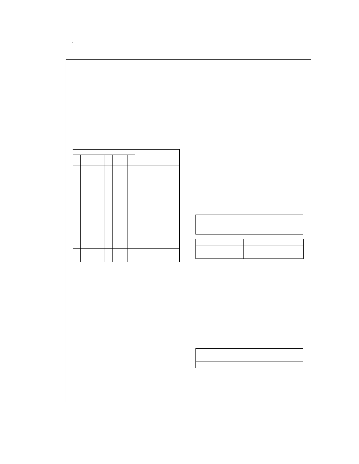
TABLE 2. Control Register Byte 2 Functions
Bit Number and Name
76 5 43210 Function
MA IA DN DL AL PP
F
1F0
0 0 MCLK=512 kHz
0 1 MCLK=1.536
1 0 MCLK=2.048 MHz
1 1 MCLK=4.096 MHz
0 X Select µ-255 law (Note 4)
1 0 A-law, Including Even
1 1 A-law, No Even Bit Inversion
0 Delayed Data Timing
1 Non-Delayed Data
0 0 Normal Operation
1 X Digital Loopback
0 1 Analog Loopback
Note 4: State at power-on initialization. (Bit 4=0)
or 1.544 MHz
(Note 4)
Bit Inversion
Timing (Note 4)
(Note 4)
0 Power Amp Enabled in PDN
1 Power Amp Disabled in
PDN (Note 4)
2.1 Master Clock Frequency Selection
A Master clock must be provided to COMBO II for operation
of the filter and coding/decoding functions. The MCLK frequency must be either 512 kHz, 1.536 MHz, 1.544 MHz,
2.048 MHz, or 4.096 MHz and must be synchronous with
BCLK. Bits F
ization to select the correct internal divider.
and F0(see
1
Table2
) must be set during initial-
2.2 Coding Law Selection
Bits “MA” and “IA” in
Table 2
permit the selection of µ255
coding or A-law coding, with or without even bit inversion.
2.3 Analog Loopback
Analog Loopback mode is entered by setting the “AL” and
“DL” bits in the Control Register as shown in
analog loopback mode, the Transmit input VF
from the input pin and internally connected to the VF
put, forming a loop from the Receive PCM Register back to
the Transmit PCM Register. The VF
and the programmed settings of the Transmit and Receive
O pin remains active,
R
Table 2
I is isolated
X
0 (and
X
.Inthe
O out-
R
gains remain unchanged, thus care must be taken to ensure
that overload levels are not exceeded anywhere in the loop.
Hybrid balance must be disabled for meaningful analog loopback function.
2.4 Digital Loopback
Digital Loopback mode is entered by setting the “AL” and
“DL” bits in the Control Register as shown in
Table 2
. This
mode provides another stage of path verification by enabling
data written into the Receive PCM Register to be read back
from that register in any Transmit time-slot at D
loopback, the decoder will remain functional and output a
signal at VF
be turned off by programming the receive gain register to all
O. If this is undesirable, the receive output can
R
0/1. In digital
X
zeros.
3.0 INTERFACE LATCH DIRECTIONS
Immediately following power-on, all Interface Latches assume they are inputs, and therefore all IL pins are in a high
impedance state. Each IL pin may be individually programmed as a logic input or output by writing the appropriate
instruction to the LDR, see
Table 1
and
Table 3
. For minimum power dissipation, unconnected latch pins should be
programmed as outputs. For the TP3071, L5 should always
be programmed as an output.
Bits L
the LDR with the L bits in the second byte set as follows:
must be set by writing the specified instruction to
5–L0
TABLE 3. Byte 2 Functions of Latch Direction Register
Byte 2 Bit Number
76543210
L
L1L2L3L4L5XX
0
LnBit IL Direction
0 Input
1 Output
X=don’t care
INTERFACE LATCH STATES
Interface Latches configured as outputs assume the state
determined by the appropriate data bit in the 2-byte instruction written to the Interface Latch Register (ILR) as shown in
Table1
and
Table4
. Latches configured as inputs will sense
the state applied by an external source, such as the
Off-Hook detect output of a SLIC. All bits of the ILR, i.e.
sensed inputs and the programmed state of outputs, can be
read back in the 2nd byte of a READ from the ILR.
It is recommended that during initialization, the state of IL
pins to be configured as outputs should be programmed first,
followed immediately by the Latch Direction Register.
TABLE 4. Interface Latch Data Bit Order
Bit Number
76543210
D
D1D2D3D4D5XX
0
www.national.com 6
Page 7
Programmable Functions (Continued)
TABLE 5. Coding Law Conventions
µ255 law
MSB LSB MSB LSB MSB LSB
=
V
+Full Scale 10000000 10101010 11111111
IN
=
V
0V 11111111 11010101 10000000
IN
01111111 01010101 00000000
=
V
−Full Scale 00000000 00101010 01111111
IN
Note 5: The MSB is always the first PCM bit shifted in or out of COMBO II.
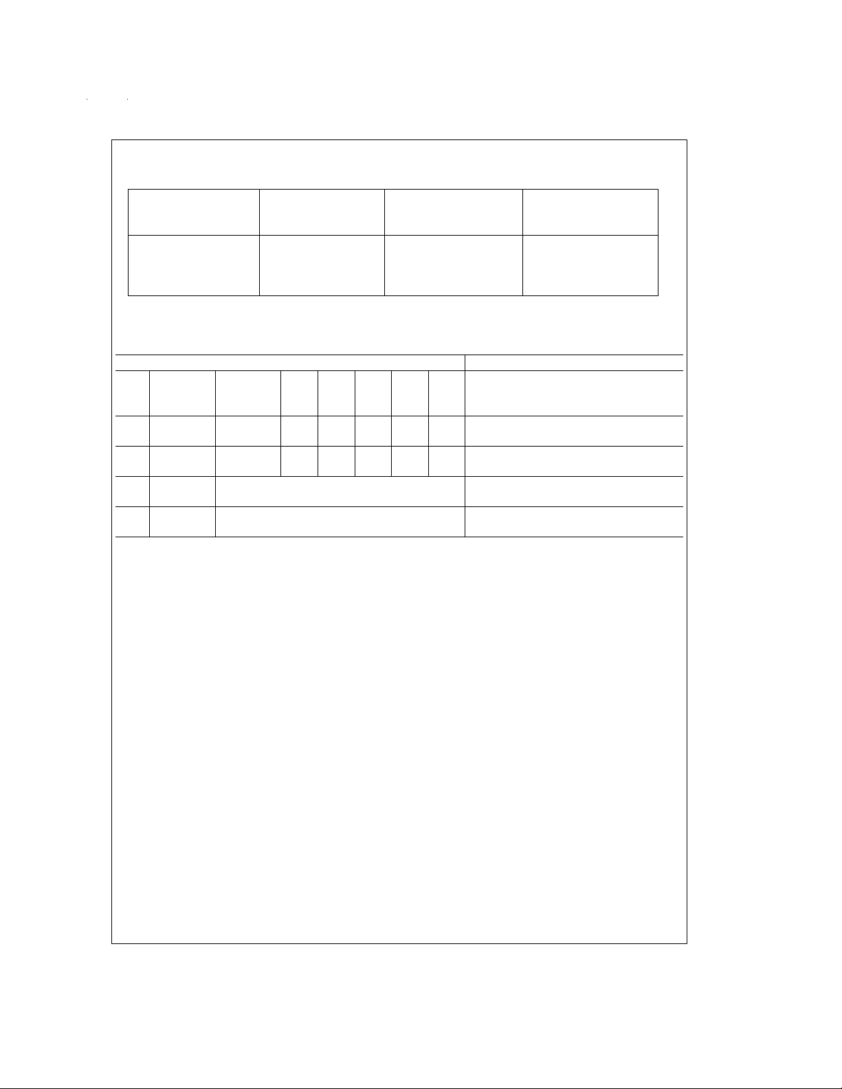
TABLE 6. Time-Slot and Port Assignment Instruction
Bit Number and Name Function
7 6 5 43210
EN PS T
5
T
T
4
T
3
2
(Note 6) (Note 7)
0 0 X XXXXXDisable D
0 1 X XXXXXDisable D
1 0 Assign One Binary Coded Time-Slot from 0–63 Enable D
Assign One Binary Coded Time-Slot from 0–63 Enable D
1 1 Assign One Binary Coded Time-Slot from 0–63 Enable D
Assign One Binary Coded Time-Slot from 0–63 Enable D
Note 6: The “PS” bit MUST always be set to 0 for the TP3071.
Note 7: T5 is the MSB of the Time-slot assignment bit field. Time slot bits should be set to “000000” for both transmit and receive when operating in non-delayed
data timing mode.
True A-law with A-law without
even bit inversion even bit inversion
T
T
1
0
0 Output (Transmit Instruction)
Disable D
Disable D
X
0 Input (Receive Instruction)
R
1 Output (Transmit Instruction)
X
1 Input (Receive Instruction)
R
0 Output (Transmit Instruction)
X
0 Input (Receive Instruction)
R
1 Output (Transmit Instruction)
X
1 Input (Receive Instruction)
R
5.0 TIME-SLOT ASSIGNMENT
COMBO II can operate in either fixed time-slot or time-slot
assignment mode for selecting the Transmit and Receive
PCM time-slots. Following power-on, the device is automatically in Non-Delayed Timing mode, in which the time-slot always begins with the leading (rising) edge of frame sync inputs FS
and FSR. Time-Slot Assignment may only be used
X
with Delayed Data timing; see
Figure 5
.FSXand FSRmay
have any phase relationship with each other in BCLK period
increments.
Alternatively, the internal time-slot assignment counters and
comparators can be used to access any time-slot in a frame,
using the frame sync inputs as marker pulses for the beginning of transmit and receive time-slot 0. In this mode, a
frame may consist of up to 64 time-slots of 8 bits each. A
time-slot is assigned by a 2-byte instruction as shown in
Table 1
and
Table 6
. The last 6 bits of the second byte indicate the selected time-slot from 0–63 using straight binary
notation. When writing a timeslot and port assignment register, if the PCM interface is currently active, it is immediately
deactivated to prevent possible bus clashes. A new assignment becomes active on the second frame following the end
of the Chip-Select for the second control byte. Rewriting of
register contents should not be performed during the talking
period of a connection to prevent waveform distortion
caused by loss of a sample which will occur with each register write. The “EN” bit allows the PCM inputs, D
puts, D
0/1, as appropriate, to be enabled or disabled.
X
0/1, or out-
R
Time-Slot Assignment mode requires that the FS
pulses must conform to the delayed data timing format
shown in
Figure 5
.
and FS
X
6.0 PORT SELECTION
On the TP3070 only, an additional capability is available; 2
Transmit serial PCM ports, D
rial PCM ports, D
two-way space switching to be implemented. Port selections
R
0 and DX1, and 2 Receive se-
X
0 and DR1, are provided to enable
for transmit and receive are made within the appropriate
time-slot assignment instruction using the “PS” bit in the second byte. The PS bit selects either Port 0 or Port 1. Both
ports cannot be active at the same time.
On the TP3071, only ports D
fore the “PS” bit MUST always be set to 0 for these devices.
Table 6
shows the format for the second byte of both trans-
0 and DR0 are available, there-
X
mit and receive time-slot and port assignment instructions.
7.0 TRANSMIT GAIN INSTRUCTION BYTE 2
The transmit gain can be programmed in 0.1 dB steps by
writing to the Transmit Gain Register as defined in
and
Table7
VF
+6.4 dBm to −19.0 dBm in 600Ω).
. This corresponds to a range of 0 dBm0 levels at
I between 1.619 Vrms and 0.087 Vrms (equivalent to
X
Table 1
To calculate the binary code for byte 2 of this instruction for
any desired input 0 dBm0 level in Vrms, take the nearest integer to the decimal number given by:
200 x log
(V/0.08595)
10
www.national.com7
R
Page 8

Programmable Functions (Continued)
and convert to the binary equivalent. Some examples are
given in
Table7
dix I of AN-614.
It should be noted that the Transmit (idle channel) Noise and
Transmit Signal to Total Distortion are both specified with
transmit gain set to 0 dB (Gain Register set to all ones). At
high transmit gains there will be some degradation in noise
performance for these parameters. See Application Note
AN-614 for more information on this subject.
TABLE 7. Byte 2 of Transmit Gain Instruction
Bit Number 0 dBm0 Test Level (Vrms)
76543210 atVF
00000000 NoOutput (Note 8)
00000001 0.087
00000010 0.088
11111110 1.600
11111111 1.619
Note 8: Analog signal path is cut off, but DXremains active and will output
codes representing idle noise.
8.0 RECEIVE GAIN INSTRUCTION BYTE 2
The receive gain can be programmed in 0.1 dB steps by writing to the Receive Gain Register as defined in
Table8
bility:
a) 0 dBm0 levels ≤ 1.96 Vrms at VF
a load of ≥ 15 kΩ to GND; receive gain set to 0 dB (Gain
Register set to all ones)
b) 0 dBm0 levels ≤ 1.85 Vrms at VF
a load of ≥ 600Ω to GND; receive gain set to −0.5 dB
c) 0 dBm0 levels ≤ 1.71 Vrms at VF
a load of ≥ 300Ω to GND; receive gain set to −1.2 dB
To calculate the binary code for byte 2 of this instruction for
any desired output 0 dBm0 level in Vrms, take the nearest integer to the decimal number given by:
and convert to the binary equivalent. Some examples are
given in
dix I of AN-614.
TABLE 8. Byte 2 of Receive Gain Instruction
Bit Number 0 dBm0 Test Level (Vrms)
76543210 atVF
00000000 NoOutput (Low Z to GND)
00000001 0.105
00000010 0.107
11111110 1.941
11111111 1.964
9.0 HYBRID BALANCE FILTER
The Hybrid Balance Filter on COMBO II is a programmable
filter consisting of a second-order section, Hybal1, followed
by a first-order section, Hybal2, and a programmable attenu-
www.national.com 8
and a complete tabulation is given in Appen-
I
X
——
Table 1
and
. Note the following restrictions on output drive capa-
O may be driven into
R
O may be driven into
R
O may be driven into
R
200 x log
Table8
and a complete tabulation is given in Appen-
(V/0.1043)
10
O
R
——
ator. Either of the filter sections can be bypassed if only one
is required to achieve good cancellation. A selectable 180
degree inverting stage is included to compensate for interface circuits which also invert the transmit input relative to
the receive output signal. The 2nd order section is intended
mainly to balance low frequency signals across a transformer SLIC, and the first order section to balance midrange
to higher audio frequency signals.
As a 2nd order section, Hybal1 has a pair of low frequency
zeroes and a pair of complex conjugate poles. When configuring Hybal1, matching the phase of the hybrid at low to
mid-band frequencies is most critical. Once the echo path is
correctly balanced in phase, the magnitude of the cancellation signal can be corrected by the programmable attenuator.
The 2nd order mode of Hybal1 is most suitable for balancing
interfaces with transformers having high inductance of 1.5
Henries or more. An alternative configuration for smaller
transformers is available by converting Hybal1 to a simple
first-order section with a single real low-frequency pole and
zero. In this mode, the pole/zero frequency may be programmed.
Many line interfaces can be adequately balanced by use of
the Hybal1 section only, in which case the Hybal2 filter
should be de-selected to bypass it.
Hybal2, the higher frequency first-order section, is provided
for balancing an electronic SLIC, and is also helpful with a
transformer SLIC in providing additional phase correction for
mid and high-band frequencies, typically 1 kHz to 3.4 kHz.
Such a correction is particularly useful if the test balance impedance includes a capacitor of 100 nF or less, such as the
loaded and non-loaded loop test networks in the United
States. Independent placement of the pole and zero location
is provided.
Figure 2
shows a simplified diagram of the local echo path
for a typical application with a transformer interface. The
magnitude and phase of the local echo signal, measured at
VF
I, are a function of the termination impedance ZT, the line
X
transformer and the impedance of the 2W loop, Z
pedance reflected back into the transformer primary is expressed as Z
VF
OtoVFXI is:
R
' then the echo path transfer function from
L
H(w)=Z
'/(ZT+ZL') (1)
L
. If the im-
L
9.1 PROGRAMMING THE FILTER
On initial power-up, the Hybrid Balance filter is disabled. Before the hybrid balance filter can be programmed it is necessary to design the transformer and termination impedance in
order to meet system 2W input return loss specifications,
which are normally measured against a fixed test impedance
(600 or 900Ω in most countries). Only then can the echo
path be modeled and the hybrid balance filter programmed.
Hybrid balancing is also measured against a fixed test impedance, specified by each national Telecom administration
to provide adequate control of talker and listener echo over
the majority of their network connections. This test impedance is Z
transhybrid loss obtained by the programmable filter must be
measured from the PCM digital input, D
tal output, D
conversion back to analog by a PCM CODEC/Filter.
in
Figure 2
L
X
. The echo signal and the degree of
0, to the PCM digi-
0, either by digital test signal analysis or by
R
Page 9
Programmable Functions (Continued)
FIGURE 2. Simplified Diagram of Hybrid Balance Circuit
Three registers must be programmed in COMBO II to fully
configure the Hybrid Balance Filter as follows:
Register 1: select/de-select Hybrid Balance Filter;
invert/non-invert cancellation signal;
select/de-select Hybal2 filter section;
attenuator setting.
Register 2: select/de-select Hybal1 filter;
set Hybal1 to 2nd order or 1st order;
pole and zero frequency selection.
Register 3: program pole frequency in Hybal2 filter;
program zero frequency in Hybal2 filter.
Standard filter design techniques may be used to model the
echo path (see
Equation (1)
) and design a matching hybrid
balance filter configuration. Alternatively, the frequency response of the echo path can be measured and the hybrid
balance filter designed to replicate it.
A Hybrid Balance filter design guide and software optimization program are available under license from National Semiconductor Corporation; order TP3077SW.
Applications Information
Figure 3
shows a typical application of the TP3071 together
with a typical monolithic SLIC. Four of the IL latches are configured as outputs to control the relay drivers on the SLIC,
while IL4 is an input for the Supervision signal.
DS008635-5
POWER SUPPLIES
While the pins of the TP3070 COMBO II devices are well
protected against electrical misuse, it is recommended that
the standard CMOS practice of applying GND to the device
before any other connections are made should always be
followed. In applications where the printed circuit card may
be plugged into a hot socket with power and clocks already
present, extra long pins on the connector should be used for
ground and V
nected between V
. In addition, a Schottky diode should be con-
BB
and ground.
BB
To minimize noise sources, all ground connections to each
device should meet at a common point as close as possible
to the device GND pin in order to prevent the interaction of
ground return currents flowing through a common bus impedance. Power supply decoupling capacitors of 0.1 µF
should be connected from this common device ground point
to V
and VBBas close to the device pins as possible. V
CC
and VBBshould also be decoupled with Low Effective Series
CC
Resistance Capacitors of at least 10 µF located near the
card edge connector.
Further guidelines on PCB layout techniques are provided in
Application NoteAN-614, “ COMBO II
™
Programmable PCM
CODEC/Filter Family Application Guide”.
www.national.com9
Page 10

Applications Information (Continued)
FIGURE 3. Typical Application with Monolithic SLIC
DS008635-7
www.national.com 10
Page 11
Absolute Maximum Ratings (Note 9)
If Military/Aerospace specified devices are required,
please contact the National Semiconductor Sales Office/
Distributors for availability and specifications.
V
to GND 7V
CC
Voltage at VF
Voltage at any Digital Input V
IV
X
+ 0.5V to VBB− 0.5V
CC
+ 0.5V to GND − 0.5V
CC
Storage Temperature Range −65˚C to + 150˚C
V
to GND −7V
BB
Current at VF
0
R
Current at any Digital Output
±
100 mA
±
50 mA
Lead Temperature
(Soldering, 10 sec.) 300˚C
Electrical Characteristics
=
Unless otherwise noted, limits printed in BOLD characters are guaranteed for V
+70˚C (−40˚C to +85˚C for TP3070-X) by correlation with 100%electrical testing at T
correlation with other production tests and/or product design and characterization. All signals referenced to GND. Typicals
specified at V
=
+5V, V
CC
=
BB
−5V, T
=
25˚C.
A
CC
±
+5V
=
25˚C. All other limits are assured by
A
Symbol Parameter Conditions Min Typ Max Units
DIGITAL INTERFACES
V
V
V
V
I
IL
I
IH
Input Low Voltage All Digital Inputs (DC Meas.) (Note 10) 0.7 V
IL
Input High Voltage All Digital Inputs (DC Meas.) (Note 10) 2.0 V
IH
Output Low Voltage DX0, DX1, TSX0, TSX1 and CO, I
OL
All Other Digital Outputs, I
Output High Voltage DX0, DX1 and CO, I
OH
All Other Digital Outputs (except TS
All Digital Outputs, I
Input Low Current Any Digital Input, GND<V
Input High Current Any Digital Input except MR, V
=
−3.2 mA, 2.4 V
L
=
−100 µA V
L
=
3.2 mA,
L
=
1mA
L
=
), I
−1 mA
X
L
<
V
IN
IL
<
<
V
IH
V
IN
CC
MR Only −10 100 µA
I
OZ
Output Current in DX0, DX1, TSX0, TSX1, CO and CI/O (as an Output)
High Impedance IL5–IL0 When Selected as Inputs −10 10 µA
<
State (TRI-STATE) GND
<
V
V
OUT
CC
−40˚C to +85˚C (TP3070-X) −30 30 µA
ANALOG INTERFACES
I
VFXI
R
VOS
RL
Input Current, VFXI −3.3V<VFXI<3.3V −10.0 10.0 µA
Input Resistance −3.3V<VFXI<3.3V 390 620 kΩ
VFXI
Input Offset Voltage Transmit Gain=0 dB 200 mV
X
Applied at VF
Load Resistance Receive Gain=0 dB 15k
VFRO
I Transmit Gain=25.4 dB 10 mV
X
Receive Gain=−0.5 dB 600 Ω
Receive Gain=−1.2 dB 300
CL
RO
VOS
Load Capacitance RL
VFRO
Output Resistance Steady Zero PCM Code Applied to 1.0 3.0 Ω
VFRO
Output Offset Alternating±Zero PCM Code Applied to −200 200 mV
R
Voltage at V
FRO
≥ 300Ω 200 pF
VFRO
CL
from VFROtoGND
VFRO
D
0orDR1
R
DR0orDR1, Maximum Receive Gain
POWER DISSIPATION
I
0 Power Down Current CCLK, CI/O, CI, CO,=0.4V, CS=2.4V
CC
Interface Latches Set as Outputs with No Load, 0.1 0.6 mA
All Other Inputs Active, Power Amp Disabled
I
0 Power Down Current As Above −0.1 −0.3 mA
BB
−40˚C to +85˚C (TP3070-X) −0.4 mA
I
1 Power Up Current CCLK, CI/O, CI, CO=0.4V, CS=2.4V
CC
No Load on Power Amp 8.0 11.0 mA
Interface Latches Set as Outputs with No Load
−40˚C to +85˚C (TP3070-X) 13.0 mA
=
5%,V
BB
− 0.5 V
CC
−5V
±
5%;T
−10 10 µA
−10 10 µA
=
0˚C to
A
0.4 V
www.national.com11
Page 12

Electrical Characteristics (Continued)
=
Unless otherwise noted, limits printed in BOLD characters are guaranteed for V
+70˚C (−40˚C to +85˚C for TP3070-X) by correlation with 100%electrical testing at T
correlation with other production tests and/or product design and characterization. All signals referenced to GND. Typicals
specified at V
=
+5V, V
CC
=
BB
−5V, T
=
25˚C.
A
CC
±
+5V
=
25˚C. All other limits are assured by
A
Symbol Parameter Conditions Min Typ Max Units
POWER DISSIPATION
I
1 Power Up Current As Above −8.0 −11.0 mA
BB
−40˚C to +85˚C (TP3070-X) −13.0 mA
I
2 Power Down Current Power Amp Enabled 2.0 3.0 mA
CC
−40˚C to +85˚C (TP3070-X) 4.0 mA
I
2 Power Down Current Power Amp Enabled −2.0 −3.0 mA
BB
−40˚C to +85˚C (TP3070-X) −4.0 mA
Note 9: “Absolute Maximum Ratings” indicate limits beyond which damage to the device may occur. Operating Ratings indicate conditions for which the device is
functional, but do not guarantee specific performance limits.
Note 10: See definitions and timing conventions section.
5%,V
=
±
−5V
BB
5%;T
=
0˚C to
A
Timing Specifications
=
Unless otherwise noted, limits printed in BOLD characters are guaranteed for V
+70˚C (−40˚C to +85˚C for TP3070-X) by correlation with 100%electrical testing at T
correlation with other production tests and/or product design and characterization. All signals referenced to GND. Typicals
specified at V
All timing parameters are measured at V
See Definitions and Timing Conventions section for test methods information.
=
+5V, V
CC
=
BB
−5V, T
A
=
OH
25˚C.
=
2.0V and V
=
0.7V.
OL
CC
±
+5V
=
25˚C. All other limits are assured by
A
Symbol Parameter Conditions Min Typ Max Units
MASTER CLOCK TIMING
f
MCLK
t
WMH
t
WML
t
RM
t
FM
t
HBM
Frequency of MCLK Selection of Frequency is 512 kHz
Programmable (See
Table 5
) 1536 kHz
Period of MCLK High Measured from VIHto VIH(Note 11) 80 ns
Period of MCLK Low Measured from VILto VIL(Note 11) 80 ns
Rise Time of MCLK Measured from VILto V
Fall Time of MCLK Measured from VIHto V
IH
IL
HOLD Time, BCLK LOW TP3070 Only 50 ns
to MCLK HIGH
t
WFL
Period of FSXor FSRLow Measured from VILto V
IL
1 MCLK Period
PCM INTERFACE TIMING
f
BCLK
Frequency of BCLK May Vary from 64 kHz to 4096 kHz 64 4096 kHz
in 8 kHz Increments
t
t
t
t
t
t
WBH
WBL
RB
FB
HBF
SFB
Period of BCLK High Measured from VIHto V
Period of BCLK Low Measured from VILto V
Rise Time of BCLK Measured from VILto V
Fall Time of BCLK Measured from VIHto V
IH
IL
IH
IL
80 ns
80 ns
Hold Time, BCLK Low 30 ns
to FS
High or Low
X/R
Setup Time, FS
X/R
30 ns
High to BCLK Low
t
DBD
Delay Time, BCLK High Load=100 pF Plus 2 LSTTL Loads 80 ns
to Data Valid −40˚C to +85˚C (TP3070-X) 90 ns
=
5%;V
BB
−5V
±
5%;T
1544 kHz
2048 kHz
4096 kHz
30 ns
30 ns
30 ns
30 ns
=
0˚C to
A
www.national.com 12
Page 13

Timing Specifications (Continued)
=
Unless otherwise noted, limits printed in BOLD characters are guaranteed for V
+70˚C (−40˚C to +85˚C for TP3070-X) by correlation with 100%electrical testing at T
correlation with other production tests and/or product design and characterization. All signals referenced to GND. Typicals
specified at V
All timing parameters are measured at V
See Definitions and Timing Conventions section for test methods information.
=
+5V, V
CC
=
BB
−5V, T
A
=
OH
25˚C.
=
2.0V and V
=
0.7V.
OL
CC
±
+5V
=
25˚C. All other limits are assured by
A
Symbol Parameter Conditions Min Typ Max Units
PCM INTERFACE TIMING
t
DBZ
t
DBT
t
ZBT
t
DFD
Delay Time, BCLK Low to DX0/1 DX0/1 Disabled is measured at V
Disabled if FSXLow, FSXLow to
D
0/1 disabled if 8th BCLK 15 80 ns
X
Low, or BCLK High to D
Disabled if FS
X
0/1
X
High −40˚C to +85˚C (TP3070-X) 15 100 ns
Delay Time, BCLK High to TS
Low if FSXHigh, or FSXHigh to
Low if BCLK High (Non
TS
X
Delayed Mode); BCLK High to
Low (Delayed Data Mode)
TS
X
or VOHaccording to
Figure 5
Load=100 pF Plus 2 LSTTL Loads 60 ns
X
Figure 4
TRI-STATE Time, BCLK Low to
High if FSXLow, FSXLow
TS
X
to TSXHigh if 8th BCLK Low, or
BCLK High to TSXHigh if FS
High
Delay Time, FS
X/R
High to Data Valid Applies if FS
X
Load=100 pF Plus 2 LSTTL Loads,
Rises Later than 80 ns
X/R
OL
or
15 60 ns
BCLK Rising Edge in Non-Delayed
Data Mode Only
−40˚C to +85˚C (TP3070-X) 90 ns
t
SDB
Setup Time, DR0/1 30 ns
Valid to BCLK Low
t
HBD
Hold Time, BCLK 15 ns
Low to D
0/1 Invalid −40˚C to +85˚C (TP3070-X) 15 ns
R
SERIAL CONTROL PORT TIMING
f
CCLK
t
WCH
t
WCL
t
RC
t
FC
t
HCS
Frequency of CCLK 2048 kHz
Period of CCLK High Measured from VIHto V
Period of CCLK Low Measured from VILto V
Rise Time of CCLK Measured from VILto V
Fall Time of CCLK Measured from VIHto V
IH
IL
IH
IL
160 ns
160 ns
Hold Time, CCLK Low CCLK1 10 ns
to CS Low
t
HSC
Hold Time, CCLK CCLK 8 100 ns
Low to CS High
t
SSC
Setup Time, CS 60 ns
Transition to CCLK Low
t
SSCO
Setup Time, CS 50 ns
Transition to CCLK High
t
SDC
Setup Time, CI (CI/O) 50 ns
Data In to CCLK Low
t
HCD
Hold Time, CCLK 50 ns
Low to CI/O Invalid
t
DCD
Delay Time, CCLK High Load=100 pF plus 2 LSTTL Loads 80 ns
to CI/O Data Out Valid −40˚C to +85˚C (TP3070-X) 100 ns
5%;V
=
±
−5V
BB
5%;T
=
0˚C to
A
50 ns
50 ns
www.national.com13
Page 14

Timing Specifications (Continued)
=
Unless otherwise noted, limits printed in BOLD characters are guaranteed for V
+70˚C (−40˚C to +85˚C for TP3070-X) by correlation with 100%electrical testing at T
correlation with other production tests and/or product design and characterization. All signals referenced to GND. Typicals
specified at V
All timing parameters are measured at V
See Definitions and Timing Conventions section for test methods information.
=
+5V, V
CC
=
BB
−5V, T
A
=
OH
25˚C.
=
2.0V and V
=
0.7V.
OL
CC
±
+5V
=
25˚C. All other limits are assured by
A
Symbol Parameter Conditions Min Typ Max Units
SERIAL CONTROL PORT TIMING
t
DSD
Delay Time, CS Low Applies Only if Separate 80 ns
to CO (CI/O) Valid CS used for Byte 2
−40˚C to +85˚C (TP3070-X) 100 ns
t
DDZ
5%;V
=
−5V
BB
±
5%;T
=
0˚C to
A
Page 15

Timing Diagrams (Continued)
DS008635-9
FIGURE 5. Delayed Data Timing Mode
(Time Slot Zero Only)
www.national.com15
Page 16
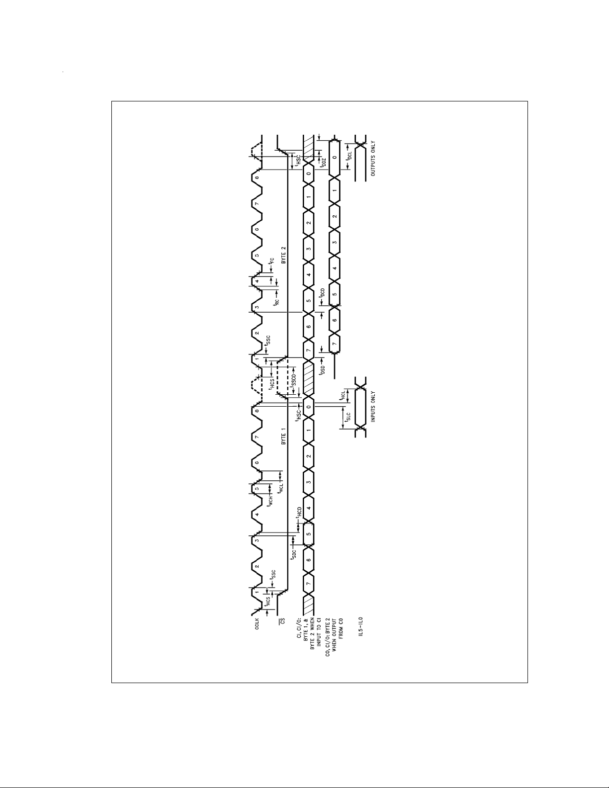
Timing Diagrams (Continued)
DS008635-10
www.national.com 16
FIGURE 6. Control Port Timing
Page 17

Transmission Characteristics
Page 18

Transmission Characteristics (Continued)
Page 19
Transmission Characteristics (Continued)
=
Unless otherwise noted, limits printed in BOLD characters are guaranteed for V
+70˚C (−40˚C to +85˚C for TP3070-X) by correlation with 100%electrical testing at T
0 dBm0, D
gain), hybrid balance filter disabled. All other limits are assured by correlation with other production tests and/or product design and characterization. All signals referenced to GND. Typicals specified at V
0orDR1=0 dBm0 PCM code. Transmit and receive gains programmed for maximum 0 dBm0 test levels (0 dB
R
CC
CC
±
+5V
=
25˚C. f=1015.625 Hz, VF
A
=
+5V, V
Symbol Parameter Conditions Min Typ Max Units
AMPLITUDE RESPONSE
G
Receive Gain Sinusoidal Test Method.
RAL
Variation with Signal Reference Level=0 dBm0.
Level D
0=−40 dBm0 to +3 dBm0 −0.2 0.2 dB
R
D
0=−50 dBm0 to −40 dBm0 −0.4 0.4 dB
R
D
0=−55 dBm0 to − 50 dBm0 −1.2 1.2 dB
R
D
0=3.1 dBm0
R
R
R
=
L
=
L
600Ω,G
300Ω,G
=
−0.5 dB −0.2 0.2 dB
R
=
−1.2 dB −0.2 0.2 dB
R
ENVELOPE DELAY DISTORTION WITH FREQUENCY
D
D
Tx Delay, Absolute f=1600 Hz 315 µs
XA
Tx Delay, Relative to D
XR
XA
f=500–600 Hz 220 µs
f=600–800 Hz 145 µs
f=800–1000 Hz 75 µs
f=1000–1600 Hz 40 µs
f=1600–2600 Hz 75 µs
f=2600–2800 Hz 105 µs
f=2800–3000 Hz 155 µs
D
D
Rx Delay, Absolute f=1600 Hz 200 µs
RA
Rx Delay, Relative to D
RR
f=500–1000 Hz −40 µs
RA
f=1000–1600 Hz −30 µs
f=1600–2600 Hz 90 µs
f=2600–2800 Hz 125 µs
f=2800–3000 Hz 175 µs
NOISE
N
Transmit Noise, C Message (Note 12) 12 15 dBrnC0
XC
Weighted, µ-law Selected All ‘1’s in Gain Register
N
Transmit Noise, P Message (Note 12) −74 −67 dBm0p
XP
Weighted, A-law Selected All ‘1’s in Gain Register
N
Receive Noise, C Message PCM Code is Alternating Positive 8 11 dBrnC0
RC
Weighted, µ-law Selected and Negative Zero
N
Receive Noise, P Message PCM Code Equals Positive Zero −82 −79 dBm0p
RP
Weighted, A-law Selected
N
PPSR
Noise, Single Frequency f=0 kHz to 100 kHz, Loop Around −53 dBm0
RS
Positive Power Supply V
X
Measurement, VF
=
5.0 V
CC
DC
I=0 Vrms
X
+ 100 mVrms
Rejection, Transmit f=0 kHz–4 kHz (Note 13) 36 dBC
f=4 kHz–50 kHz 30 dBC
NPSR
Negative Power Supply V
X
=
−5.0 V
BB
+ 100 mVrms
DC
Rejection, Transmit f=0 kHz–4 kHz (Note 13) 36 dBC
f=4 kHz–50 kHz 30 dBC
5%,V
=
BB
=
BB
−5V, T
−5V
=
±
5%;T
=
25˚C.
A
0˚C to
A
=
I
X
www.national.com19
Page 20
Transmission Characteristics (Continued)
=
Unless otherwise noted, limits printed in BOLD characters are guaranteed for V
+70˚C (−40˚C to +85˚C for TP3070-X) by correlation with 100%electrical testing at T
0 dBm0, D
gain), hybrid balance filter disabled. All other limits are assured by correlation with other production tests and/or product design and characterization. All signals referenced to GND. Typicals specified at V
0orDR1=0 dBm0 PCM code. Transmit and receive gains programmed for maximum 0 dBm0 test levels (0 dB
R
CC
CC
±
+5V
=
25˚C. f=1015.625 Hz, VF
A
=
+5V, V
Symbol Parameter Conditions Min Typ Max Units
NOISE
PPSR
Positive Power Supply PCM Code Equals Positive Zero
R
Rejection, Receive V
=
5.0 V
CC
Measure VF
+ 100 mVrms
DC
O
R
f=0 Hz–4000 Hz 36 dBC
f=4 kHz–25 kHz 40 dB
f=25 kHz–50 kHz 36 dB
NPSR
Negative Power Supply PCM Code Equals Positive Zero
R
Rejection, Receive V
=
−5.0 V
BB
Measure VF
+ 100 mVrms
DC
O
R
f=0 Hz–4000 Hz 36 dBC
f=4 kHz–25kHz 40 dB
f=25 kHz–50 kHz 36 dB
SOS Spurious Out-of-Band 0 dBm0, 300 Hz to 3400 Hz Input PCM
Signals at the Channel Code Applied at D
0 (or DR1)
R
Output 4600 Hz–7600 Hz −30 dB
7600 Hz–8400 Hz −40 dB
8400 Hz–50,000 Hz −30 dB
DISTORTION
STD
STD
Signal to Total Distortion Sinusoidal Test Method
X
Transmit or Receive Level=3.0 dBm0 33 dBC
R
Half-Channel, µ-law Selected=0 dBm0 to − 30 dBm0 36 dBC
=
−40 dBm0 30 dBC
=
−45 dBm0 25 dBC
STD
Signal to Total Distortion Sinusoidal Test Method
RL
Receive with Level=+3.1 dBm0
SFD
R
=
L
=
L
600Ω,G
300Ω,G
Resistive Load R
Single Frequency −46 dB
X
=
−0.5 dB 33 dBC
R
=
−1.2 dB 33 dBC
R
Distortion, Transmit
SFD
Single Frequency −46 dB
R
Distortion, Receive
IMD Intermodulation Distortion Transmit or Receive
Two Frequencies in the Range −41 dB
300 Hz–3400 Hz
5%,V
=
BB
=
BB
−5V, T
−5V
=
±
5%;T
=
25˚C.
A
0˚C to
A
=
I
X
www.national.com 20
Page 21
Transmission Characteristics (Continued)
Page 22

Definitions and Timing Conventions
DEFINITIONS
V
IH
V
IL
V
OH
V
OL
Threshold Region The threshold region is the range of in-
Valid Signal A signal is Valid if it is in one of the valid
Invalid signal A signal is invalid if it is not in a valid
TIMING CONVENTIONS
For the purposes of this timing specification the following
conventions apply.
Input Signals All input signals may be characterized
Period The period of the clock signal is desig-
Rise Time Rise times are designated as t
Fall Time Fall times are designated as t
Pulse Width High The high pulse width width is designated
VIHis the D.C. input level above which
an input level is guaranteed to appear as
a logical one. This parameter is to be
measured by performing a functional
test at reduced clock speeds and nominal timing, (i.e., not minimum setup and
hold times or output strobes), with the
high level of all driving signals set to V
and maximum supply voltages applied
to the device.
VILis the D.C. input level below which
an input level is guaranteed to appear as
a logical zero to the device. This parameter is measured in the same manner as
V
but with all driving signal low levels
IH
set to V
applied to the device.
and minimum supply voltages
IL
VOHis the minimum D.C. output level to
which an output placed in a logical one
state will converge when loaded at the
maximum specified load current.
VOLis the maximum D.C. output level to
which an output placed in a logical zero
state will converge when loaded at the
maximum specified load current.
put voltages between V
logic states. (i.e., above V
V
). In timing specifications, a signal is
IL
deemed valid at the instant it enters a
and VIH.
IL
or below
IH
valid state.
logic state, i.e., when it is in the threshold region between V
specifications, a signal is deemed In-
and VIH. In timing
IL
valid at the instant it enters the threshold
region.
=
as: V
L
10 ns.
nated as t
mnemonic of the clock signal being
=
0.4V,V
2.4V,t
H
wherexxrepresents the
Pxx
R
<
10 ns, t
F
specified.
, where
yy represents a mnemonic of the signal
whose rise time is being specified. t
measured from V
IL
to VIH.
yy represents a mnemonic of the signal
whose fall time is being specified. t
measured from V
as t
, where zz represents the mne-
WzzH
monic of the input or output signal whose
IH
to VIL.
Ryy
Fyy
Ryy
, where
Fyy
pulse width is being specified. High
IH
<
is
is
pulse widths are measured from V
V
.
IH
IH
Pulse Width Low The low pulse width is designated as
t
, where zz represents the mne-
WzzL
monic of the input or output signal whose
pulse width is being specified. Low pulse
widths are measured from V
Setup Time Setup times are designated as t
where ww represents the mnemonic of
IL
to VIL.
Swwxx
the input signal whose setup time is being specified relative to a clock or strobe
input represented by mnemonic xx.
Setup times are measured from the ww
Valid to xx Invalid.
Hold Time Hold times are designated as T
where ww represents the mnemonic of
Hwwxx
the input signal whose hold time is being
specified relative to a clock or strobe input represented by the mnemonic xx.
Hold times are measured from xx Valid
to ww Invalid.
Delay Time Delay times are designated as
T
[ IHIL], where xx represents the
Dxxyy
mnemonic of the input reference signal
and yy represents the mnemonic of the
output signal whose timing is being
specified relative to xx. The mnemonic
may optionally be terminated by an H or
L to specify the high going or low going
transition of the output signal. Maximum
delay times are measured from xx Valid
to yy Valid. Minimum delay times are
measured from xx Valid to yy Invalid.
This parameter is tested under the load
conditions specified in the Conditions
column of the Timing Specifications section of this datasheet.
to
,
,
www.national.com 22
Page 23

23
Page 24
Physical Dimensions inches (millimeters) unless otherwise noted
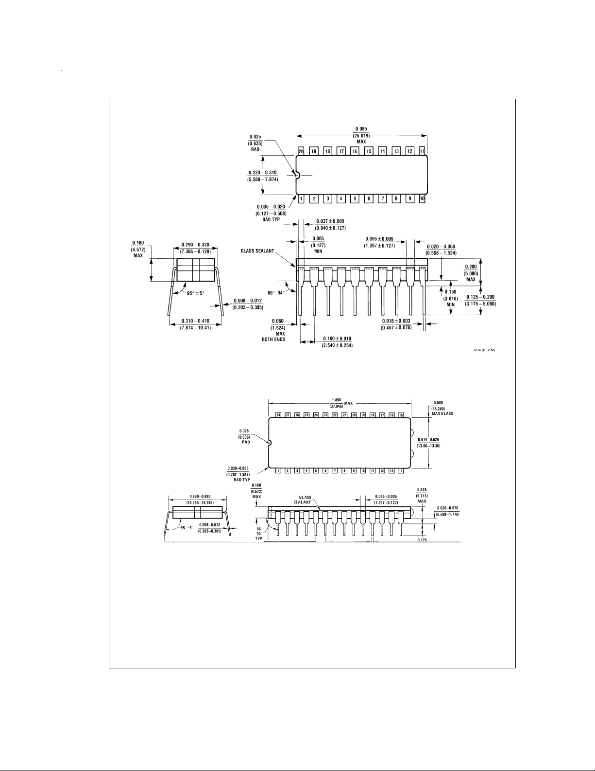
Ceramic Dual-In-Line Package (J)
Order Number TP3071J
NS Package Number J20A
Ceramic Dual-In-Line Package (J)
Order Number TP3070J
NS Package Number J28A
www.national.com 24
Page 25
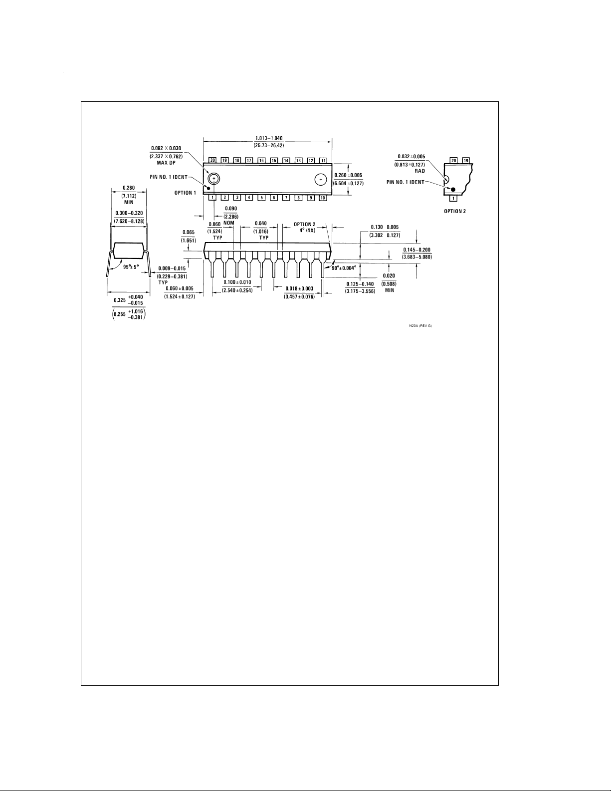
Physical Dimensions inches (millimeters) unless otherwise noted (Continued)
Molded Dual-In-Line Package (N)
Order Number TP3071N
NS Package Number N20A
www.national.com25
Page 26

Physical Dimensions inches (millimeters) unless otherwise noted (Continued)
Plastic Leaded Chip Carrier (V)
Order Number TP3070V or TP3070V-X
NS Package Number V28A
LIFE SUPPORT POLICY
TP3070, TP3071, TP3070-X COMBO II Programmable PCM CODEC/Filter
NATIONAL’S PRODUCTS ARE NOT AUTHORIZED FOR USE AS CRITICAL COMPONENTS IN LIFE SUPPORT DEVICES OR SYSTEMS WITHOUT THE EXPRESS WRITTEN APPROVAL OF THE PRESIDENT OF NATIONAL SEMICONDUCTOR CORPORATION. As used herein:
1. Life support devices or systems are devices or systems which, (a) are intended for surgical implant into
the body, or (b) support or sustain life, and whose failure to perform when properly used in accordance
2. A critical component is any component of a life support
device or system whose failure to perform can be reasonably expected to cause the failure of the life support
device or system, or to affect its safety or effectiveness.
with instructions for use provided in the labeling, can
be reasonably expected to result in a significant injury
to the user.
National Semiconductor
Corporation
Americas
Tel: 1-800-272-9959
Fax: 1-800-737-7018
Email: support@nsc.com
www.national.com
National does not assume any responsibility for use of any circuitry described, no circuit patent licenses are implied and National reserves the right at any time without notice to change said circuitry and specifications.
National Semiconductor
Europe
Fax: +49 (0) 1 80-530 85 86
Email: europe.support@nsc.com
Deutsch Tel: +49 (0) 1 80-530 85 85
English Tel: +49 (0) 1 80-532 78 32
Français Tel: +49 (0) 1 80-532 93 58
Italiano Tel: +49 (0) 1 80-534 16 80
National Semiconductor
Asia Pacific Customer
Response Group
Tel: 65-2544466
Fax: 65-2504466
Email: sea.support@nsc.com
National Semiconductor
Japan Ltd.
Tel: 81-3-5639-7560
Fax: 81-3-5639-7507
 Loading...