NATIONAL SEMICONDUCTOR TP3040V, TP3040N, TP3040AN Datasheet

TP3040, TP3040A PCM Monolithic Filter
TP3040, TP3040A PCM Monolithic Filter
September 1994
General Description
The TP3040/TP3040A filter is a monolithic circuit containing both transmit and receive filters specifically designed for
PCM CODEC filtering applications in 8 kHz sampled systems.
The filter is manufactured using microCMOS technology
and switched capacitor integrators are used to simulate
classical LC ladder filters which exhibit low component sensitivity.
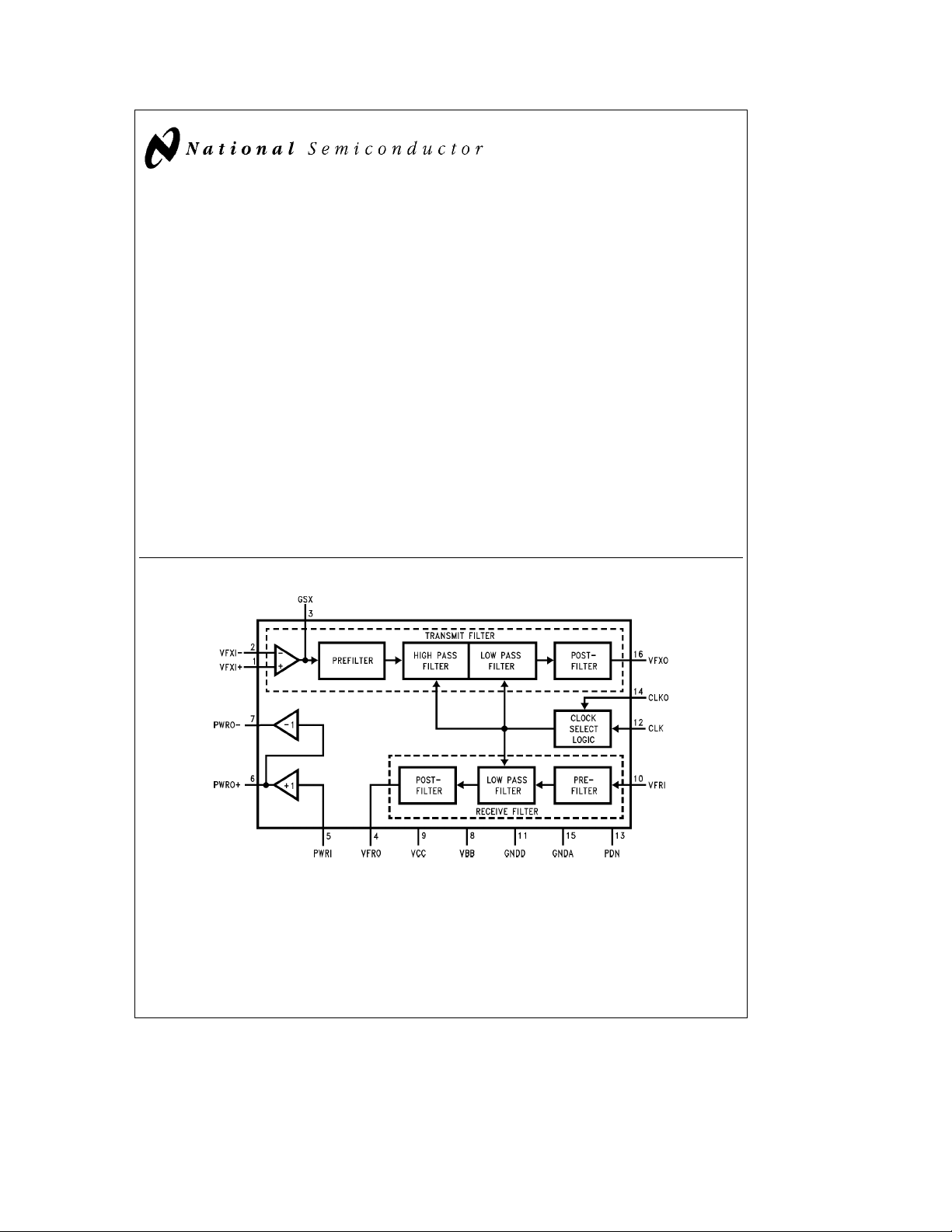
TRANSMIT FILTER STAGE
The transmit filter is a fifth order elliptic low pass filter in
series with a fourth order Chebyshev high pass filter. It provides a flat response in the passband and rejection of signals below 200 Hz and above 3.4 kHz.
RECEIVE FILTER STAGE
The receive filter is a fifth order elliptic low pass filter designed to reconstruct the voice signal from the decoded/demultiplexed signal which, as a result of the sampling process, is a stair-step signal having the inherent sin x/x frequency response. The receive filter approximates the function required to compensate for the degraded frequency response and restore the flat passband response.
Block Diagram
Features
Y
Designed for D3/D4 and CCITT applications
Y
a
5V,b5V power supplies
Y
Low power consumption:
45 mW (0 dBm0 into 600X)
30 mW (power amps disabled)
Y
Power down mode: 0.5 mW
Y
20 dB gain adjust range
Y
No external anti-aliasing components
Y
Sin x/x correction in receive filter
Y
50/60 Hz rejection in transmit filter
Y
TTL and CMOS compatible logic
Y
All inputs protected against static discharge due to
handling
FIGURE 1
TL/H/6660– 1
C
1995 National Semiconductor Corporation RRD-B30M115/Printed in U. S. A.
TL/H/6660

Absolute Maximum Ratings
If Military/Aerospace specified devices are required,
please contact the National Semiconductor Sales
Office/Distributors for availability and specifications.
Supply Voltages
g
7V
Power Dissipation 1 W/Package
Input Voltage
Voltage at Any Input
or Output V
DC Electrical Characteristics Unless otherwise noted, limits printed in BOLD characters are guaranteed for
ea
V
limits are assured by correlation with other production tests and/or product design and characterization. Typicals specified at
V
digital ground, GNDD. Analog voltages measured with respect to analog ground, GNDA.
CC
CC
5.0Vg5%, V
ea
5.0V, V
BB
BB
eb
5.0V, T
eb
5.0Vg5%; T
a
0.3V to V
CC
A
e
25§C. Clock frequency is 2.048 MHz. Digital interface voltages measured with respect to
A
g
7V
b
0.3V
BBV
e
0§Cto70§C by correlation with 100% electrical testing at T
Symbol Parameter Conditions Min Typ Max Units
POWER DISSIPATION
I
CC0
VCCStandby Current V
e
CC
CLK0 and PWRI
All other pins at GND (0V)
TP3040, TP3040A
I
BB0
VBBStandby Current V
e
CC
CLK0 and PWRI
All other pins at GND (0V)
TP3040, TP3040A
I
I
I
I
CC1
BB1
CC2
BB2
VCCOperating Current PWRIeVBB, Power Amp Inactive 3.0 4.0 mA
VBBOperating Current PWRIeVBB, Power Amp Inactive 3.0 4.0 mA
VCCOperating Current (Note 1) 4.6 6.4 mA
VBBOperating Current (Note 1) 4.6 6.4 mA
DIGITAL INTERFACE
I
I
I
V
V
V
V
V
INC
INP
IN0
IL
IH
IL0
II0
IH0
Input Current, CLK V
Input Current, PDN V
Input Current, CLK0 V
Input Low Voltage, CLK, PDN 0 0.8 V
Input High Voltage, CLK, PDN 2.2 V
Input Low Voltage, CLK0 V
Input Intermediate Voltage, CLK0
Input High Voltage, CLK0 V
BB
BB
BB
s
s
s
TRANSMIT INPUT OP AMP
IBxI Input Leakage Current, VFxI
RIxI Input Resistance, VFxIV
VOSxI Input Offset Voltage, VFxI
V
CM
Common-Mode Range, VFxI
CMRR Common-Mode Rejection Ratio
PSRR Power Supply Rejection of VCCor V
R
OL
R
L
C
L
VOxI Output Voltage Swing, GS
A
VOL
F
c
Open Loop Output Resistance, GS
Minimum Load Resistance, GS
x
Maximum Load Capacitance, GS
x
Open Loop Voltage Gain, GS
x
Open Loop Unity Gain Bandwidth, GS
b
3.2VsV
s
BB
b
2.5VsV
b
2.5VsV
BB
x
x
t
R
10k
L
t
R
10k 5,000 V/V
L
x
Output Short-Circuit Duration Continuous
Operating Temperature Range
Storage Temperature
Lead Temperature (Soldering, 10 seconds) 300§C
ESD Rating to be determined
5.25V, V
5.25V, V
V
IN
V
IN
V
IN
VFxIsV
eb
5.25V,
BB
eb
5.25V (Note 6)
eb
5.25V,
BB
eb
5.25V (Note 6)
s
V
CC
s
V
CC
s
b
V
0.5V
CC
s
a
3.2V
IN
CC
s
a
2.5V
IN
s
2.5V 60 dB
IN
b
b
100 mA
b
b
CC
b
100 100 nA
10 MX
b
b
50 100 mA
50 100 mA
10 10 mA
10
BB
0.8 0.8 V
b
0.5 V
20 20 mV
2.5 2.5 V
60 dB
1kX
10 kX
g
2.5 V
2 MHz
b
25§Ctoa125§C
b
65§Ctoa150§C
e
25§C. All other
A
b
0.1 mA
CC
a
V
0.5 V
BB
CC
100 pF
V
V
2

AC Electrical Characteristics
Unless otherwise specified, T
assumed to be 1.54 Vrms measured at the output of the transmit or receive filter. Limits printed in BOLD characters are
guaranteed for V
25§C. All other limits are assured by correlation with other production tests and/or product design and characterization. Typicals
specified at V
CC
ea
CC
ea
Symbol Parameter Conditions Min Typ Max Units
TRANSMIT FILTER (Transmit filter input op amp set to the non-inverting unity gain mode, with VFxIe1.09 Vrms unless
otherwise noted.)
RL
CL
RO
Minimum Load Resistance, VFxO
x
Load Capacitance, VFxO 100 pF
x
Output Resistance, VFxO13X
x
PSRR1 VCCPower Supply Rejection, VFxOfe1 kHz, VFxIae0 Vrms 30 dB
PSRR2 VBBPower Supply Rejection, VFxO Same as Above 35 dB
GA
GR
DA
DD
Absolute Gain fe1 kHz (TP3040A) 2.9 3.0 3.1 dB
x
Gain Relative to GA
x
Absolute Delay at 1 kHz 250 ms
x
Differential Envelope Delay from 60 ms
x
1 kHz to 2.6 kHz
DPx1 Single Frequency Distortion
Products
DPx2 Distortion at Maximum Signal 0.16 Vrms, 1 kHz Signal Applied to
Level VF
NCx1 Total C Message Noise at VFxO TP3040, TP3040A 2 5 dBrnc0
NCx2 Total C Message Noise at VFxO Gain Setting Op Amp at 20 dB,
GAxT Temperature Coefficient of 0.0004 dB/§C
1 kHz Gain
GAxS Supply Voltage Coefficient of V
1 kHz Gain V
CT
Crosstalk, Receive to Transmit Receive Filter Outpute2.2 Vrms
RX
20 log
VF
x
VFRO
O
GRxL Gaintracking Relative to GA
e
A
5.0Vg5%, V
5.0V, V
BB
x
25§C. All parameters are specified for a signal level of 0 dBm0 at 1 kHz. The 0 dBm0 level is
eb
eb
BB
5.0V, T
x
5.0Vg5%; T
e
25§C.
A
b
2.5VkV
b
3.2VkV
e
f
Below 50 Hz
50 Hz
60 Hz
200 Hz (TP3040A)
200 Hz (TP3040)
300 Hz to 3 kHz (TP3040A)
300 Hz to 3 kHz (TP3040)
3.3 kHz
3.4 kHz
4.0 kHz
4.6 kHz and Above
Non-Inverting (Note 3)
T
A
TP3040, TP3040A
CC
BB
VF
Measure VF
Output Levelea3 dBm0
a
2 dBm0 tob40 dBm0
b
40 dBm0 tob55 dBm0
e
0§Cto70§C by correlation with 100% electrical testing at T
A
k
2.5V 3 kX
OUT
k
3.2V 10 kX
OUT
A
1 kHz (TP3040) 2.875 3.0 3.125 dB
b
b
41
b
b
1.5 0 dB
b
1.5 0.05 dB
b
0.125 0.125 dB
b
0.15 0.15 dB
b
0.35 0.03 dB
b
0.70
Ia, Gaine20 dB, R
x
e
0§Cto70§C
e
5.0Vg5% 0.01 dB/V
eb
5.0Vg5%
Iae0 Vrms, fe0.2 kHz to 3.4 kHz
x
O
x
e
10k
L
b
0.1 0.1 dB
b
0.05 0.05 dB
b
0.1 0.1 dB
35
b
15
3 6 dBrnc0
35 dB
b
35 dB
b
30 dB
b
0.1 dB
b
14 dB
b
32 dB
b
48 dB
b
45 dB
b
70 dB
e
3
 Loading...