

查询NM93C06LZ供应商
NM93C06LZ/C46LZ/C56LZ/C66LZ
256-/1024-/2048-/4096-Bit Serial EEPROM with Zero
Power and Extended Voltage (2.7V to 5.5V)
(MICROWIRE
TM
Bus Interface)
September 1996
NM93C06LZ/C46LZ/C56LZ/C66LZ 256-/1024-/2048-/4096-Bit Serial EEPROM with Zero Power
and Extended Voltage (2.7V to 5.5V) (MICROWIRE Bus Interface)
General Description
The NM93C06LZ/C46LZ/C56LZ/C66LZ devices are 256/
1024/2048/4096 bits respectively, of CMOS non-volatile
electrically erasable memory divided into 16/64/128/256
16-bit registers. They are fabricated using National Semiconductor’s floating-gate CMOS process for high reliability
and low power consumption. These memory devices are
available in both SO and TSSOP packages for small space
considerations.
The serial interface that operates these EEPROMs is MICROWIRE compatible for simple interface to standard microcontrollers and microprocessors. There are 7 instructions that control these devices: Read, Erase/Write Enable,
Erase, Erase All, Write, Write All, and Erase/Write Disable.
The ready/busy status is available on the DO pin to indicate
the completion of a programming cycle.
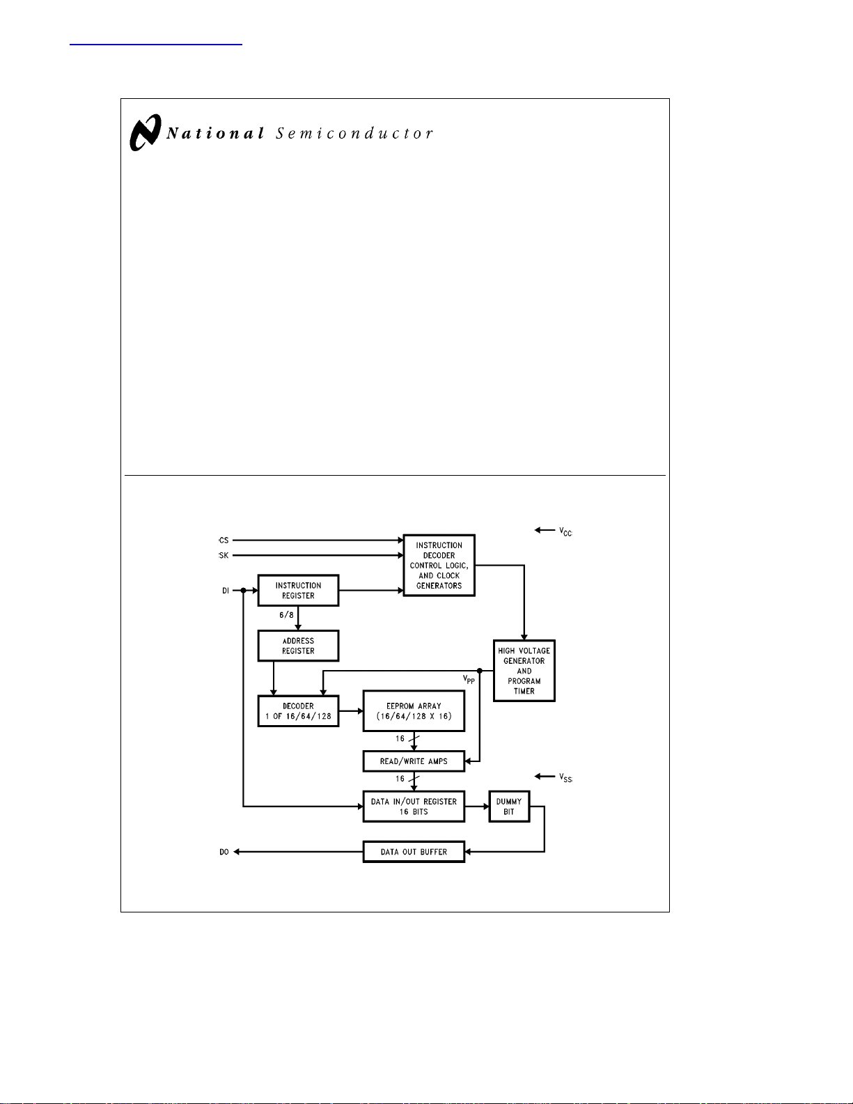
Block Diagram
Features
Y
Less than 1.0 mA standby current
Y
2.7V–5.5V operation in all modes
Y
Typical active current of 100 mA
Y
Direct write: no erase before program
Y
Reliable CMOS floating gate technology
Y
MICROWIRE compatible serial I/O
Y
Self-timed programming cycle
Y
Device status indication during programming mode
Y
40 years data retention
Y
Endurance: 106data changes
Y
Packages available: 8-pin SO, 8-pin DIP, 8-pin TSSOP
TRI-STATEÉis a registered trademark of National Semiconductor Corporation.
TM
MICROWIRE
C
1996 National Semiconductor Corporation RRD-B30M96/Printed in U. S. A.
is a trademark of National Semiconductor Corporation.
TL/D/11778
TL/D/11778– 1
http://www.national.com
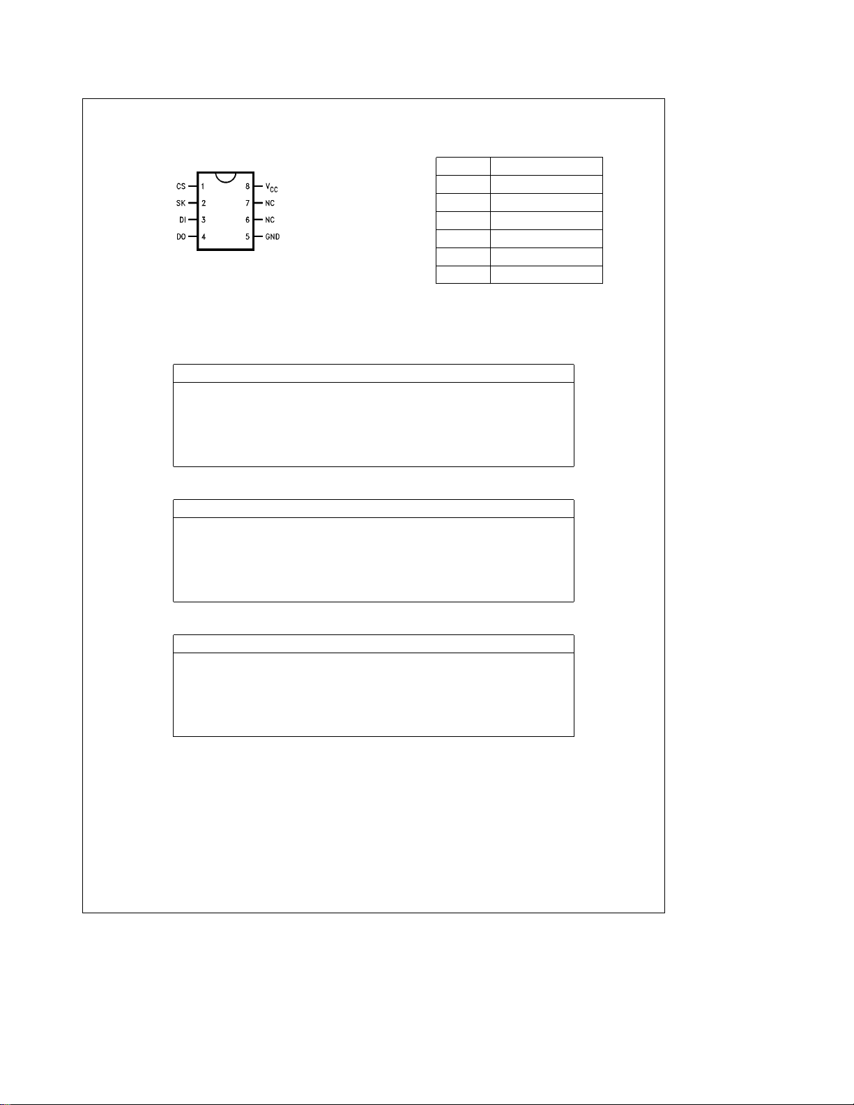
Connection Diagram
Dual-in-Line Package (N)
8-Pin SO (M8) and 8-Pin TSSOP (MT8)
Top View
See NS Package Number
N08E and M08A
Ordering Information
Pin Description
CS Chip Select
SK Serial Data Clock
DI Serial Data Input
TL/D/11778– 2
Commercial Temperature Range (0§Ctoa70§C)
Order Number
NM93C06LZN/NM93C46LZN
NM93C56LZN/NM93C66LZN
NM93C06LZM8/NM93C46LZM8
NM93C56LZM8/NM93C66LZM8
NM93C06LZMT8/NM93C46LZMT8
NM93C56LZMT8/NM93C66LZMT8
Extended Temperature Range (b40§Ctoa85§C)
Order Number
NM93C06LZEN/NM93C46LZEN
NM93C56LZEN/NM93C66LZEN
NM93C06LZEM8/NM93C46LZEM8
NM93C56LZEM8/NM93C66LZEM8
NM93C06LZEMT8/NM93C46LZEMT8
NM93C56LZEMT8/NM93C66LZEMT8
DO Serial Data Output
GND Ground
V
CC
Pin Names
Power Supply
Automotive Temperature Range (b40§Ctoa125§C)
Order Number
NM93C06LZVN/NM93C46LZVN
NM93C56LZVN/NM93C66LZVN
NM93C06LZVM8/NM93C46LZVM8
NM93C56LZVM8/NM93C66LZVM8
NM93C06LZVMT8/NM93C46LZVMT8
NM93C56LZVMT8/NM93C66LZVMT8
http://www.national.com 2

LOW VOLTAGE (2.7Vs4.5V) SPECIFICATIONS
Absolute Maximum Ratings
(Note 1)
If Military/Aerospace specified devices are required,
please contact the National Semiconductor Sales
Office/Distributors for availability and specifications.
Ambient Storage Temperature
All Input or Output Voltage
with Respect to Ground V
Lead Temperature (Soldering, 10 sec.)
b
65§Ctoa150§C
a
1tob0.3V
CC
a
300§C
Operating Conditions
Ambient Operating Temperature
NM93C06LZ/46LZ/56LZ/66LZ 0
NM93C06LZE/46LZE/56LZE/66LZE
NM93C06LZV/46LZV/56LZV/66LZV
Power Supply (V
) Range 2.7V to 4.5V
CC
Ctoa70§C
§
b
40§Ctoa85§C
b
40§Ctoa125§C
ESD Rating 2000V
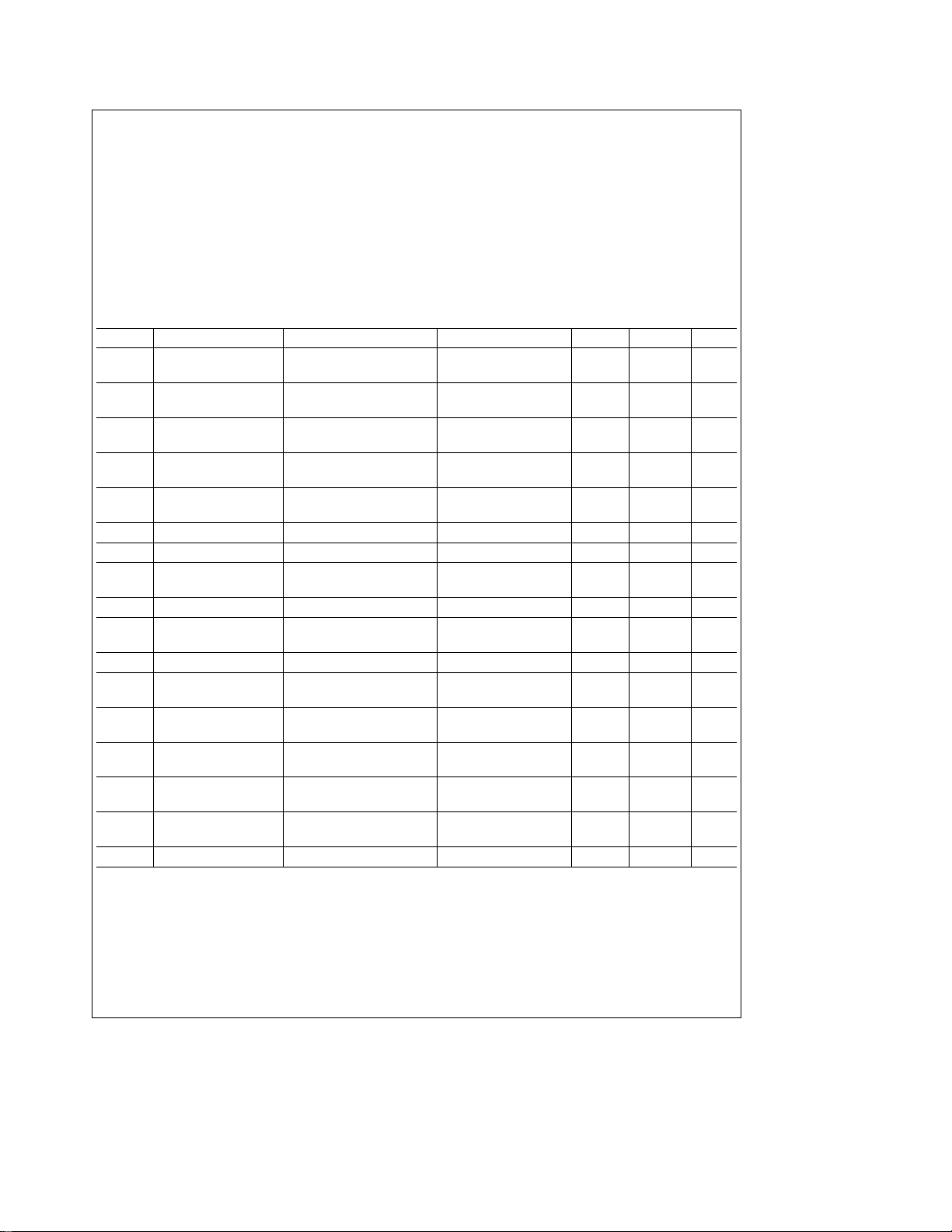
DC and AC Electrical Characteristics
Symbol Parameter Part Number Conditions Min Max Units
I
CC1
I
CC3
I
IL
I
OL
V
IL2
V
IH2
V
OL2
V
OH2
f
SK
t
SKH
t
SKL
t
SKS
t
CS
t
CSS
t
DH
t
DIS
t
CSH
t
DIH
t
PD1
t
PD0
t
SV
t
DF
t
WP
Operating Current NM93C06/46/56/66LZ CSeVIH,SKe250 kHz 1
CMOS Input Levels NM93C06/46/56/66LZE/V 1
Standby Current NM93C06/46/56/66LZ CSe0V 1
NM93C06/46/56/66LZE/V 1
Input Leakage NM93C06/46/56/66LZ V
NM93C06/46/56/66LZE/V
Output Leakage NM93C06/46/56/66LZ V
NM93C06/46/56/66LZE/V
Input Low Voltage 2VsV
Input High Voltage 2VsV
Output Low Voltage I
Output High Voltage I
e
0V to V
OL
OH
IN
IN
e
e
eb
CC
0V to V
CC
s
4.5V
CC
s
4.5V 0.8 V
CC
b
100
b
100
b
0.1 0.15 V
CCVCC
a
a
10 mA 0.2 V
10 mA 0.9 V
CC
100
100
SK Clock Frequency NM93C06/46/56/66LZ 0 250
NM93C06/46/56/66LZE/V 0 250
SK High Time NM93C06/46/56/66LZ (Note 2) 1
NM93C06/46/56/66LZE/V 1
SK Low Time NM93C06/46/56/66LZ (Note 2) 1
NM93C06/46/56/66LZE/V 1
SK Setup Time NM93C06/46/56/66LZ Relative to CS 50
NM93C06/46/56/66LZE/V 50
Minimum CS Low Time NM93C06/46/56/66LZ (Note 3) 1
NM93C06/46/56/66LZE/V 1
CS Setup Time NM93C06/46/56/66LZ Relative to SK 0.2
NM93C06/46/56/66LZE/V 0.2
mA
mA
CC
a
1V
kHz
nA
nA
ms
ms
ms
ms
ms
DO Hold Time Relative to SK 70 ns
DI Setup Time NM93C06/46/56/66LZ Relative to SK 0.4
NM93C06/46/56/66LZE/V 0.4
ms
CS Hold Time Relative to SK 0 ms
DI Hold Time Relative to SK 0.4 ms
Output Delay to ‘‘1’’ NM93C06/46/56/66LZ AC Test 2
NM93C06/46/56/66LZE/V 2
Output Delay to ‘‘0’’ NM93C06/46/56/66LZ AC Test 2
NM93C06/46/56/66LZE/V 2
CS to Status Valid NM93C06/46/56/66LZ AC Test 1
NM93C06/46/56/66LZE/V 1
CS to DO NM93C06/46/56/66LZ AC Test 0.4
in TRI-STATE
É
NM93C06/46/56/66LZE/V CSeV
Write Cycle Time NM93C06/46/56/66LZ V
IL
e
2.7V 15 ms
CC
0.4
ms
ms
ms
ms
V
V
http://www.national.com3
STANDARD VOLTAGE (4.5VsV
s
5.5V) SPECIFICATIONS
CC
Absolute Maximum Ratings
(Note 1)
If Military/Aerospace specified devices are required,
please contact the National Semiconductor Sales
Office/Distributors for availability and specifications.
Ambient Storage Temperature
All Input or Output Voltage
with Respect to Ground V
Lead Temperature (Soldering, 10 sec.)
b
65§Ctoa150§C
a
1tob0.3V
CC
a
300§C
Operating Conditions
Ambient Operating Temperature
NM93C06LZ/46LZ/56LZ/66LZ 0
NM93C06LZE/46LZE/56LZE/66LZE
NM93C06LZV/46LZV/56LZV/66LZV
Power Supply (V
) Range 4.5V to 5.5V
CC
Ctoa70§C
§
b
40§Ctoa85§C
b
40§Ctoa125§C
ESD Rating 2000V
s
DC and AC Electrical Characteristics: 4.5V
s
V
5.5V
CC
Symbol Parameter Part Number Conditions Min Max Units
I
CC1
I
CC2
I
CC3
I
IL
I
OL
V
IL
V
IH
V
OL1
V
OH1
V
OL2
V
OH2
f
SK
t
SKH
t
SKL
t
CS
t
CSS
t
DH
Operating Current NM93C06/46/56/66LZ CSeVIH,SKe1 MHz 2
CMOS Input Levels NM93C06/46/56/66LZE/V SK
e
1 MHz 2
Operating Current NM93C06/46/56/66LZ CSeVIH,SKe1 MHz 3
TTL Input Levels NM93C06/46/56/66LZE/V 3
Standby Current NM93C06/46/56/66LZ CSe0V 50
NM93C06/46/56/66LZE/V 50
Input Leakage NM93C06/46/56/66LZ V
NM93C06/46/56/66LZE/V
Output Leakage NM93C06/46/56/66LZ V
NM93C06/46/56/66LZE/V
e
0V to V
IN
e
IN
0V to V
CC
CC
Input Low Voltage
Input High Voltage 2 V
Output Low Voltage NM93C06/46/56/66LZ I
NM93C06/46/56/66LZE/V I
Output High Voltage I
Output Low Voltage NM93C06/46/56/66LZ I
NM93C06/46/56/66LZE/V
Output High Voltage I
e
2.1 mA 0.4
OL
e
2.1 mA 0.4
OH
eb
400 mA 2.4 V
OL
e
10 mA
OL
eb
10 mA 0.9 V
OH
b
2.5 2.5
b
10 10
b
2.5 2.5
b
10 10
b
0.1 0.8 V
CC
0.2
CC
SK Clock Frequency NM93C06/46/56/66LZ 0 1
NM93C06/46/56/66LZE/V 0 1
mA
mA
mA
nA
nA
a
1V
MHz
SK High Time NM93C06/46/56/66LZ 250
NM93C06/46/56/66LZE/V 300
SK Low Time NM93C06/46/56/66LZ 250
NM93C06/46/56/66LZE/V 250
Minimum CS Low Time NM93C06/46/56/66LZ (Note 3) 250
NM93C06/46/56/66LZE/V 250
CS Setup Time NM93C06/46/56/66LZ Relative to SK 50
NM93C06/46/56/66LZE/V 50
DO Hold Time Relative to SK 70 ns
V
V
V
ns
ns
ns
ns
http://www.national.com 4

STANDARD VOLTAGE (4.5VsV
s
5.5V) SPECIFICATIONS (Continued)
CC
DC and AC Electrical Characteristics V
e
5.0Vg10% unless otherwise specified (Continued)
CC
Symbol Parameter Part Number Conditions Min Max Units
t
t
t
t
t
t
t
t
DIS
CSH
DIH
PD1
PD0
SV
DF
WP
DI Setup Time NM93C06/46/56/66LZ Relative to SK 100
NM93C06/46/56/66LZE/V 200
ns
CS Hold Time Relative to SK 0 ns
DI Hold Time Relative to SK 20 ns
Output Delay to ‘‘1’’ NM93C06/46/56/66LZ AC Test 500
NM93C06/46/56/66LZE/V 500
Output Delay to ‘‘0’’ NM93C06/46/56/66LZ AC Test 500
NM93C06/46/56/66LZE/V 500
CS to Status Valid NM93C06/46/56/66LZ AC Test 500
NM93C06/46/56/66LZE/V 500
CS to DO in TRI-STATE NM93C06/46/56/66LZ AC Test 100
NM93C06/46/56/66LZE/V CSeV
IL
100
ns
ns
ns
ns
Write Cycle Time 10 ms
AC Test Conditions
Output Load: 1 TTL Gate and C
VCCRange AC Test Conditions
4.5VkV
k
5.5V Input Pulse Levels 0.8V and 2.0V
CC
Timing Measurement Level (V
Timing Measurement Level (V
(TTL Load Condition:
2.7VkV
e
I
2.1 mA, I
OL
k
4.5V Input Pulse Levels 0.3V and 0.8 V
CC
Timing Measurement Level (VIL/VIH) 0.4V and 1.6V
OH
eb
Timing Measurement Level (V
(CMOS Load Condition:
e
I
10 mA, I
OL
OH
eb
L
0.4 mA)
10 mA)
e
100 pF
) 0.9V and 1.9V
IL/VIH
OL/VOH
OL/VOH
) 0.8V and 2.0V
CC
) 0.8V and 1.6V
Capacitance T
e
25§C, fe1 MHz
A
Symbol Test Max Units
C
OUT
C
IN
Note 1: Stress above those listed under ‘‘Absolute Maximum Ratings’’ may cause permanent damage to the device. This is a stress rating only, and functional
operation of the device at these or any other conditions above those indicated in the operational sections of the specification is not implied. Exposure to absolute
maximum rating conditions for extended periods may affect device reliability.
Note 2: Minimum V
These are regarded as test mode commands and are only guaranteed to V
Note 3: CS must be brought low for a minimum of 1 t
CC
Output Capacitance 5 pF
Input Capacitance 5 pF
requirements: All functional modes are guaranteed to full operation at V
between consecutive instruction cycles.
CS
t
2.5V.
CC
t
2V except the bulk programming op-codes ERAL and WRAL.
CC
http://www.national.com5

Functional Description
The NM93C06/C46/C56/C66LZ devices have 7 instructions as described below. Note that the MSB of any instruction is a ‘‘1’’ and is viewed as a start bit in the interface
sequence. For the C06LZ and C46LZ the next 8 bits carry
the op code and the 6-bit address for register selection. For
the C56LZ and C66LZ the next 10 bits carry the op code
and the 8-bit address for register selection.
Read (READ): The READ instruction outputs serial data on
the DO pin. After the READ instruction is received, the instruction and address are decoded, followed by data transfer from the selected memory register into a serial-out shift
register. A dummy bit (logical 0) precedes the 16-bit data
output string. Output data changes are initiated by a low to
high transition of the SK clock.
Erase/Write Enable (EWEN): When V
part, it powers up in the Erase/Write Disable (EWDS) state.
Therefore, all programming modes must be preceded by an
Erase/Write Enable (EWEN) instruction. Once an Erase/
Write Enable instruction is executed, programming remains
enabled until an Erase/Write Disable (EWDS) instruction is
executed or until V
Erase (ERASE): The ERASE instruction will program all bits
in the specified register to the logical ‘‘1’’ state. CS is
brought low following the loading of the last address bit.
This falling edge of the CS pin initiates the self-timed programming cycle.
The DO pin indicates the READY/BUSY status of the chip.
e
DO
logical ‘‘0’’ indicates that programming is still in progress. DO
address specified in the instruction, has been erased, and
the part is ready for another instruction.
e
is removed from the part.
CC
logical ‘‘1’’ indicates that the register, at the
is applied to the
CC
Write (WRITE): The WRITE instruction is followed by 16
bits of data to be written into the specified address. After the
last bit of data is put on the data-in (DI) pin, CS must be
brought low before the next rising edge of the SK clock.
This falling edge of CS initiates the self-timed programming
cycle. The DO pin indicates the READY/BUSY status of the
chip if CS is brought high after a minimum of 250 ns (t
e
DO
logical 0 indicates that programming is still in progress. DO
specified in the instruction has been written with the data
pattern specified in the instruction and the part is ready for
another instruction.
Erase All (ERAL): The ERAL instruction will simultaneously
program all registers in the memory array and set each bit to
the logical ‘‘1’’ state. The Erase All cycle is identical to the
ERASE cycle except for the different op code. As in the
ERASE mode, the DO pin indicates the READY/BUSY
status of the chip. The ERASE ALL instruction is not required, see note below.
Write All (WRAL): The WRAL instruction will simultaneously program all registers with the data pattern specified in the
instruction. As in the WRITE mode, the DO pin indicates the
READY/BUSY status of the chip.
Erase/Write Disable (EWDS): To protect against accidental data disturb, the (EWDS) instruction disables all programming modes and should follow all programming operations. Execution of a READ instruction is independent of
both the EWEN and EWDS instructions.
Note: The NM93C06/C46/C56/C66LZ devices do not require an ‘‘ERASE’’
e
1 indicates that the register at the address
or ‘‘ERASE ALL’’ prior to the ‘‘WRITE’’ or ‘‘WRITE ALL’’ instructions.
CS
).
Instruction Set for the NM93C06LZ and NM93C46LZ
Instruction SB Op Code Address Data Comments
READ 1 10 A5– A0 Read data stored in memory, at specified address
EWEN 1 00 11XXXX Write enable must precede all programming modes
EWDS 1 11 A5 – A0 Erase register A5, A4, A3, A2, A1, A0
WRITE 1 01 A5 – A0 D15 – D0 Writes register
ERAL 1 00 10XXXX Erases all registers
WRAL 1 00 01XXXX D15– D0 Writes all registers
EWDS 1 00 00XXXX Disables all programming instructions
Instruction Set for the NM93C56LZ and NM93C66LZ
Instruction SB Op Code Address Data Comments
READ 1 10 A7– A0 Read data stored in memory, at specified address
EWEN 1 00 11XXXXXX Write enable must precede all programming modes
EWDS 1 11 A7–A0 Erase selected register
ERAL 1 00 10XXXXXX Erases all registers
WRITE 1 01 A7–A0 D15 – D0 Write register if address is unprotected
WRAL 1 00 01XXXXXX D15– D0 Writes all registers
EWDS 1 00 00XXXXXX Disables all programming instructions
http://www.national.com 6

Timing Diagrams
Synchronous Data Timing
²
t
is not needed if DIeVILwhen CS is going active (HIGH).
SKS
*Address bits A5 and A4 become ‘‘don’t care’’ for NM93C06LZ.
Address bit A7 becomes a ‘‘don’t care’’ for NM93C56LZ.
TL/D/11778– 3
READ
TL/D/11778– 4
EWEN
*The NM93C56LZ and NM93C66LZ require a minimum of 11 clock cycles. The NM93C06LZ and NM93C46LZ require a minimum of 9 clock cycles.
http://www.national.com7
TL/D/11778– 5

Timing Diagrams (Continued)
EWDS
*The NM93C56LZ and NM93C66LZ require a minimum of 11 clock cycles. The NM93C06LZ and NM93C46LZ require a minimum of 9 clock cycles.
WRITE
*Address bits A5 and A4 become ‘‘don’t care’’ for NM93C06LZ.
Address bit A7 becomes a ‘‘don’t care’’ for NM93C56LZ.
WRAL
TL/D/11778– 6
TL/D/11778– 7
http://www.national.com 8
TL/D/11778– 8

Timing Diagrams (Continued)
ERASE
*Address bits A5 and A4 become ‘‘don’t care’’ for NM93C06LZ.
Address bit A7 becomes a ‘‘don’t care’’ for NM93C56LZ.
TL/D/11778– 9
ERAL
TL/D/11778– 10
http://www.national.com9

Physical Dimensions inches (millimeters) unless otherwise noted
Molded Small Out-Line Package (M8)
NS Package Number M08A
http://www.national.com 10

Physical Dimensions inches (millimeters) unless otherwise noted (Continued)
Note: Unless otherwise specified
1. Reference JEDEC Registration M0-153, Variation AA, Dated 7/93
8-Pin Molded TSSOP, JEDEC (MT8)
NS Package Number MTC08
http://www.national.com11

Physical Dimensions inches (millimeters) unless otherwise noted (Continued)
8-Lead Molded Dual-In-Line Package (N)
NS Package Number N08E
and Extended Voltage (2.7V to 5.5V) (MICROWIRE Bus Interface)
LIFE SUPPORT POLICY
NATIONAL’S PRODUCTS ARE NOT AUTHORIZED FOR USE AS CRITICAL COMPONENTS IN LIFE SUPPORT
DEVICES OR SYSTEMS WITHOUT THE EXPRESS WRITTEN APPROVAL OF THE PRESIDENT OF NATIONAL
SEMICONDUCTOR CORPORATION. As used herein:
1. Life support devices or systems are devices or 2. A critical component is any component of a life
systems which, (a) are intended for surgical implant support device or system whose failure to perform can
into the body, or (b) support or sustain life, and whose be reasonably expected to cause the failure of the life
failure to perform, when properly used in accordance support device or system, or to affect its safety or
with instructions for use provided in the labeling, can effectiveness.
be reasonably expected to result in a significant injury
to the user.
National Semiconductor National Semiconductor National Semiconductor National Semiconductor
Corporation Europe Hong Kong Ltd. Japan Ltd.
1111 West Bardin Road Fax:
Arlington, TX 76017 Email: europe.support@nsc.com Ocean Centre, 5 Canton Rd. Fax: 81-043-299-2408
Tel: 1(800) 272-9959 Deutsch Tel:
Fax: 1(800) 737-7018 English Tel:
http://www.national.com
NM93C06LZ/C46LZ/C56LZ/C66LZ 256-/1024-/2048-/4096-Bit Serial EEPROM with Zero Power
National does not assume any responsibility for use of any circuitry described, no circuit patent licenses are implied and National reserves the right at any time without notice to change said circuitry and specifications.
Fran3ais Tel:
Italiano Tel:a49 (0) 180-534 16 80 Fax: (852) 2736-9960
a
49 (0) 180-530 85 86 13th Floor, Straight Block, Tel: 81-043-299-2308
a
49 (0) 180-530 85 85 Tsimshatsui, Kowloon
a
49 (0) 180-532 78 32 Hong Kong
a
49 (0) 180-532 93 58 Tel: (852) 2737-1600
 Loading...