

Page 1
MM54HC237/MM74HC237
3-to-8 Line Decoder With Address Latches
General Description
These devices utilize advanced silicon-gate CMOS technology, to implement a three-to-eight line decoder with latches
on the three address inputs. When GL
high, the address present at the select inputs (A, B and C) is
stored in the latches. As long as GL
dress changes will be recognized. Output enable controls,
G1 and G2
the select or latch-enable inputs. All of the outputs are low
unless G1 is high and G2
ed for the implementation of glitch-free decoders in storedaddress applications in bus oriented systems.
, control the state of the outputs independently of
is low. The ’HC237 is ideally suit-
goes from low to
remains high no ad-
The 54HC/74HC logic family is speed, function and pin-out
compatible with the standard 54LS/74LS logic family. All
inputs are protected from damage due to static discharge by
diodes to V
and ground.
CC
Features
Y
Typical propagation delay: 20 ns
Y
Wide supply range: 2– 6V
Y
Latched inputs for easy interfacing
Y
Fanout of 10 LS-TTL loads
MM54HC237/MM74HC237 3-to-8 Line Decoder With Address Latches
January 1988
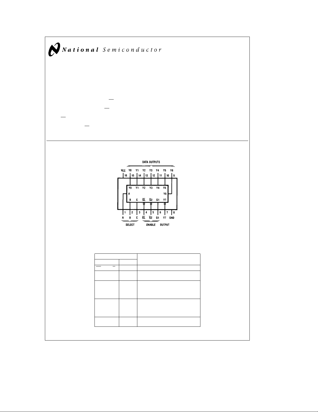
Connection Diagram
Truth Table
ENABLE SELECT
GL G1 G2 C B A Y0 Y1 Y2 Y3 Y4 Y5 Y6 Y7
XXHXXXLLLLLLLL
XLXXXXLLLLLLLL
LHLLLLHLLLLLLL
LHLLLHLHLLLLLL
LHLLHLLLHLLLLL
LHLLHHLLLHLLLL
LHLHLLLLLLHLLL
LHLHLHLLLLLHLL
LHLHHLLLLLLLHL
LHLHHHLLLLLLLH
HHLXXX
Hehigh level, Lelow level, Xeirrelevant
Dual-In-Line Package
Top View
Order Number MM54HC237 or MM74HC237
INPUTS
Output corresponding to stored
address, L; all others, H
OUTPUTS
TL/F/5326– 1
C
1995 National Semiconductor Corporation RRD-B30M105/Printed in U. S. A.
TL/F/5326
Page 2
Absolute Maximum Ratings (Notes1&2)
Operating Conditions
If Military/Aerospace specified devices are required,
please contact the National Semiconductor Sales
Office/Distributors for availability and specifications.
Supply Voltage (V
CC
)
DC Input Voltage (VIN)
DC Output Voltage (V
OUT
)
Clamp Diode Current (IIK,IOK)
DC Output Current, per pin (I
OUT
)
DC VCCor GND Current, per pin (ICC)
Storage Temperature Range (T
STG
b
b
)
b
0.5 toa7.0V
1.5 to V
CC
0.5 to V
CC
g
g
b
g
65§Ctoa150§C
a
1.5V
a
0.5V
20 mA
25 mA
50 mA
Supply Voltage (V
)26V
CC
DC Input or Output Voltage 0 V
(V
IN,VOUT
)
Operating Temp. Range (TA)
MM74HC
MM54HC
Input Rise or Fall Times
e
V
2.0V(tr,tf) 1000 ns
CC
e
V
4.5V 500 ns
CC
e
V
6.0V 400 ns
CC
Power Dissipation (PD)
(Note 3) 600 mW
S.O. Package only 500 mW
Lead Temperature
(T
) (Soldering 10 seconds) 260§C
L
DC Electrical Characteristics (Note 4)
Symbol Parameter Conditions V
CC
A
e
T
25§C
Typ Guaranteed Limits
V
IH
Minimum High Level 2.0V 1.5 1.5 1.5 V
Input Voltage 4.5V 3.15 3.15 3.15 V
6.0V 4.2 4.2 4.2 V
V
IL
Maximum Low Level 2.0V 0.5 0.5 0.5 V
Input Voltage** 4.5V 1.35 1.35 1.35 V
6.0V 1.8 1.8 1.8 V
V
OH
Minimum High Level V
Output Voltage
e
VIHor V
l
IN
I
OUT
IL
s
20 mA 2.0V 2.0 1.9 1.9 1.9 V
l
4.5V 4.5 4.4 4.4 4.4 V
6.0V 6.0 5.9 5.9 5.9 V
e
V
VIHor V
IN
I
l
OUT
I
l
OUT
l
IN
I
OUT
e
V
OL
Maximum Low Level V
Output Voltage
IL
s
4.0 mA 4.5V 4.2 3.98 3.84 3.7 V
l
s
5.2 mA 6.0V 5.7 5.48 5.34 5.2 V
l
VIHor V
IL
s
20 mA 2.0V 0 0.1 0.1 0.1 V
l
4.5V 0 0.1 0.1 0.1 V
6.0V 0 0.1 0.1 0.1 V
e
V
VIHor V
IN
I
l
OUT
I
l
OUT
I
IN
I
CC
Note 1: Absolute Maximum Ratings are those values beyond which damage to the device may occur.
Note 2: Unless otherwise specified all voltages are referenced to ground.
Note 3: Power Dissipation temperature derating Ð plastic ‘‘N’’ package:
Note 4: For a power supply of 5V
designing with this supply. Worst case V
I
**V
Maximum Input V
Current
Maximum Quiescent V
Supply Current I
, and IOZ) occur for CMOS at the higher voltage and so the 6.0V values should be used.
CC
limits are currently tested at 20% of VCC. The above VILspecification (30% of VCC) will be implemented no later than Q1, CY’89.
IL
e
IN
e
IN
OUT
g
10% the worst case output voltages (VOH, and VOL) occur for HC at 4.5V. Thus the 4.5V values should be used when
and VILoccur at V
IH
IL
s
4.0 mA 4.5V 0.2 0.26 0.33 0.4 V
l
s
5.2 mA 6.0V 0.2 0.26 0.33 0.4 V
l
VCCor GND 6.0V
g
0.1
VCCor GND 6.0V 8.0 80 160 mA
e
0 mA
b
12 mW/§C from 65§Cto85§C; ceramic ‘‘J’’ package:b12 mW/§C from 100§Cto125§C.
e
5.5V and 4.5V respectively. (The VIHvalue at 5.5V is 3.85V.) The worst case leakage current (IIN,
CC
74HC 54HC
eb
T
40 to 85§CT
A
g
1.0
Min Max Units
V
§
§
Units
b
b
40
55
eb
A
55 to 125§C
g
CC
a
85
a
125
1.0 mA
C
C
2
Page 3

AC Electrical Characteristics V
CC
5V, T
e
A
25§C, C
e
L
15 pF, t
e
Symbol Parameter Conditions Typ
t
PLH
t
PLH
t
PLH
t
PHL
t
PLH
t
PHL
t
S
t
H
t
W
Maximum Propagation Delay A, B or C to any Y Output 20 41 ns
Maximum Propagation Delay A, B or C to any Y Output 16 32 ns
Maximum Propagation GL to any Y Output 22 44 ns
Maximum Propagation Delay GL to any Y Output 17 33 ns
Maximum Propagation Delay G1 or G2 to Output 16 35 ns
Maximum Propagation Delay G1 or G2 to Output 14 25 ns
Minimum Set Up Time at A, B and C Inputs 10 20 ns
Minimum Hold Time at A, B and C Inputs
Minimum Pulse Width of Enabling Pulse at GL 916ns
e
e
t
6ns
r
f
Guaranteed
Limit
b
30 ns
Units
AC Electrical Characteristics C
e
L
50 pF, t
Symbol Parameter Conditions V
t
PLH
t
PLH
t
PLH
t
PHL
t
PLH
t
PHL
t
S
t
H
t
W
t
TLH,tTHL
C
PD
C
IN
Note 5: CPDdetermines the no load dynamic power consumption, P
Maximum Propagation 2.0V 100 235 296 350 ns
Delay, A, B or C to any Y Output 4.5V 24 47 59 70 ns
Maximum Propagation 2.0V 80 185 233 276 ns
Delay, A, B or C to any Y Output 4.5V 19 37 47 55 ns
Maximum Propagation 2.0V 125 250 315 373 ns
GL to any Y Output 4.5V 25 50 63 75 ns
Maximum Propagation Delay 2.0V 95 190 239 283 ns
GL
to any Y Output 4.5V 19 38 48 75 ns
Maximum Propagation 2.0V 100 200 252 298 ns
Delay, G1 or G
2 to Output 4.5V 20 40 50 60 ns
Maximum Propagation 2.0V 73 145 183 216 ns
Delay G1 or G
2 to Output 4.5V 15 29 37 43 ns
Minimum Set Up Time 2.0V 100 125 150 ns
at A, B and C Inputs 4.5V 20 25 30 ns
Minimum Hold Time 2.0V 0 0 0 ns
at A, B and C Inputs 4.5V 0 0 0 ns
Minimum Pulse Width 2.0V 30 80 100 120 ns
of Enabling Pulse at GL
Maximum Output Rise 2.0V 30 75 95 110 ns
and Fall Time 4.5V 8 15 19 22 ns
Power Dissipation 75 pF
Capacitance (Note 5)
Maximum Input 5 10 10 10 pF
Capacitance
e
D
e
e
t
6 ns (unless otherwise specified)
r
CC
f
e
T
25§C
A
74HC 54HC
eb
T
40 to 85§CT
A
A
eb
55 to 125§C
Typ Guaranteed Limits
6.0V 20 40 50 60 ns
6.0V 17 31 40 47 ns
6.0V 20 43 54 63 ns
6.0V 16 32 41 48 ns
6.0V 17 34 43 51 ns
6.0V 12 25 31 37 ns
6.0V 17 21 25 ns
6.0V 0 0 0 ns
4.5V 10 16 20 24 ns
6.0V 9 14 18 20 ns
6.0V 7 13 16 19 ns
2
CPDV
faICCVCC, and the no load dynamic current consumption, I
CC
e
CPDVCCfaICC.
S
Units
3
Page 4

Functional Block Diagram
Typical Application
TL/F/5326– 2
6-Line to 64-Line Decoder with Input Address Storage
4
TL/F/5326– 3
Page 5

Physical Dimensions inches (millimeters)
Ceramic Dual-In-Line Package (J)
Order Number MM54HC237J or MM74HC237J
NS Package Number J16A
5
Page 6

Physical Dimensions inches (millimeters) (Continued)
Molded Dual-In-Line Package (N)
Order Number MM74HC237N
NS Package Number N16E
LIFE SUPPORT POLICY
MM54HC237/MM74HC237 3-to-8 Line Decoder With Address Latches
NATIONAL’S PRODUCTS ARE NOT AUTHORIZED FOR USE AS CRITICAL COMPONENTS IN LIFE SUPPORT
DEVICES OR SYSTEMS WITHOUT THE EXPRESS WRITTEN APPROVAL OF THE PRESIDENT OF NATIONAL
SEMICONDUCTOR CORPORATION. As used herein:
1. Life support devices or systems are devices or 2. A critical component is any component of a life
systems which, (a) are intended for surgical implant support device or system whose failure to perform can
into the body, or (b) support or sustain life, and whose be reasonably expected to cause the failure of the life
failure to perform, when properly used in accordance support device or system, or to affect its safety or
with instructions for use provided in the labeling, can effectiveness.
be reasonably expected to result in a significant injury
to the user.
National Semiconductor National Semiconductor National Semiconductor National Semiconductor
Corporation Europe Hong Kong Ltd. Japan Ltd.
1111 West Bardin Road Fax: (
Arlington, TX 76017 Email: cnjwge@tevm2.nsc.com Ocean Centre, 5 Canton Rd. Fax: 81-043-299-2408
Tel: 1(800) 272-9959 Deutsch Tel: (
Fax: 1(800) 737-7018 English Tel: (
National does not assume any responsibility for use of any circuitry described, no circuit patent licenses are implied and National reserves the right at any time without notice to change said circuitry and specifications.
Fran3ais Tel: (
Italiano Tel: (
a
49) 0-180-530 85 86 13th Floor, Straight Block, Tel: 81-043-299-2309
a
49) 0-180-530 85 85 Tsimshatsui, Kowloon
a
49) 0-180-532 78 32 Hong Kong
a
49) 0-180-532 93 58 Tel: (852) 2737-1600
a
49) 0-180-534 16 80 Fax: (852) 2736-9960
 Loading...