

Page 1
MM54HC190/MM74HC190 Synchronous
Decade Up/Down Counters with Mode
Control MM54HC191/MM74HC191
Synchronous Binary Up/Down Counters
with Mode Control
General Description
These high speed synchronous counters utilize advanced
silicon-gate CMOS technology. They possess the high noise
immunity and low power consumption of CMOS technology,
along with the speeds of low power Schottky TTL.
These circuits are synchronous, reversible, up/down counters. The MM54HC191/MM74HC191 are 4-bit binary counters and the MM54HC190/MM74HC190 are BCD counters.
Synchronous operation is provided by having all flip-flops
clocked simultaneously, so that the outputs change simultaneously when so instructed by the steering logic. This mode
of operation eliminates the output counting spikes normally
associated with asynchronous (ripple clock) counters.
The outputs of the four master-slave flip-flops are triggered
on a low-to-high level transition of the clock input, if the
enable input is low. A high at the enable input inhibits counting. The direction of the count is determined by the level of
the down/up input. When low, the counter counts up and
when high, it counts down.
These counters are fully programmable; that is, the outputs
may be preset to either level by placing a low on the load
input and entering the desired data at the data inputs. The
output will change independent of the level of the clock input. This feature allows the counters to be used as modulo-
N dividers by simply modifying the count length with the
preset inputs.
Two outputs have been made available to perform the cascading function: ripple clock and maximum/minimum count.
The latter output produces a high-level output pulse with a
duration approximately equal to one complete cycle of the
clock when the counter overflows or underflows. The ripple
clock output produces a low-level output pulse equal in
width to the low-level portion of the clock input when an
overflow or underflow condition exists. The counters can be
easily cascaded by feeding the ripple clock output to the
enable input of the succeeding counter if parallel clocking is
used, or to the clock input if parallel enabling is used. The
maximum/minimum count output can be used to accomplish look-ahead for high-speed operation.
Features
Y
Level changes on Enable or Down/Up can be made regardless of the level of the clock input
Y
Wide power supply range: 2–6V
Y
Low quiescent supply current: 80 mA maximum
(74HC Series)
Y
Low input current: 1 mA maximum
MM54HC190/MM74HC190/MM54HC191/MM74HC191
January 1988
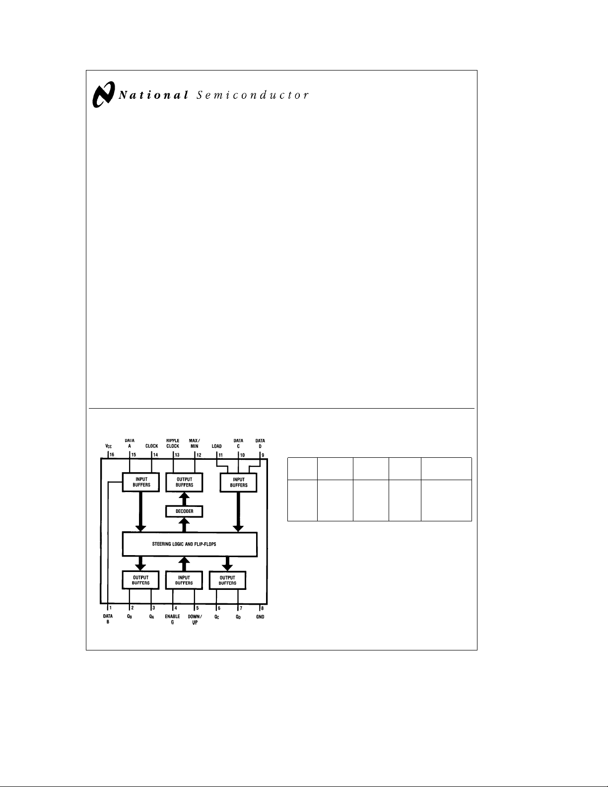
Connection Diagram
Dual-In-Line Package
Load
Order Number MM54HC190/191 or MM74HC190/191
Top View
C
1995 National Semiconductor Corporation RRD-B30M105/Printed in U. S. A.
TL/F/5322
TL/F/5322– 1
Enable Down/
GUp
HL L
HL H
L X X X Load
H H X X No Change
Asynchronous inputs Low input to load sets Q
e
Q
B, Q
B
Clock Function
e
C, and Q
C
e
D
Count Up
Count Down
e
A,
A
u
u
D
Page 2
Absolute Maximum Ratings (Notes1&2)
Operating Conditions
If Military/Aerospace specified devices are required,
please contact the National Semiconductor Sales
Office/Distributors for availability and specifications.
Supply Voltage (V
CC
)
DC Input Voltage (VIN)
DC Output Voltage (V
OUT
)
Clamp Diode Current (IIK,IOK)
DC Output Current, per pin (I
OUT
)
DC VCCor GND Current, per pin (ICC)
Storage Temperature Range (T
STG
b
b
)
b
0.5 toa7.0V
1.5 to V
CC
0.5 to V
CC
g
g
b
g
65§Ctoa150§C
a
1.5V
a
0.5V
20 mA
25 mA
50 mA
Power Dissipation (PD)
Supply Voltage (V
)26V
CC
DC Input or Output Voltage 0 V
(V
IN,VOUT
)
Operating Temp. Range (TA)
MM74HC
MM54HC
Input Rise or Fall Times
e
V
2.0V(tr,tf) 1000 ns
CC
e
V
4.5V 500 ns
CC
e
V
6.0V 400 ns
CC
(Note 3) 600 mW
S.O. Package only 500 mW
Lead Temp. (T
) (Soldering 10 seconds) 260§C
L
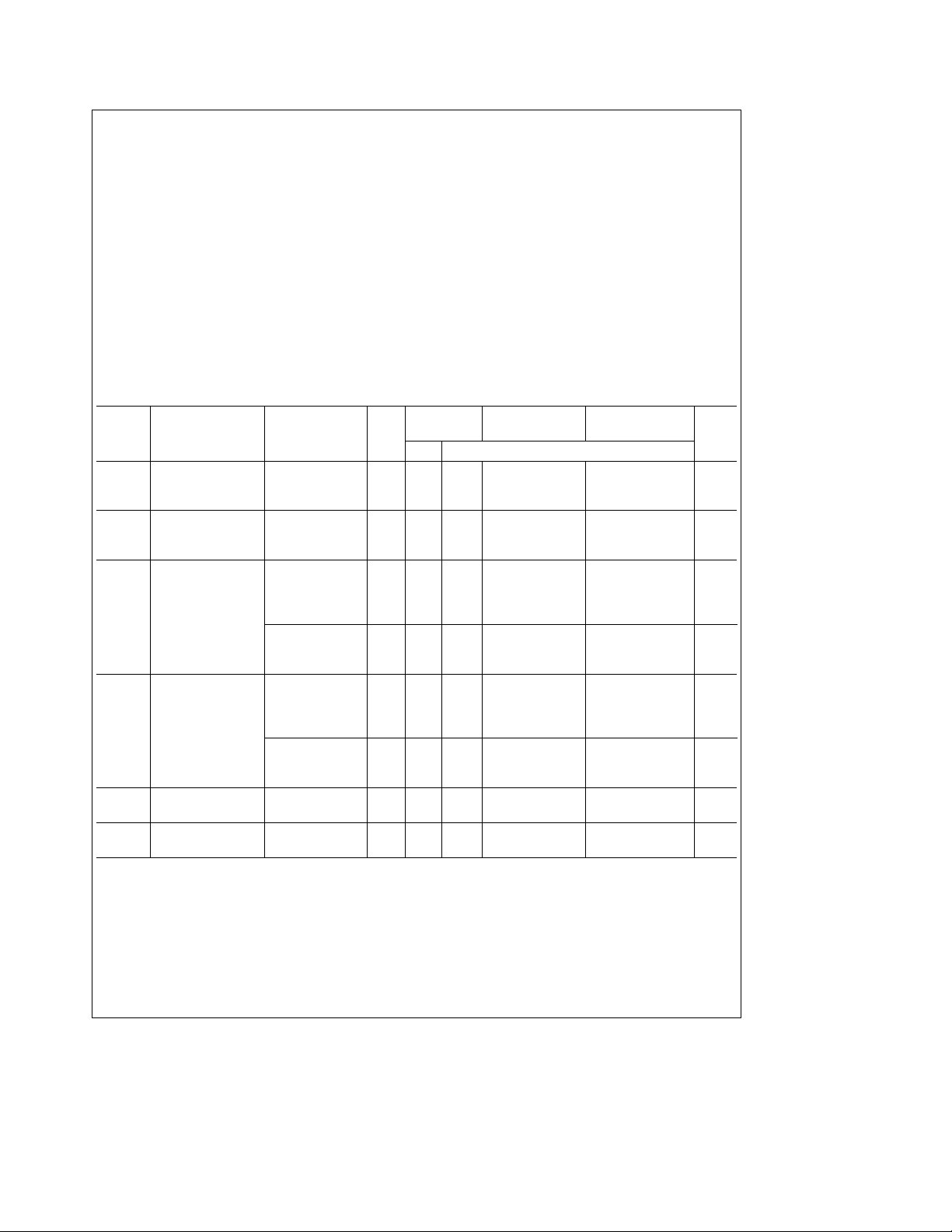
DC Electrical Characteristics (Note 4)
Symbol Parameter Conditions V
CC
A
e
T
25§C
Typ Guaranteed Limits
V
IH
Minimum High Level 2.0V 1.5 1.5 1.5 V
Input Voltage 4.5V 3.15 3.15 3.15 V
6.0V 4.2 4.2 4.2 V
V
IL
Maximum Low Level 2.0V 0.5 0.5 0.5 V
Input Voltage** 4.5V 1.35 1.35 1.35 V
6.0V 1.8 1.8 1.8 V
V
OH
Minimum High Level V
Output Voltage
e
VIHor V
l
IN
I
OUT
IL
s
20 mA 2.0V 2.0 1.9 1.9 1.9 V
l
4.5V 4.5 4.4 4.4 4.4 V
6.0V 6.0 5.9 5.9 5.9 V
e
V
VIHor V
IN
I
l
OUT
I
l
OUT
l
IN
I
OUT
e
V
OL
Maximum Low Level V
Output Voltage
IL
s
4.0 mA 4.5V 4.2 3.98 3.84 3.7 V
l
s
5.2 mA 6.0V 5.7 5.48 5.34 5.2 V
l
VIHor V
IL
s
20 mA 2.0V 0 0.1 0.1 0.1 V
l
4.5V 0 0.1 0.1 0.1 V
6.0V 0 0.1 0.1 0.1 V
e
V
VIHor V
IN
I
l
OUT
I
l
OUT
I
IN
I
CC
Note 1: Absolute Maximum Ratings are those values beyond which damage to the device may occur.
Note 2: Unless otherwise specified all voltages are referenced to ground.
Note 3: Power Dissipation temperature derating Ð plastic ‘‘N’’ package:
Note 4: For a power supply of 5V
with this supply. Worst case V
I
**V
Maximum Input V
Current
Maximum Quiescent V
Supply Current I
g
and VILoccur at V
) occur for CMOS at the higher voltage and so the 6.0V values should be used.
OZ
limits are currently tested at 20% of VCC. The above VILspecification (30% of VCC) will be implemented no later than Q1, CY’89.
IL
IH
e
IN
e
IN
OUT
10% the worst case output voltages (VOH, and VOL) occur for HC at 4.5V. Thus the 4.5V values should be used when designing
IL
s
4.0 mA 4.5V 0.2 0.26 0.33 0.4 V
l
s
5.2 mA 6.0V 0.2 0.26 0.33 0.4 V
l
VCCor GND 6.0V
g
0.1
VCCor GND 6.0V 8.0 80 160 mA
e
0 mA
b
12 mW/§C from 65§Cto85§C; ceramic ‘‘J’’ package:b12 mW/§C from 100§Cto125§C.
e
5.5V and 4.5V respectively. (The VIHvalue at 5.5V is 3.85V.) The worst case leakage current (IIN,ICC, and
CC
74HC 54HC
eb
T
40 to 85§CT
A
g
1.0
Min Max Units
V
§
§
Units
b
b
40
55
eb
A
55 to 125§C
g
CC
a
85
a
125
1.0 mA
C
C
2
Page 3
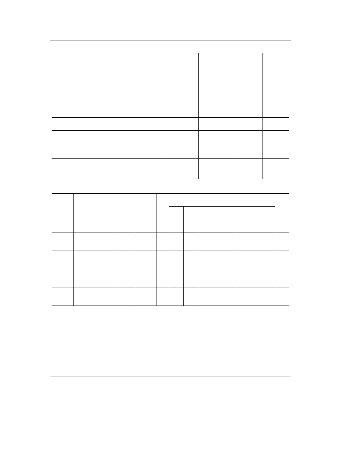
AC Electrical Characteristics T
Symbol Parameter
f
MAX
t
PLH,tPHL
t
PLH,tPHL
t
PLH,tPHL
t
PLH,tPHL
t
PLH,tPHL
t
PLH,tPHL
t
PLH,tPHL
t
PHL,tPLH
t
W
Maximum Clock 40 MHz
Frequency
Maximum Propagation Delay Time Load QA,Q
Maximum Propagation Delay Time Data A, QA,Q
Maximum Propagation Delay Time Clock Ripple 16 ns
Maximum Propagation Delay Time Clock QA,Q
Maximum Propagation Delay Time Clock Max/Min 30 ns
Maximum Propagation Delay Time Down/Up Ripple 29 ns
Maximum Propagation Delay Time Down/Up Max/Min 22 ns
Maximum Propagation Delay Time Enable Ripple Clock 22 ns
Minimum Clock, Clear or Load 10 ns
Input Pulse Width
A
e
25§C, V
e
e
CC
5.0V, t
e
t
6 ns, C
r
f
From To
(Input) (Output)
B, C, D Q
e
15 pF (unless otherwise specified)
L
Typ Units
Q
B
C,QD
B
C,QD
30 ns
27 ns
Clock
Q
B
C,QD
24 ns
Clock
AC Electrical Characteristics V
Symbol Parameter
f
MAX
t
PLH,tPHL
t
PLH,tPHL
t
PLH,tPHL
t
PLH,tPHL
Maximum Clock 2.0V 9 4.0 3.5 2.6 MHz
Frequency 4.5V 30 20 16 13 MHz
Maximum Propagation Load QA,QB2.0V 80 220 275 330 ns
Delay Time Q
Maximum Propagation Data A, QA,QB2.0V 71 200 250 300 ns
Delay Time B, C, D Q
Maximum Propagation Clock Ripple 2.0V 44 125 155 190 ns
Delay Time Clock 4.5V 25 25 31 38 ns
Maximum Propagation Clock QA,QB2.0V 83 215 270 325 ns
Delay Time QC,QD4.5V 29 43 54 65 ns
From To T
(Input) (Output)
e
2.0V to 6.0V, C
CC
V
CC
e
L
e
25§C
A
50 pF, t
e
e
t
6 ns (unless otherwise specified)
r
f
74HC 54HC
eb
T
40 to 85§CT
A
A
eb
Typ Guaranteed Limits
6.0V 36 24 19 15 MHz
4.5V 27 44 55 66 ns
C,QD
6.0V 21 37 47 56 ns
4.5V 25 40 50 60 ns
C,QD
6.0V 19 34 43 51 ns
6.0V 14 21 26 32 ns
6.0V 22 37 46 55 ns
55 to 125§C Units
3
Page 4

AC Electrical Characteristics (Continued)
e
T
Symbol Parameter
From To
(Input) (Output)
Conditions V
CC
25§C
A
Typ Guaranteed Limits
t
PLH,tPHL
Maximum Propagation Clock Max/Min 2.0V 125 255 320 385 ns
Delay Time 4.5V 41 51 64 77 ns
6.0V 31 43 54 65 ns
t
PLH,tPHL
Maximum Propagation Down/Up Ripple 2.0V 90 210 265 315 ns
Delay Time Clock 4.5V 30 42 53 63 ns
6.0V 24 36 45 54 ns
t
PLH,tPHL
Maximum Propagation Down/Up Max/Min 2.0V 88 190 240 285 ns
Delay Time 4.5V 30 38 48 57 ns
6.0V 23 32 41 48 ns
t
PHL,tPLH
Maximum Propagation Enable Ripple 2.0V 50 125 155 190 ns
Delay Time Clock 4.5V 18 25 31 38 ns
6.0V 14 21 26 32 ns
t
W
Minimum Clock, Load or 2.0V 36 125 155 190 ns
Clear Input Pulse Width 4.5V 12 25 31 38 ns
6.0V 9 21 26 32 ns
t
S
Minimum Setup Time Data Load 2.0V 50 100 125 150 ns
4.5V 14 20 25 30 ns
6.0V 10 17 21 26 ns
t
H
Data Hold Time Load Data 2.0Vb16 25 30 40 ns
b
4.5V
35 6 8 ns
6.0Vb25 6 7 ns
tSMinimum Setup Time Down/Up Clock 2.0V 62 150 190 225 ns
4.5V 18 30 38 48 ns
6.0V 14 26 33 38 ns
t
H
Minimum Hold Time Clock Down/Up 2.0Vb23 0 0 0 ns
4.5Vb50 0 0 ns
b
6.0V
40 0 0 ns
tSMinimum Setup Time Enable Clock 2.0V 28 100 125 150 ns
4.5V 10 20 25 30 ns
6.0V 7 17 21 26 ns
t
H
Minimum Hold Time Clock Enable 2.0Vb11 0 0 0 ns
b
4.5V
50 0 0 ns
6.0Vb30 0 0 ns
t
rem
Minimum Removal Time Load Clock 2.0V 1 25 30 40 ns
4.5V 1 5 6 8 ns
6.0V 0 5 6 7 ns
t
THL,tTLH
Maximum Output 2.0V 30 75 95 110 s
Rise and Fall Time 4.5V 10 15 19 22 ns
6.0V 9 13 16 19 ns
t
W
Minimum Load 2.0V 53 100 125 150 ns
Pulse Width 4.5V 15 20 25 30 ns
6.0V 12 17 21 26 ns
C
C
Input Capacitance 5 10 10 10 pF
IN
Power Dissipation 35 pF
PD
Capacitance (Note 5)
Note 5: CPDdetermines the no load dynamic power consumption, P
ICC.
D
e
2
CPDV
faICCVCC, and the no load dynamic current consumption, I
CC
74HC 54HC
eb
40 to 85§CT
T
A
A
eb
55 to 125§C
e
CPDVCCf
S
Units
a
4
Page 5

Logic Diagrams
’HC190 Decade Counters
Pin (16)eVCC, Pin (8)eGND
TL/F/5322– 2
5
Page 6

Logic Diagrams (Continued)
’HC191 Binary Counters
Pin (16)eVCC, Pin (8)eGND
6
TL/F/5322– 3
Page 7

Timing Diagrams
’HC190 Synchronous Decade Counters
Typical Load, Count, and Inhibit Sequences
Sequence:
(1) Load (preset) to BCD seven
(2) Count up to eight, nine, zero, one and two
(3) Inhibit
(4) Count down to one, zero, nine, eight, and seven
’HC191 Synchronous Binary Counters
Typical Load, Count, and Inhibit Sequence
Sequence:
(1) Load (preset) to binary thirteen
(2) Count up to fourteen, fifteen, zero, one, and two
(3) Inhibit
(4) Count down to one, zero, fifteen, fourteen, and thirteen
7
TL/F/5322– 4
TL/F/5322– 5
Page 8
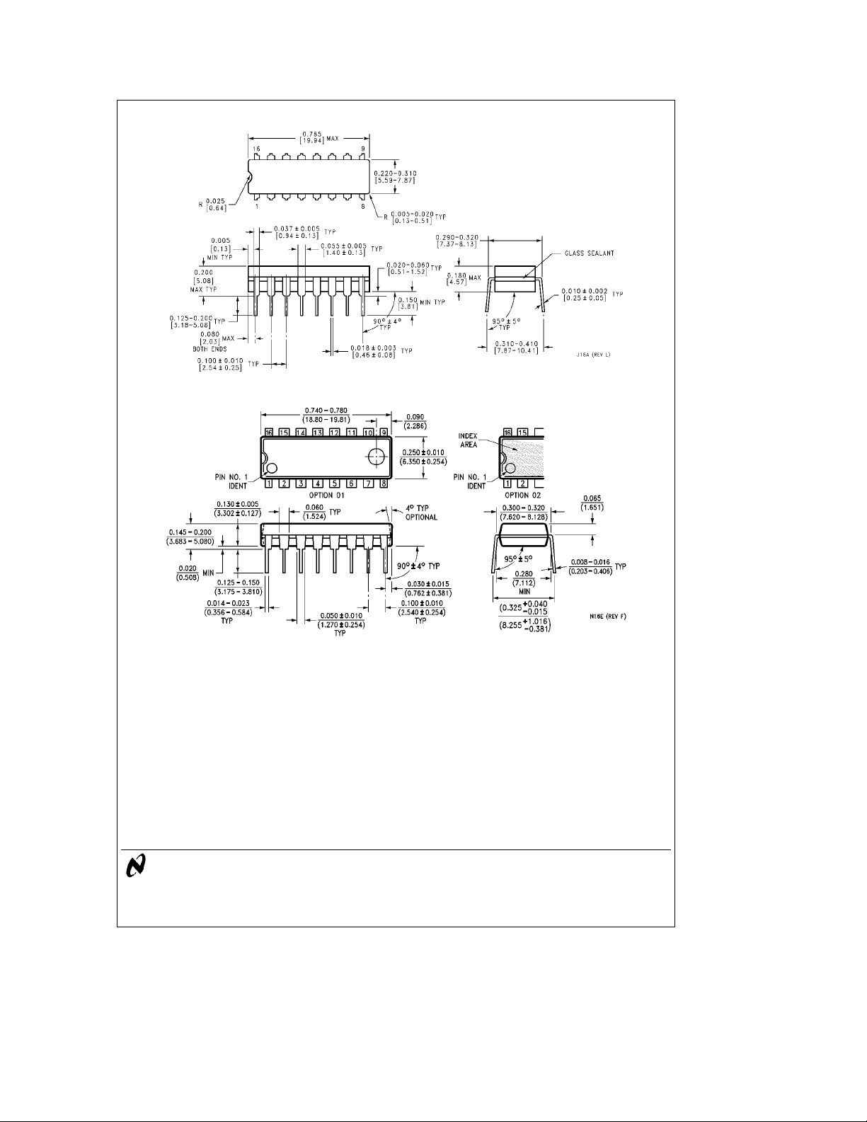
Physical Dimensions inches (millimeters)
Order Number MM54HC190J, MM54HC191J, MM74HC190J, or MM74HC191J
NS Package J16A
MM54HC190/MM74HC190/MM54HC191/MM74HC191
Order Number MM74HC190N or MM74HC191N
LIFE SUPPORT POLICY
NATIONAL’S PRODUCTS ARE NOT AUTHORIZED FOR USE AS CRITICAL COMPONENTS IN LIFE SUPPORT
DEVICES OR SYSTEMS WITHOUT THE EXPRESS WRITTEN APPROVAL OF THE PRESIDENT OF NATIONAL
SEMICONDUCTOR CORPORATION. As used herein:
1. Life support devices or systems are devices or 2. A critical component is any component of a life
systems which, (a) are intended for surgical implant support device or system whose failure to perform can
into the body, or (b) support or sustain life, and whose be reasonably expected to cause the failure of the life
failure to perform, when properly used in accordance support device or system, or to affect its safety or
with instructions for use provided in the labeling, can effectiveness.
be reasonably expected to result in a significant injury
to the user.
NS Package N16E
National Semiconductor National Semiconductor National Semiconductor National Semiconductor
Corporation Europe Hong Kong Ltd. Japan Ltd.
1111 West Bardin Road Fax: (
Arlington, TX 76017 Email: cnjwge@tevm2.nsc.com Ocean Centre, 5 Canton Rd. Fax: 81-043-299-2408
Tel: 1(800) 272-9959 Deutsch Tel: (
Fax: 1(800) 737-7018 English Tel: (
National does not assume any responsibility for use of any circuitry described, no circuit patent licenses are implied and National reserves the right at any time without notice to change said circuitry and specifications.
Fran3ais Tel: (
Italiano Tel: (
a
49) 0-180-530 85 86 13th Floor, Straight Block, Tel: 81-043-299-2309
a
49) 0-180-530 85 85 Tsimshatsui, Kowloon
a
49) 0-180-532 78 32 Hong Kong
a
49) 0-180-532 93 58 Tel: (852) 2737-1600
a
49) 0-180-534 16 80 Fax: (852) 2736-9960
 Loading...