

Page 1
MM54HC166/MM74HC166
8-Bit Parallel In/Serial Out Shift Registers
General Description
The MM54HC166/MM74HC166 high speed 8-BIT PARALLEL-IN/SERIAL-OUT SHIFT REGISTER utilizes advanced
silicon-gate CMOS technology. It has low power consumption and high noise immunity of standard CMOS integrated
circuits, along with the ability to drive 10 LS-TTL loads.
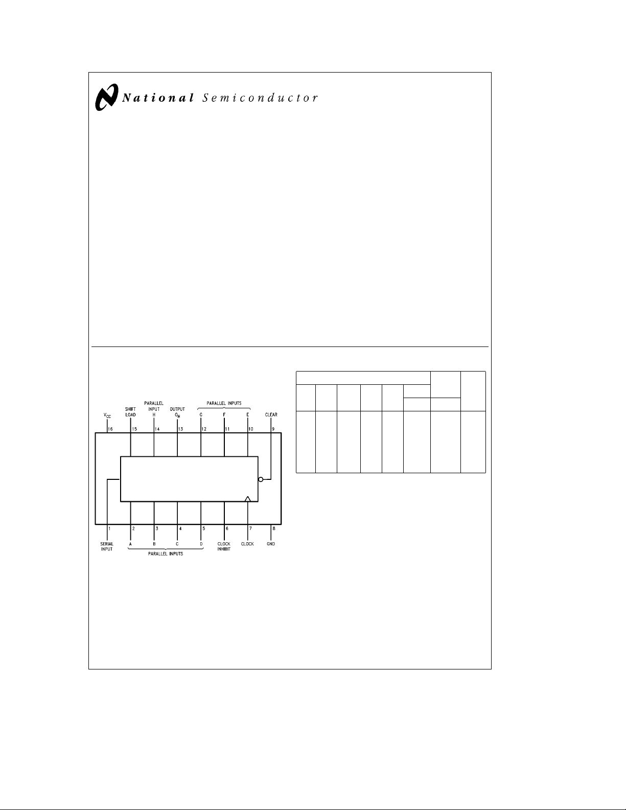
These Parallel-In or Serial-In, Serial-Out shift registers feature gated CLOCK inputs and an overriding CLEAR input.
The load mode is established by the SHIFT/LOAD input.
When high, this input enables the SERIAL INPUT and couples the eight flip-flops for serial shifting with each clock
pulse. When low, the PARALLEL INPUTS are enabled and
synchronous loading occurs on the next clock pulse. During
parallel loading, serial data flow is inhibited. Clocking is accomplished on the low-to-high level edge of the CLOCK
pulse through a 2-input NOR gate, permitting one input to
be used as a clock enable or CLOCK INHIBIT function.
Holding either of the clock inputs high inhibits clocking;
holding either low enables the other clock input. This allows
the system clock to be free running, and the register can be
stopped on command with the other clock input. The
CLOCK INHIBIT input should be changed to the high level
only while the clock input is high. A direct CLEAR input overrides all other inputs, including the CLOCK, and sets all flipflops to zero.
The 54HC/74HC logic family is functionally as well as pin
out compatible with the standard 54LS/74LS logic family.
All inputs are protected from damage due to static discharge by internal diode clamps to V
Features
Y
Typical propagation delay:
Y
Wide operating supply voltage range: 2V –6V
Y
Low input current:k1 mA
Y
Low quiescent supply current: 80 mA maximum
(74HC Series)
Y
Fanout of 10 LS-TTL loads
and Ground.
CC
MM54HC166/MM74HC166 8-Bit Parallel In/Serial Out Shift Registers
August 1989
Connection Diagram
Dual-In-Line Package
Order Number MM54HC166 or MM74HC166
TL/F/5770– 1
Function Table
Inputs Internal
Clear
Shift/ Clock
Load Inhibit
Clock Serial
Parallel
A...H Q
LX X XX XLLL
HX L L X XQ
HL L
HH L
HH L
HX H
HeHigh Level (steady state), LeLow Level (steady state)
e
X
Don’t Care (any input, including transitions)
e
Transition from low to high level
u
e
a...h
The level of steady-state input at inputs A through H, respectively
Q
A0,QB0,QH0
steady-state input conditions were established
Q
An,QGn
transition of the clock
e
The level of QA,QB,QH, respectively, before the indicated
e
The level of QA,QG, respectively, before the most recent
X a...h a b h
u
HXHQAnQ
u
LXLQAnQ
u
XXQA0QB0Q
u
Output
Outputs
AQB
A0QB0QH0
Q
H
Gn
Gn
H0
u
C
1995 National Semiconductor Corporation RRD-B30M105/Printed in U. S. A.
TL/F/5770
Page 2
Absolute Maximum Ratings (Notes1&2)
Operating Conditions
If Military/Aerospace specified devices are required,
please contact the National Semiconductor Sales
Office/Distributors for availability and specifications.
Supply Voltage (V
CC
)
DC Input Voltage (VIN)
DC Output Voltage (V
OUT
)
Clamp Diode Current (IIK,IOK)
DC Output Current, per Pin (I
OUT
)
DC VCCor GND Current, per Pin (ICC)
Storage Temperature Range (T
STG
b
b
)
b
0.5V toa7.0V
1.5V to V
CC
0.5V to V
CC
g
g
b
g
65§Ctoa150§C
a
1.5V
a
0.5V
20 mA
25 mA
50 mA
Power Dissipation (PD)
Supply Voltage (V
DC Input or Output Voltage
(V
IN,VOUT
Operating Temp. Range (T
)26V
CC
)0V
MM74HC
MM54HC
Input Rise or Fall Times (t
e
V
2.0V 1000 ns
CC
e
V
4.5V 500 ns
CC
e
V
6.0V 400 ns
CC
(Note 3) 600 mW
S.O. Package only 500 mW
Lead Temperature (T
(Soldering, 10 seconds) 260
)
L
C
§
DC Electrical Characteristics (Note 4)
Symbol Parameter Conditions V
CC
A
e
T
25§C
Typ Guaranteed Limits
V
Minimum High 2.0V 1.5 1.5 1.5 V
IH
Level Input 4.5V 3.15 3.15 3.15 V
Voltage 6.0V 4.2 4.2 4.2 V
V
Maximum Low 2.0V 0.5 0.5 0.5 V
IL
Level Input 4.5V 1.35 1.35 1.35 V
Voltage** 6.0V 1.8 1.8 1.8 V
V
OH
Minimum High V
Level OutputlI
Voltage 4.5V 4.5 4.4 4.4 4.4 V
e
VIHor V
IN
OUT
IL
s
20 mA 2.0V 2.0 1.9 1.9 1.9 V
l
6.0V 6.0 5.9 5.9 5.9 V
e
V
VIHor V
IN
I
l
OUT
I
l
OUT
V
OL
Maximum Low V
Level OutputlI
Voltage 4.5V 0 0.1 0.1 0.1 V
IN
OUT
e
IL
s
4.0 mA 4.5V 4.2 3.98 3.84 3.7 V
l
s
5.2 mA 6.0V 5.7 5.48 5.34 5.2 V
l
VIHor V
IL
s
20 mA 2.0V 0 0.1 0.1 0.1 V
l
6.0V 0 0.1 0.1 0.1 V
e
V
VIHor V
IN
I
l
OUT
I
l
OUT
I
IN
I
CC
Maximum V
Input Current V
Maximum V
Quiescent I
Supply Current V
Note 1: Absolute Maximum ratings are those values beyond which damage to the device may occur.
Note 2: Unless otherwise specified all voltages are referenced to ground.
Note 3: Power dissipation temperature deratingÐplastic ‘‘N’’ package:
Note 4: For a power supply of 5V
designing with this supply. Worst-case V
, and IOZ) occur for CMOS at the higher voltage and so the 6.0V values should be used.
(I
IN,ICC
**V
limits are currently tested at 20% of VCC. The above VILspecification (30% of VCC) will be implemented no later than Q1, CY’89.
IL
e
IN
CC
e
IN
OUT
CC
g
10%, the worst-case output voltages (VOHand VOL) occur for HC at 4.5V. Thus, the 4.5V values should be used when
IL
s
4.0 mA 4.5V 0.2 0.26 0.33 0.4 V
l
s
5.2 mA 6.0V 0.2 0.26 0.33 0.4 V
l
VCCor GND
e
2V–6V
6.0V
g
0.1
VCCor GND
e
0 mA 6.0V 8.0 80 160 mA
e
2V–6V
b
12 mW/§C from 65§Cto85§C; ceramic ‘‘J’’ package:b12 mW/§C from 100§Cto125§C.
and VILoccur at V
IH
e
5.5V and 4.5V, respectively. (The VIHvalue at 5.5V is 3.85V.) The worst-case leakage current
CC
74HC 54HC
eb
T
40§Ctoa85§CT
A
g
1.0
Min Max Units
)
A
b
40
b
55
)
r,tf
eb
55§Ctoa125§C
A
g
CC
a
85
a
125
V
C
§
C
§
Units
1.0 mA
2
Page 3

AC Electrical Characteristics C
Symbol Parameter V
CC
e
L
T
A
50 pF, t
e
25§C
e
e
t
6 ns unless otherwise noted
r
f
74HC 54HC
eb
T
40§Ctoa85§CT
A
eb
55§Ctoa125§C
A
Typ Guaranteed Limits
f
MAX
t
PHL
t
PLH
t
PHL
t
PLH
t
su
t
su
t
REM
t
h
tr,t
t
w
C
C
pd
in
Maximum 2.0V 6 5 4.2 MHz
Operating Frequency 4.5V 31 25 21 MHz
/ Maximum Propagation 2.0V 140 175 210 ns
Delay Clock to Q
/ Maximum Propagation 2.0V 130 165 195 ns
Delay Clear to Q
Minimum Setup Time 2.0V 80 100 120 ns
Shift/Load to Clock 4.5V 16 20 24 ns
Minimum Setup Time 2.0V 80 100 120 ns
Data before Clock 4.5V 16 20 24 ns
Minimum Removal 2.0V 0 0 0 ns
Time Clear to Clock 4.5V 0 0 0 ns
Maximum Hold Time 2.0V 0 0 0 ns
Data after Clock 4.5V 0 0 0 ns
Maximum Output 2.0V 75 95 110 ns
f
Rise and Fall Time 4.5V 7 15 19 22 ns
Minimum Pulse 2.0V 80 100 120 ns
Width Clock or Clear 4.5V 16 20 24 ns
Power Dissipation (per
Capacitance (Note 5) package)
Maximum Input
Capacitance
H
h
6.0V 36 29 25 MHz
4.5V 14 28 35 42 ns
6.0V 24 30 36 ns
4.5V 11 26 35 39 ns
6.0V 22 30 33 ns
6.0V 14 18 20 ns
6.0V 14 18 20 ns
6.0V 0 0 0 ns
6.0V 0 0 0 ns
6.0V 13 16 19 ns
6.0V 14 16 20 ns
100 pF
510 10 10 pF
Units
AC Electrical Characteristics V
CC
5V, C
L
e
15 pF, T
e
A
25§C, t
e
e
t
6 ns unless otherwise noted
r
f
e
Symbol Parameter Typical Guaranteed Limits Units
f
MAX
t
/ Maximum Propagation
PHL
t
PLH
t
/ Maximum Propagation
PHL
t
PLH
t
su
t
su
t
REM
t
h
t
w
Note 5: Cpddetermines the no load dynamic power consumption, P
ICC.
Maximum
Operating Frequency
Delay Clock to Q
Delay Clear to Q
Minimum Setup Time
Shift/Load High 16
to Clock
Minimum Setup Time
Data before Clock
Minimum Removal Time
Clear to Clock
Maximum Hold Time
Data after Clock
Minimum Pulse
Width Clock or Clear
h
h
2
e
D
CPDV
a
f
ICCVCC, and the no load dynamic current consumption, I
CC
31 MHz
16 ns
12 ns
16 ns
0ns
0ns
16 ns
S
3
e
CPDV
ns
a
f
CC
Page 4

Logic Diagram
TL/F/5770– 2
4
Page 5

Logic Diagram
Typical Clear, Shift, Load, Inhibit and Shift Sequences
TL/F/5770– 3
5
Page 6

Physical Dimensions inches (millimeters)
Order Number MM54HC166 or MM74HC166
NS Package Number M16A
Order Number MM54HC166 or MM74HC166
NS Package Number N16E
MM54HC166/MM74HC166 8-Bit Parallel In/Serial Out Shift Registers
LIFE SUPPORT POLICY
NATIONAL’S PRODUCTS ARE NOT AUTHORIZED FOR USE AS CRITICAL COMPONENTS IN LIFE SUPPORT
DEVICES OR SYSTEMS WITHOUT THE EXPRESS WRITTEN APPROVAL OF THE PRESIDENT OF NATIONAL
SEMICONDUCTOR CORPORATION. As used herein:
1. Life support devices or systems are devices or 2. A critical component is any component of a life
systems which, (a) are intended for surgical implant support device or system whose failure to perform can
into the body, or (b) support or sustain life, and whose be reasonably expected to cause the failure of the life
failure to perform, when properly used in accordance support device or system, or to affect its safety or
with instructions for use provided in the labeling, can effectiveness.
be reasonably expected to result in a significant injury
to the user.
National Semiconductor National Semiconductor National Semiconductor National Semiconductor
Corporation Europe Hong Kong Ltd. Japan Ltd.
1111 West Bardin Road Fax: (
Arlington, TX 76017 Email: cnjwge@tevm2.nsc.com Ocean Centre, 5 Canton Rd. Fax: 81-043-299-2408
Tel: 1(800) 272-9959 Deutsch Tel: (
Fax: 1(800) 737-7018 English Tel: (
National does not assume any responsibility for use of any circuitry described, no circuit patent licenses are implied and National reserves the right at any time without notice to change said circuitry and specifications.
Fran3ais Tel: (
Italiano Tel: (
a
49) 0-180-530 85 86 13th Floor, Straight Block, Tel: 81-043-299-2309
a
49) 0-180-530 85 85 Tsimshatsui, Kowloon
a
49) 0-180-532 78 32 Hong Kong
a
49) 0-180-532 93 58 Tel: (852) 2737-1600
a
49) 0-180-534 16 80 Fax: (852) 2736-9960
 Loading...