

National Semiconductor MM54HC139, MM74HC139 Service Manual
MM54HC139/MM74HC139
Dual 2-To-4 Line Decoder
General Description
This decoder utilizes advanced silicon-gate CMOS technology, and is well suited to memory address decoding or data
routing applications. It possesses the high noise immunity
and low power consumption usually associated with CMOS
circuitry, yet has speeds comparable to low power Schottky
TTL logic.
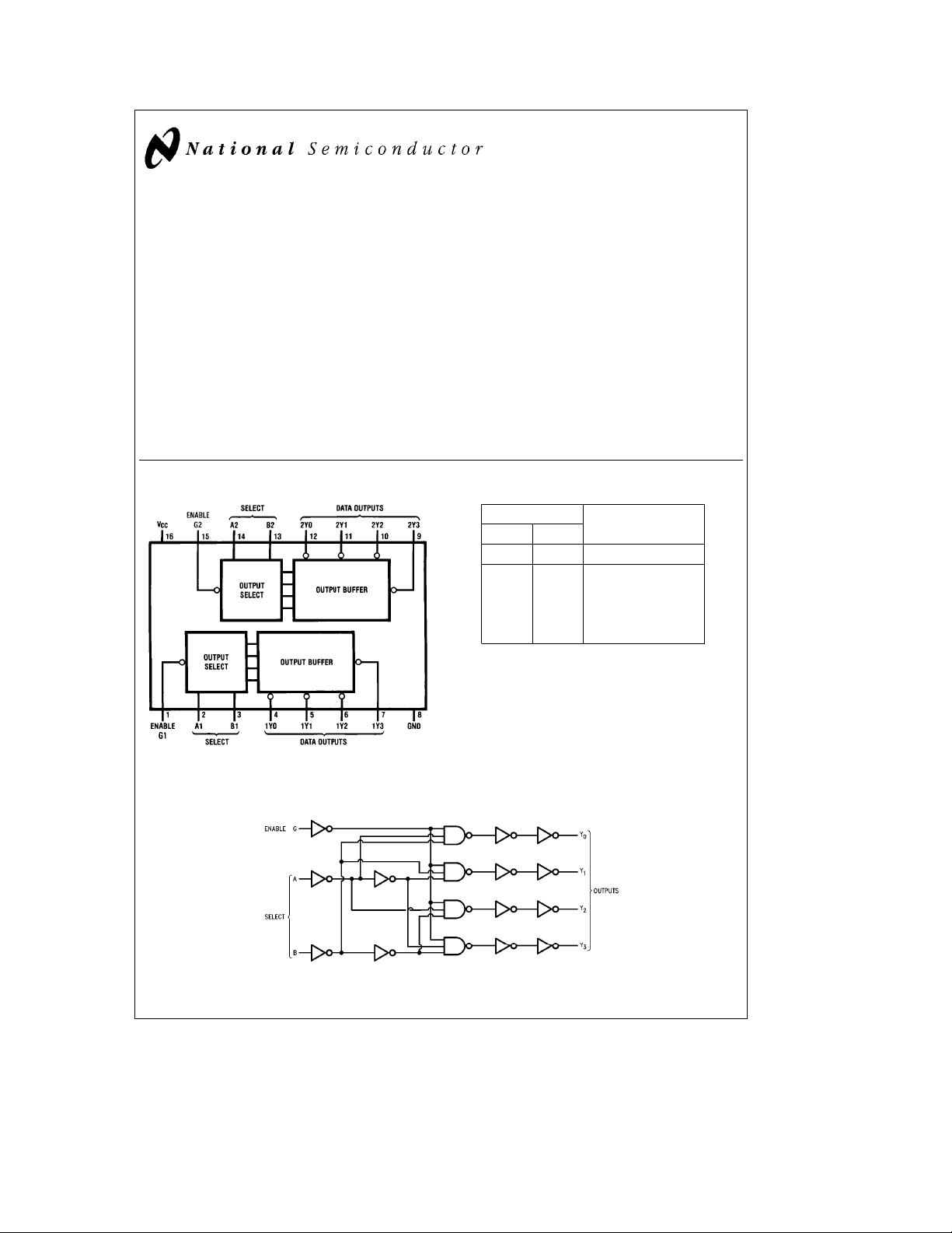
The MM54HC139/MM74HC139 contain two independent
one-of-four decoders each with a single active low enable
input (G1, or G2). Data on the select inputs (A1, and B1 or
A2, and B2) cause one of the four normally high outputs to
go low.
The decoder’s outputs can drive 10 low power Schottky TTL
equivalent loads, and are functionally as well as pin equiva-
January 1988
lent to the 54LS139/74LS139. All inputs are protected from
damage due to static discharge by diodes to V
ground.
CC
and
Features
Y
Typical propagation delays Ð
Select to outputs (4 delays): 18 ns
Select to output (5 delays): 28 ns
Enable to output: 20 ns
Y
Low power: 40 mW quiescent supply power
Y
Fanout of 10 LS-TTL devices
Y
Input current maximum 1 mA, typical 10 pA
MM54HC139/MM74HC139 Dual 2-To-4 Line Decoder
Connection Diagram
Dual-In-Line Package
Order Number MM54HC139 or MM74HC139
Logic Diagram
Truth Table
Enable Select
Hehigh level, Lelow level, Xedon’t care
TL/F/5311– 1
MM54HC139/MM74HC139
’HC139
Inputs
G BAY0Y1Y2Y3
H XXHHHH
L LLLHHH
L LHHLHH
L HLHHLH
L HHHHHL
Outputs
(1of2)
C
1995 National Semiconductor Corporation RRD-B30M105/Printed in U. S. A.
TL/F/5311
TL/F/5311– 2
Absolute Maximum Ratings (Notes1&2)
Operating Conditions
If Military/Aerospace specified devices are required,
please contact the National Semiconductor Sales
Office/Distributors for availability and specifications.
Supply Voltage (V
CC
)
DC Input Voltage (VIN)
DC Output Voltage (V
OUT
)
Clamp Diode Current (IIK,IOK)
DC Output Current, per pin (I
OUT
)
DC VCCor GND Current, per pin (ICC)
Storage Temperature Range (T
STG
b
b
)
b
0.5 toa7.0V
1.5 to V
CC
0.5 to V
CC
g
g
b
g
65§Ctoa150§C
a
1.5V
a
0.5V
20 mA
25 mA
50 mA
Supply Voltage (V
)26V
CC
DC Input or Output Voltage 0 V
(V
IN,VOUT
)
Operating Temp. Range (TA)
MM74HC
MM54HC
Input Rise or Fall Times
e
V
2.0V(tr,tf) 1000 ns
CC
e
V
4.5V 500 ns
CC
e
V
6.0V 400 ns
CC
Power Dissipation (PD)
(Note 3) 600 mW
S.O. Package only 500 mW
Lead Temp. (T
) (Soldering 10 seconds) 260§C
L
DC Electrical Characteristics (Note 4)
Symbol Parameter Conditions V
CC
A
e
T
25§C
Typ Guaranteed Limits
V
IH
Minimum High Level 2.0V 1.5 1.5 1.5 V
Input Voltage 4.5V 3.15 3.15 3.15 V
6.0V 4.2 4.2 4.2 V
V
IL
Maximum Low Level 2.0V 0.5 0.5 0.5 V
Input Voltage** 4.5V 1.35 1.35 1.35 V
6.0V 1.8 1.8 1.8 V
V
OH
Minimum High Level V
Output Voltage
e
VIHor V
l
I
IN
OUT
IL
s
20 mA 2.0V 2.0 1.9 1.9 1.9 V
l
4.5V 4.5 4.4 4.4 4.4 V
6.0V 6.0 5.9 5.9 5.9 V
e
V
VIHor V
IN
I
l
OUT
I
l
OUT
l
I
IN
OUT
e
V
OL
Maximum Low Level V
Output Voltage
IL
s
4.0 mA 4.5V 4.2 3.98 3.84 3.7 V
l
s
5.2 mA 6.0V 5.7 5.48 5.34 5.2 V
l
VIHor V
IL
s
20 mA 2.0V 0 0.1 0.1 0.1 V
l
4.5V 0 0.1 0.1 0.1 V
6.0V 0 0.1 0.1 0.1 V
e
V
VIHor V
IN
I
l
OUT
I
l
OUT
I
IN
I
CC
Note 1: Absolute Maximum Ratings are those values beyond which damage to the device may occur.
Note 2: Unless otherwise specified all voltages are referenced to ground.
Note 3: Power Dissipation temperature derating Ð plastic ‘‘N’’ package:
Note 4: For a power supply of 5V
with this supply. Worst case V
I
**V
Maximum Input V
Current
Maximum Quiescent V
Supply Current I
g
and VILoccur at V
) occur for CMOS at the higher voltage and so the 6.0V values should be used.
OZ
limits are currently tested at 20% of VCC. The above VILspecification (30% of VCC) will be implemented no later than Q1, CY’89.
IL
IH
e
IN
e
IN
OUT
10% the worst case output voltages (VOH, and VOL) occur for HC at 4.5V. Thus the 4.5V values should be used when designing
IL
s
4.0 mA 4.5V 0.2 0.26 0.33 0.4 V
l
s
5.2 mA 6.0V 0.2 0.26 0.33 0.4 V
l
VCCor GND 6.0V
g
0.1
VCCor GND 6.0V 8.0 80 160 mA
e
0 mA
b
12 mW/§C from 65§Cto85§C; ceramic ‘‘J’’ package:b12 mW/§C from 100§Cto125§C.
e
5.5V and 4.5V respectively. (The VIHvalue at 5.5V is 3.85V.) The worst case leakage current (IIN,ICC, and
CC
74HC 54HC
eb
T
40 to 85§CT
A
g
1.0
Min Max Units
V
§
§
Units
b
40
b
55
eb
A
CC
a
85
a
125
55 to 125§C
g
1.0 mA
C
C
2
 Loading...