

National Semiconductor MM54HC137, MM74HC137 Service Manual
MM54HC137/MM74HC137 3-to-8 Line
Decoder With Address Latches
(Inverted Output)
General Description
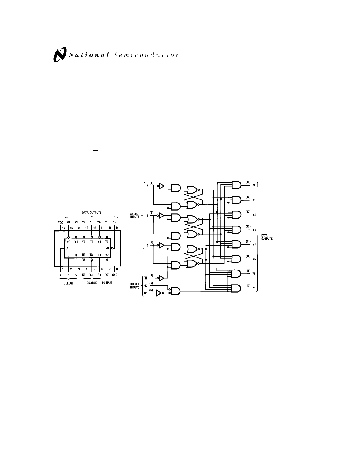
This device utilizes advanced silicon-gate CMOS technology, to implement a three-to-eight line decoder with latches
on the three address inputs. When GL
high, the address present at the select inputs (A, B and C) is
stored in the latches. As long as GL
dress changes will be recognized. Output enable controls,
G1 and G2
the select or latch-enable inputs. All of the outputs are high
unless G1 is high and G2
for the implementation of glitch-free decoders in stored-address applications in bus oriented systems.
, control the state of the outputs independently of
is low. The HC137 is ideally suited
goes from low to
remains high no ad-
Connection and Functional Block Diagrams
Dual-In-Line Package
The 54HC/74HC logic family is speed, function and pin-out
compatible with the standard 54LS/74LS logic family. All
inputs are protected from damage due to static discharge by
diodes to V
CC
Features
Y
Typical propagation delay: 20 ns
Y
Wide supply range: 2– 6V
Y
Latched inputs for easy interfacing.
Y
Fanout of 10 LS-TTL loads.
and ground.
November 1995
MM54HC137/MM74HC137 3-to-8 Line
Decoder With Address Latches (Inverted Output)
TL/F/5310– 1
Order Number MM54HC137
or MM74HC137
C
1995 National Semiconductor Corporation RRD-B30M115/Printed in U. S. A.
TL/F/5310
TL/F/5310– 2
Absolute Maximum Ratings (Notes1&2)
If Military/Aerospace specified devices are required,
please contact the National Semiconductor Sales
Office/Distributors for availability and specifications.
Supply Voltage (V
CC
)
DC Input Voltage (VIN)
DC Output Voltage (V
OUT
)
Clamp Diode Current (IIK,IOK)
DC Output Current, per pin (I
OUT
)
DC VCCor GND Current, per pin (ICC)
Storage Temperature Range (T
STG
b
b
)
b
0.5 toa7.0V
1.5 to V
CC
0.5 to V
CC
g
g
b
g
65§Ctoa150§C
a
1.5V
a
0.5V
20 mA
25 mA
50 mA
Operating Conditions
Supply Voltage (V
DC Input or Output Voltage 0 V
(V
IN,VOUT
Operating Temp. Range (T
MM74HC
MM54HC
Input Rise or Fall Times
)26V
CC
)
e
2.0V(tr,tf) 1000 ns
V
CC
e
4.5V 500 ns
V
CC
e
6.0V 400 ns
V
CC
Power Dissipation (PD)
(Note 3) 600 mW
S.O. Package only 500 mW
Lead Temperature (T
)
L
(Soldering 10 seconds) 260§C
DC Electrical Characteristics (Note 4)
Symbol Parameter Conditions V
CC
A
e
T
25§C
Typ Guaranteed Limits
V
IH
Minimum High Level 2.0V 1.5 1.5 1.5 V
Input Voltage 4.5V 3.15 3.15 3.15 V
6.0V 4.2 4.2 4.2 V
V
IL
Maximum Low Level 2.0V 0.5 0.5 0.5 V
Input Voltage** 4.5V 1.35 1.35 1.35 V
6.0V 1.8 1.8 1.8 V
V
OH
Minimum High Level V
Output Voltage
e
VIHor V
l
I
IN
OUT
IL
s
20 mA 2.0V 2.0 1.9 1.9 1.9 V
l
4.5V 4.5 4.4 4.4 4.4 V
6.0V 6.0 5.9 5.9 5.9 V
e
V
VIHor V
IN
I
l
OUT
I
l
OUT
l
I
IN
OUT
e
V
OL
Maximum Low Level V
Output Voltage
IL
s
4.0 mA 4.5V 3.98 3.84 3.7 V
l
s
5.2 mA 6.0V 5.48 5.34 5.2 V
l
VIHor V
IL
s
20 mA 2.0V 0 0.1 0.1 0.1 V
l
4.5V 0 0.1 0.1 0.1 V
6.0V 0 0.1 0.1 0.1 V
e
V
VIHor V
IN
I
l
OUT
I
l
OUT
I
IN
I
CC
Note 1: Absolute Maximum Ratings are those values beyond which damage to the device may occur.
Note 2: Unless otherwise specified all voltages are referenced to ground.
Note 3: Power Dissipation temperature derating Ð plastic ‘‘N’’ package:
Note 4: For a power supply of 5V
with this supply. Worst case V
I
**V
Maximum Input V
Current
Maximum Quiescent V
Supply Current I
g
and VILoccur at V
) occur for CMOS at the higher voltage and so the 6.0V values should be used.
OZ
limits are currently tested at 20% of VCC. The above VILspecification (30% of VCC) will be implemented no later than Q1, CY’89.
IL
IH
e
IN
e
IN
OUT
10% the worst case output voltages (VOH, and VOL) occur for HC at 4.5V. Thus the 4.5V values should be used when designing
IL
s
4.0 mA 4.5V 0.26 0.33 0.4 V
l
s
5.2 mA 6.0V 0.26 0.33 0.4 V
l
VCCor GND 6.0V
g
0.1
VCCor GND 6.0V 8.0 80 160 mA
e
0 mA
b
12 mW/§C from 65§Cto85§C; ceramic ‘‘J’’ package:b12 mW/§C from 100§Cto125§C.
e
5.5V and 4.5V respectively. (The VIHvalue at 5.5V is 3.85V.) The worst case leakage current (IIN,ICC, and
CC
74HC 54HC
eb
T
40 to 85§CT
A
g
1.0
Min Max Units
)
A
b
b
40
55
eb
A
55 to 125§C
g
a
a
1.0 mA
CC
85
125
V
C
§
C
§
Units
2
 Loading...