

National Semiconductor MM54C42, MM74C42 Technical data
查询MM54C42供应商
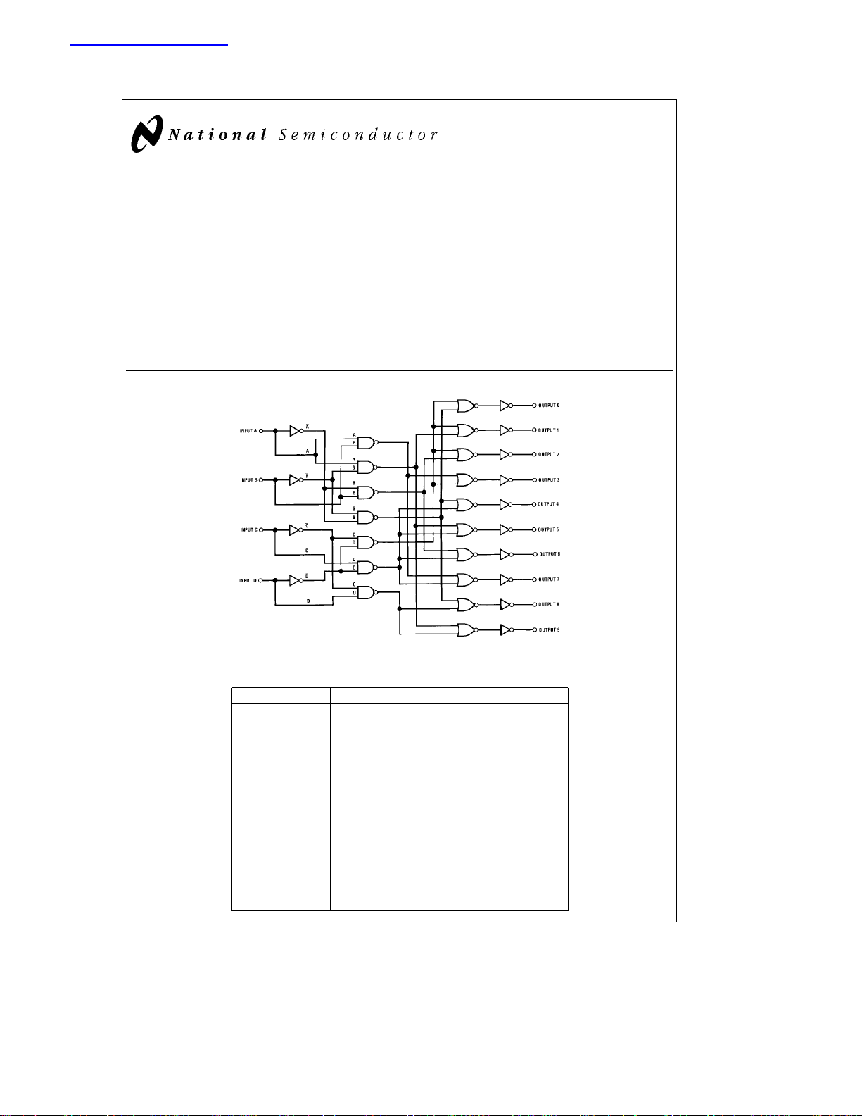
MM54C42/MM74C42 BCD-to-Decimal Decoder
MM54C42/MM74C42 BCD-to-Decimal Decoder
March 1988
General Description
The MM54C42/MM74C42 one-of-ten decoder is a monolithic complementary MOS (CMOS) integrated circuit constructed with N- and P-channel enhancement transistors.
This decoder produces a logical ‘‘0’’ at the output corresponding to a four bit binary input from zero to nine, and a
logical ‘‘1’’ at the other outputs. For binary inputs from ten to
fifteen all outputs are logical ‘‘1’’.
Features
Y
Supply voltage range 3V to 15V
Y
Tenth power TTL drive 2 LPTTL loads
compatible
Schematic Diagram
Y
High noise immunity 0.45 VCC(typ.)
Y
Low power 50 nW (typ.)
Y
Medium speed operation 10 MHz (typ.)
with 10V V
Applications
Y
Automotive
Y
Data terminals
Y
Instrumentation
Y
Medical electronics
Y
Alarm systems
Y
Industrial electronics
Y
Remote metering
Y
Computers
CC
TL/F/5882– 1
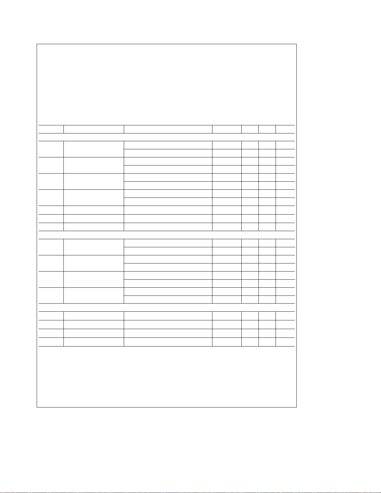
Truth Table
Inputs Outputs
DCBA0123456789
0 000 0111111111
0 001 1011111111
0 010 1101111111
0 011 1110111111
0 100 1111011111
0 101 1111101111
0 110 1111110111
0 111 1111111011
1 000 1111111101
1 001 1111111110
1 010 1111111111
1 011 1111111111
1 100 1111111111
1 101 1111111111
1 110 1111111111
1 111 1111111111
C
1995 National Semiconductor Corporation RRD-B30M105/Printed in U. S. A.
TL/F/5882
Absolute Maximum Ratings (Note 1)
b
If Military/Aerospace specified devices are required,
please contact the National Semiconductor Sales
Office/Distributors for availability and specifications.
Voltage at Any Pin (Note 1)
Operating Temperature Range
MM54C42
MM74C42
b
0.3V to V
b
b
a
0.3V
CC
55§Ctoa125§C
40§Ctoa85§C
Storage Temperature Range
Power Dissipation (PD)
Dual-In-Line 700 mW
Small Outline 500 mW
Operating V
Absolute Maximum V
Range 3.0V to 15V
CC
CC
Lead Temperature
65§Ctoa150§C
18V
(Soldering, 10 seconds) 260
DC Electrical Characteristics
Min/Max limits apply across temperature range unless otherwise noted
Symbol Parameter Conditions Min Typ Max Units
CMOS TO CMOS
V
IN(1)
V
IN(0)
V
OUT(1)
V
OUT(0)
I
IN(1)
I
IN(0)
I
CC
Logical ‘‘1’’ Input Voltage V
Logical ‘‘0’’ Input Voltage V
Logical ‘‘1’’ Output Voltage V
Logical ‘‘0’’ Output Voltage V
Logical ‘‘1’’ Input Current V
Logical ‘‘0’’ Input Current V
Supply Current V
CMOS/LPTTL INTERFACE
V
IN(1)
V
IN(0)
V
OUT(1)
V
OUT(0)
Logical ‘‘1’’ Input Voltage 54C, V
Logical ‘‘0’’ Input Voltage 54C, V
Logical ‘‘1’’ Output Voltage 54C, V
Logical ‘‘0’’ Output Voltage 54C, V
OUTPUT DRIVE (see 54C/74C Family Characteristics Data Sheet) T
I
SOURCE
I
SOURCE
I
SINK
I
SINK
Note 1: ‘‘Absolute Maximum Ratings’’ are those values beyond which the safety of the device cannot be guaranteed. Except for ‘‘Operating Temperature Range’’
they are not meant to imply that the devices should be operated at these limits. The table of ‘‘Electrical Characteristics’’ provides conditions for actual device
operation.
Output Source Current V
Output Source Current V
Output Sink Current V
Output Sink Current V
e
5.0V 3.5 V
CC
e
V
10V 8.0 V
CC
e
5.0V 1.5 V
CC
e
V
10V 2.0 V
CC
CC
V
CC
CC
V
CC
CC
CC
CC
74C, V
74C, V
74C, V
74C, V
CC
CC
CC
CC
e
e
e
e
e
e
e
e
e
e
e
eb
5.0V, I
10V, I
5.0V, I
10V, I
15V, V
15V, V
10 mA 4.5 V
O
eb
10 mA 9.0 V
O
e
10 mA 0.5 V
O
e
10 mA 1.0 V
O
e
15V 1.0 mA
IN
e
0V
IN
b
1.0 mA
15V 0.05 300 mA
e
4.5V V
CC
e
4.75V V
CC
e
4.5V 0.8 V
CC
e
4.75V 0.8 V
CC
e
CC
e
CC
e
CC
e
CC
5.0V, V
10V, V
5.0V, V
10V, V
4.5V, I
4.75V, I
4.5V, I
4.75V, I
IN(0)
IN(0)
IN(1)
IN(1)
eb
360 mA 2.4 V
O
eb
360 mA 2.4 V
O
e
360 mA 0.4 V
O
e
360 mA 0.4 V
O
e
25§C (short circuit current)
A
e
e
e
e
0V, V
0V, V
5.0V, V
10V, V
OUT
OUT
OUT
OUT
e
0V
e
0V
e
V
CC
e
V
CC
b
1.5 V
CC
b
1.5 V
CC
b
1.75 mA
b
8.0 mA
1.75 mA
8.0 mA
C
§
2
 Loading...