

查询MM54C192供应商
MM54C192/MM74C192
Synchronous 4-Bit Up/Down Decade Counter
MM54C193/MM74C193
Synchronous 4-Bit Up/Down Binary Counter
February 1988
MM54C192/MM74C192 Synchronous 4-Bit Up/Down Decade Counter
MM54C193/MM74C193 Synchronous 4-Bit Up/Down Binary Counter
General Description
These up/down counters are monolithic complementary
MOS (CMOS) integrated circuits. The MM54C192 and
MM74C192 are BCD counters, while the MM54C193 and
MM74C193 are binary counters.
Counting up and counting down is performed by two count
inputs, one being held high while the other is clocked. The
outputs change on the positive-going transition of this clock.
These counters feature preset inputs that are set when load
is a logical ‘‘0’’ and a clear which forces all outputs to ‘‘0’’
when it is at a logical ‘‘1’’. The counters also have carry and
borrow outputs so that they can be cascaded using no external circuitry.
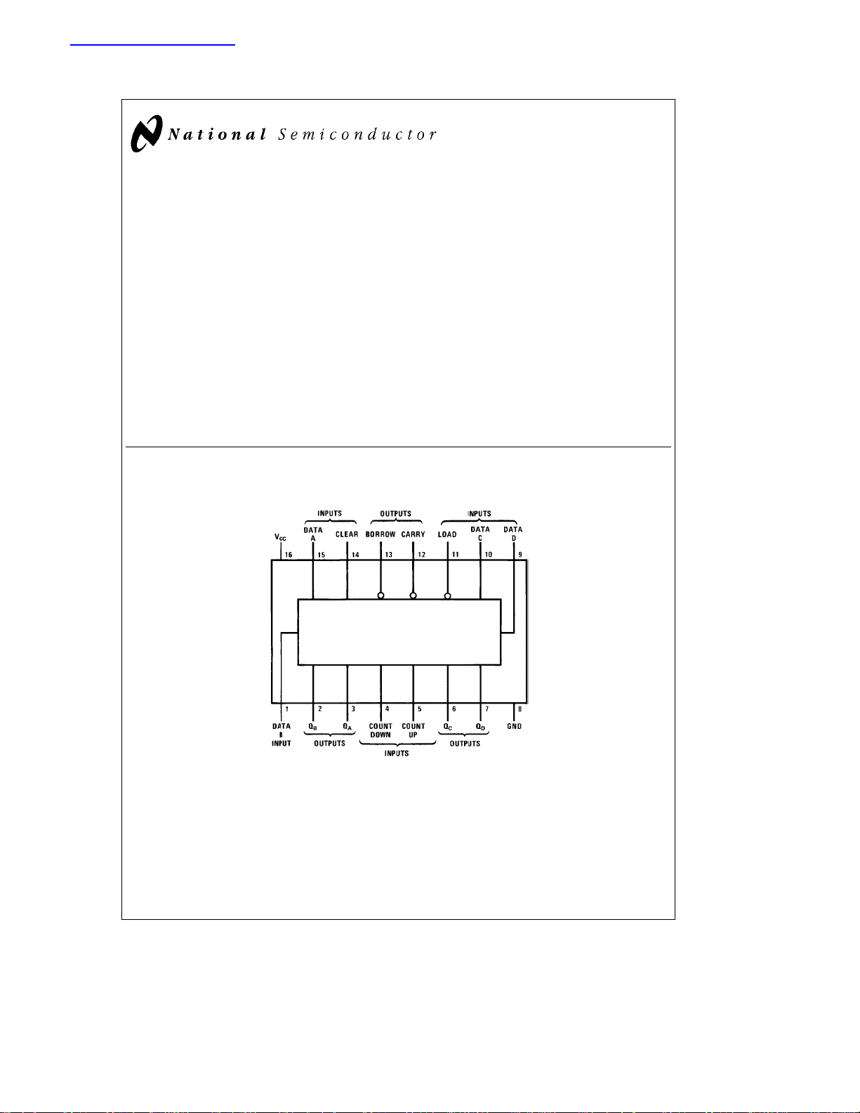
Connection Diagram
Dual-In-Line Package
Features
Y
High noise margin 1V guaranteed
Y
Tenth power TTL compatible Drive 2 LPTTL loads
Y
Wide supply range 3V to 15V
Y
Carry and borrow outputs for N-bit cascading
Y
Asynchronous clear
Y
High noise immunity 0.45 VCC(typ.)
Top View
Order Number MM54C192, MM74C192,
MM54C193 or MM74C193
C
1995 National Semiconductor Corporation RRD-B30M105/Printed in U. S. A.
TL/F/5901
TL/F/5901– 1
Absolute Maximum Ratings (Note 1)
If Military/Aerospace specified devices are required,
please contact the National Semiconductor Sales
Office/Distributors for availability and specifications.
Voltage at Any Pin
Operating Temperature Range (TA)
MM54C154
MM74C154
b
0.3V to V
b
b
a
0.3V
CC
55§Ctoa125§C
40§Ctoa85§C
Storage Temperature Range (T
)
S
Maximum VCCVoltage 18V
Power Dissipation (PD)
Dual-In-Line 700 mW
Small Outline 500 mW
Operating V
Range 3V to 15V
CC
Lead Temperature (TA)
65§Ctoa150§C
b
(Soldering, 10 sec.) 260
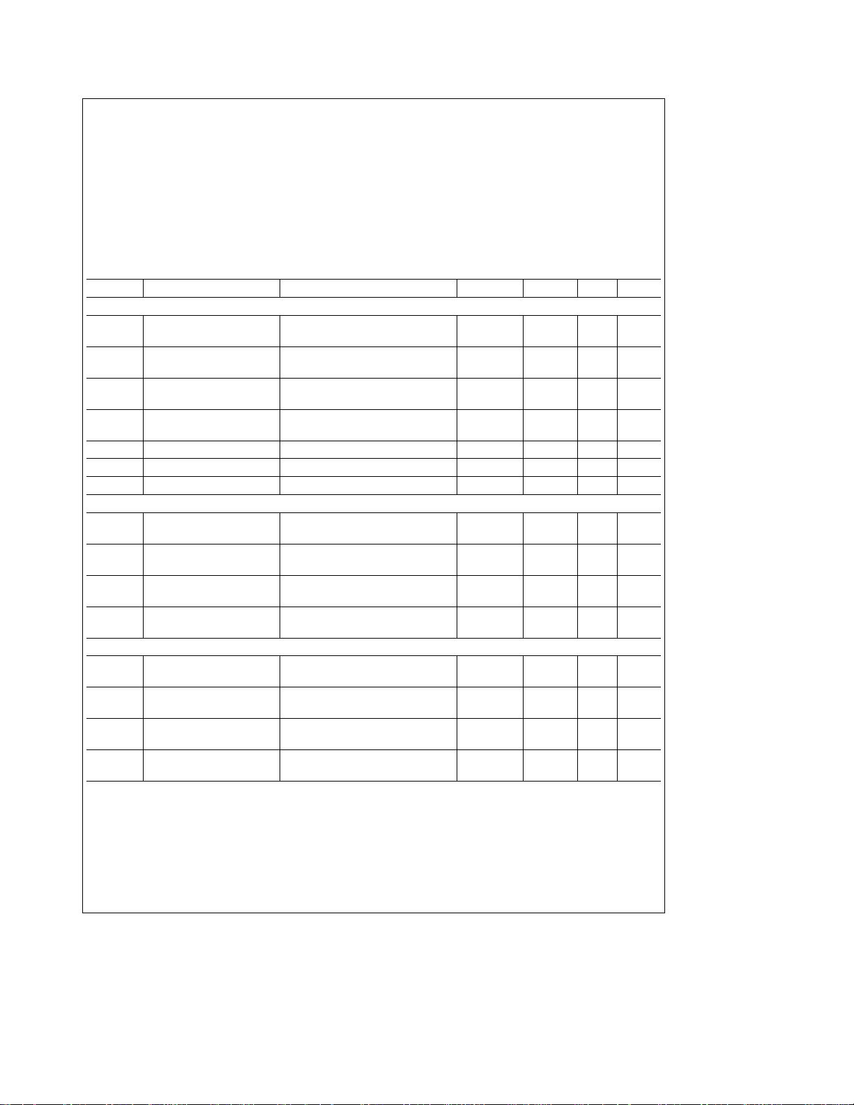
DC Electrical Characteristics Min/Max limits apply across temperature range unless otherwise noted
Symbol Parameter Conditions Min Typ Max Units
CMOS TO CMOS
V
IN(1)
V
IN(0)
V
OUT(1)
V
OUT(0)
I
IN(1)
I
IN(0)
I
CC
Logical ‘‘1’’ Input Voltage V
Logical ‘‘0’’ Input Voltage V
Logical ‘‘1’’ Output Voltage V
Logical ‘‘0’’ Output Voltage V
Logical ‘‘1’’ Input Current V
Logical ‘‘0’’ Input Current V
Supply Current V
CMOS TO LPTTL INTERFACE
V
IN(1)
V
IN(0)
V
OUT(1)
V
OUT(0)
Logical ‘‘1’’ Input Voltage 54C V
Logical ‘‘0’’ Input Voltage 54C V
Logical ‘‘1’’ Output Voltage 54C V
Logical ‘‘0’’ Output Voltage 54C V
OUTPUT DRIVE (See 54C/74C Family Characteristics Data Sheet) (Short Circuit Current)
I
SOURCE
I
SOURCE
I
SINK
I
SINK
Note 1: ‘‘Absolute Maximum Ratings’’ are those values beyond which the safety of the device cannot be guaranteed. Except for ‘‘Operating Temperature Range’’
they are not meant to imply that the devices should be operated at these limits. The table of ‘‘Electrical Characteristics’’ provides conditions for actual device
operation.
Output Source Current V
Output Source Current V
Output Sink Current V
Output Sink Current V
e
5V 3.5 V
CC
e
V
10V 8.0 V
CC
e
5V 1.5 V
CC
e
V
10V 2.0 V
CC
e
eb
5V, I
CC
e
V
10V, I
CC
e
5V, I
CC
e
V
10V, I
CC
e
15V, V
CC
e
15V, V
CC
e
15V 0.05 300 mA
CC
CC
74C V
CC
CC
74C V
CC
CC
74C V
CC
CC
74C V
CC
e
5V, V
CC
e
25§C, V
T
A
e
10V, V
CC
e
25§C, V
T
A
e
5V, V
CC
e
T
25§C, V
A
e
10V, V
CC
e
T
25§C, V
A
10 mA 4.5 V
O
eb
10 mA 9.0 V
O
e
10 mA 0.5 V
O
e
10 mA 1.0 V
O
e
15V 0.005 1.0 mA
IN
e
0V
IN
e
4.5V V
e
4.75V V
e
4.5V 0.8 V
e
4.75V 0.8 V
e
e
e
e
4.5V, I
4.75V, I
4.5V, I
4.75V, I
IN(0)
OUT
IN(0)
OUT
IN(1)
OUT
IN(1)
OUT
eb
100 mA 2.4 V
O
eb
100 mA 2.4 V
O
e
360 mA 0.4 V
O
e
360 mA 0.4 V
O
e
0V
e
0V
e
0V
e
0V
e
5V
e
V
CC
e
10V
e
V
CC
b
1.0
b
CC
b
CC
b
1.75 mA
b
b
0.005 mA
1.5 V
1.5 V
8mA
1.75 mA
8mA
C
§
2

AC Electrical Characteristics* T
e
A
25§C, C
e
50 pF, unless otherwise noted
L
Symbol Parameter Conditions Min Typ Max Units
t
pd
t
pd
t
pd
t
S
t
W
t
W
t
pd0,tpd1
t
W
f
MAX
tr,t
f
C
IN
C
PD
*AC Parameters are guaranteed by DC correlated testing.
Note 1: ‘‘Absolute Maximum Ratings’’ are those values beyond which the safety of the device cannot be guaranteed. Except for ‘‘Operating Temperature Range’’
they are not meant to imply that the devices should be operated at these limits. The table of ‘‘Electrical Characteristics’’ provides conditions for actual device
operation.
Note 2: Capacitance is guaranteed by periodic testing.
Note 3: C
PD
AN-90.
Propagation Delay Time to Q V
from Count Up or Down V
Propagation Delay Time to Q V
Borrow from Count Down V
Propagation Delay Time to V
Carry from Count Up V
Time Prior to Load that Data V
Must be Present V
Minimum Clear Pulse Width V
Minimum Load Pulse Width V
Propagation Delay Time to Q V
from Load V
Minimum Count Pulse Width V
Maximum Count Frequency V
Count Rise and Fall Time V
Input Capacitance (Note 2) 5 pF
Power Dissipation Capacitance (Note 3) 100 pF
determines the no load AC power consumption of any CMOS device. For complete explanation, see 54C/74C Family Characteristics, Application Note
e
5V 250 400 ns
CC
e
10V 100 160 ns
CC
e
5V 120 200 ns
CC
e
10V 50 80 ns
CC
e
5V 120 200 ns
CC
e
10V 50 80 ns
CC
e
5V 100 160 ns
CC
e
10V 30 50 ns
CC
e
5V 300 480 ns
CC
e
V
10V 120 190 ns
CC
e
5V 100 160 ns
CC
e
V
10V 40 65 ns
CC
e
5V 300 480 ns
CC
e
10V 120 190 ns
CC
e
5V 120 200 ns
CC
e
V
10V 35 80 ns
CC
e
5V 2.5 4 MHz
CC
e
V
10V 6 10 MHz
CC
e
5V 15 ms
CC
e
V
10V 5 ms
CC
Cascading Packages
Guaranteed Noise Margin
as a Function of V
TL/F/5901– 2
CC
TL/F/5901– 3
3

Timing Diagrams
MM54C192/MM74C192
Note 1: Clear ouptuts to zero.
Note 2: Load (preset) to binary thirteen.
Note 3: Count up to fourteen, fifteen, carry, zero, one and two.
Note 4: Count down to one, zero, borrow, fifteen, fourteen, and thirteen.
MM54C193/MM74C193
Note 1: Clear ouptuts to zero.
Note 2: Load (preset) to BCD seven.
Note 3: Count up to eight, nine, carry, zero, one, and two.
Note 4: Count down to one, zero, borrow, nine, eight, and seven.
Note A: Clear overrides load, data, and count inputs.
Note B: When counting up, count down input must be high; when counting down, count-up input must be high.
TL/F/5901– 4
TL/F/5901– 5
4

Schematic Diagrams
MM54C192 Synchronous 4-Bit Up/Down Decade Counter
MM54C193 Synchronous 4-Bit Up/Down Binary Counter
TL/F/5901– 6
TL/F/5901– 7
5

Physical Dimensions inches (millimeters)
Order Number MM54C192J, MM74C192J, MM54C193J or MM74C193J
Ceramic Dual-In-Line Package (J)
NS Package Number J16A
Molded Dual-In-Line Package (N)
Order Number MM54C192N, MM74C192N, MM54C193N or MM74C193N
NS Package Number N16E
MM54C193/MM74C193 Synchronous 4-Bit Up/Down Binary Counter
LIFE SUPPORT POLICY
MM54C192/MM74C192 Synchronous 4-Bit Up/Down Decade Counter
NATIONAL’S PRODUCTS ARE NOT AUTHORIZED FOR USE AS CRITICAL COMPONENTS IN LIFE SUPPORT
DEVICES OR SYSTEMS WITHOUT THE EXPRESS WRITTEN APPROVAL OF THE PRESIDENT OF NATIONAL
SEMICONDUCTOR CORPORATION. As used herein:
1. Life support devices or systems are devices or 2. A critical component is any component of a life
systems which, (a) are intended for surgical implant support device or system whose failure to perform can
into the body, or (b) support or sustain life, and whose be reasonably expected to cause the failure of the life
failure to perform, when properly used in accordance support device or system, or to affect its safety or
with instructions for use provided in the labeling, can effectiveness.
be reasonably expected to result in a significant injury
to the user.
National Semiconductor National Semiconductor National Semiconductor National Semiconductor
Corporation Europe Hong Kong Ltd. Japan Ltd.
1111 West Bardin Road Fax: (
Arlington, TX 76017 Email: cnjwge@tevm2.nsc.com Ocean Centre, 5 Canton Rd. Fax: 81-043-299-2408
Tel: 1(800) 272-9959 Deutsch Tel: (
Fax: 1(800) 737-7018 English Tel: (
National does not assume any responsibility for use of any circuitry described, no circuit patent licenses are implied and National reserves the right at any time without notice to change said circuitry and specifications.
Fran3ais Tel: (
Italiano Tel: (
a
49) 0-180-530 85 86 13th Floor, Straight Block, Tel: 81-043-299-2309
a
49) 0-180-530 85 85 Tsimshatsui, Kowloon
a
49) 0-180-532 78 32 Hong Kong
a
49) 0-180-532 93 58 Tel: (852) 2737-1600
a
49) 0-180-534 16 80 Fax: (852) 2736-9960
 Loading...