

查询LM121AH/883供应商
LM221/LM321 Precision Preamplifiers
General Description
The LM221 series are precision preamplifiers designed to
operate with general purpose operational amplifiers to drastically decrease dc errors. Drift, bias current, common mode
and supply rejection are more than a factor of 50 better than
standard op amps alone. Further, the added dc gain of the
LM221 decreases the closed loop gain error.
The LM221 series operates with supply voltages from
g
to
20V and has sufficient supply rejection to operate from
unregulated supplies. The operating current is programmable from 5 m Ato200mA so bias current, offset current, gain
and noise can be optimized for the particular application
while still realizing very low drift. Super-gain transistors are
used for the input stage so input error currents are lower
than conventional amplifiers at the same operating current.
Further, the initial offset voltage is easily nulled to zero.
The extremely low drift of the LM221 will improve accuracy
on almost any precision dc circuit. For example, instrumentation amplifier, strain gauge amplifiers and thermocouple
amplifiers now using chopper amplifiers can be made with
the LM221. The full differential input and high commonmode rejection are another advantage over choppers. For
applications where low bias current is more important than
drift, the operating current can be reduced to low values.
High operating currents can be used for low voltage noise
with low source resistance. The programmable operating
current of the LM221 allows tailoring the input characteris-
g
3V
tics to match those of specialized op amps.
The LM221 is specified over a
the LM321 over a 0
Ctoa70§C temperature range.
§
b
25§Ctoa85§C range and
Features
Y
Guaranteed drift of LM321AÐ0.2 mV/§C
Y
Guaranteed drift of LM221 seriesÐ1 mV/§C
Y
Offset voltage less than 0.4 mV
Y
Bias current less than 10 nA at 10 mA operating current
Y
CMRR 126 dB minimum
Y
120 dB supply rejection
Y
Easily nulled offset voltage
LM221/LM321 Precision Preamplifiers
February 1995
Typical Applications
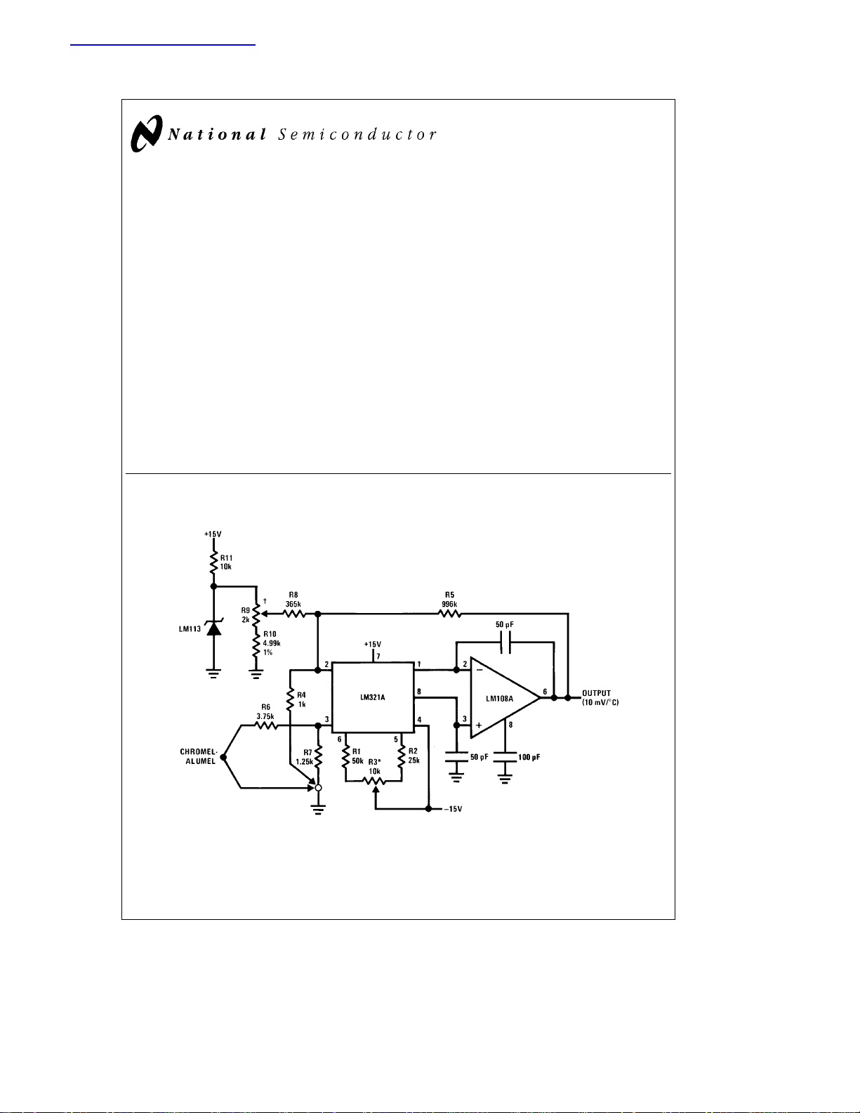
Thermocouple Amplifier with Cold Junction Compensation
*Set for 2.98V at output with LM113
shorted. Output should equal ambient temperature at 10 mV/
²
Adjust for output reading in§C.
K.
§
TL/H/7769– 1
C
1995 National Semiconductor Corporation RRD-B30M115/Printed in U. S. A.
TL/H/7769
Absolute Maximum Ratings
Supply Voltage
Power Dissipation (Note 1) 500 mW
Differential Input Voltage (Notes 2 and 3)
Input Voltage (Note 3)
g
20V
g
15V
g
15V
Operating Temperature Range
LM321A 0
Storage Temperature Range
Ctoa70§C
§
b
65§Ctoa150§C
Lead Temperature (Soldering, 10 sec.) 300
ESD rating to be determined.
Electrical Characteristics (Note 4) LM321A
Parameter Conditions
Input Offset Voltage T
Input Offset Current T
Input Bias Current T
Input Resistance T
Supply Current T
e
25§C, 6.4ksR
A
e
25§C,
A
R
SET
R
SET
e
25§C,
A
R
SET
R
SET
e
25§C,
A
R
SET
R
SET
e
25§C, R
A
Input Offset Voltage 6.4ksR
Input Bias Current R
Input Offset Current R
Input Offset Current Drift R
Average Temperature R
e
SET
e
R
SET
e
SET
e
R
SET
e
SET
s
200X, 6.4ksR
S
s
70k 0.2 0.4 mV
SET
e
70k 0.3 0.5 nA
e
6.4k 5 nA
e
70k 5 15 nA
e
6.4k 50 150 nA
e
70k 2 8 MX
e
6.4k 0.2 MX
e
70k 0.8 2.2 mA
SET
s
70k 0.5 0.65 mV
SET
70k 15 25 nA
6.4k 150 250 nA
70k 0.5 1 nA
6.4k 5 10 nA
70k 3 pA/§C
s
70k
SET
Min Typ Max
Coefficient of Input Offset Offset Voltage Nulled
Voltage 0.07 0.2 mV/
Long Term Stability 3 mV/yr
Supply Current 1 3.5 mA
e
Input Voltage Range V
Common-Mode Rejection R
Ratio R
Supply Voltage Rejection R
Ratio R
Voltage Gain T
Noise R
Note 1: The maximum junction temperature of the LM321A is 85§C. For operating at elevated temperature, devices in the H08 package must be derated based on
a thermal resistance of 150
Note 2: The inputs are shunted with back-to-back diodes in series with a 500X resistor for overvoltage protection. Therefore, excessive current will flow if a
differential input voltage in excess of 1V is applied between the inputs.
Note 3: For supply voltages less than
Note 4: These specifications apply for
specifications are limited to
Note 5: External precision resistor Ð0.1%Ð can be placed from pins 1 and 8 to 7 increase positive common-mode range.
Note 6: See RETS121X for LM121H/883 military specs and RET121AX for LM121AH/883 military specs.
C/W, junction to ambient, or 18§C/W, junction to case.
§
g
g
b
25§CsT
g
15V, (Note 5)
S
e
R
70k
SET
e
R
6.4k
SET
e
70k 126 140 dB
SET
e
6.4k 120 130 dB
SET
e
70k 118 126 dB
SET
e
6.4k 114 120 dB
SET
e
25§C, R
A
l
R
3MX 12 20 V/V
L
e
SET
15V, the absolute maximum input voltage is equal to the supply voltage.
s
g
5sV
A
s
20V andb55§CsT
S
a
85§C, and for the LM321A the specifications apply over a 0§Ctoa70§C temperature range.
70k, R
SET
SOURCE
e
70k,
e
0 8 nV/0Hz
s
a
125§C, unless otherwise specified. With the LM221A, however all temperature
A
g
a7,b
LM321A
Units
13 V
13 V
C
§
C
§
2
Absolute Maximum Ratings
If Military/Aerospace specified devices are required,
please contact the National Semiconductor Sales
Office/Distributors for availability and specifications.
Supply Voltage
g
20V
Power Dissipation (Note 1) 500 mW
g
Differential Input Voltage (Notes 2 and 3)
Input Voltage (Note 3)
15V
g
15V
Operating Temperature Range
LM221, LM121A (-883), LM121 (-883)
LM321, LM321A 0
Storage Temperature Range
b
25§Ctoa85§C
Ctoa70§C
§
b
65§Ctoa150§C
Lead Temperature (Soldering, 10 sec.) 260§C
ESD rating to be determined.
Electrical Characteristics (Note 4) LM221, LM321
Parameter Conditions
Input Offset Voltage T
Input Offset Current T
Input Bias Current T
Input Resistance T
Supply Current T
Input Offset Voltage 6.4ksR
Input Bias Current R
Input Offset Current R
Input Offset Current Drift R
Average Temperature R
Coefficient of Input Offset Voltage Nulled 1 1 mV/
e
25§C, 6.4ksR
A
e
25§C,
A
e
R
70k 1 2 nA
SET
e
R
6.4k 10 20 nA
SET
e
25§C,
A
e
R
70k 10 18 nA
SET
e
R
6.4k 100 180 nA
SET
e
25§C,
A
e
R
70k 4 2 MX
SET
e
R
6.4k 0.4 0.2 MX
SET
e
25§C, R
A
SET
R
SET
SET
R
SET
SET
s
S
SET
s
70k 1.0 2.5 mV
SET
e
70k 30 28 nA
e
6.4k 300 280 nA
e
70k 3 4 nA
e
6.4k 30 40 nA
e
70k 3 3 pA/§C
200X, 6.4ksR
s
70k 0.7 1.5 mV
SET
e
70k 1.5 2.2 mA
s
70k
SET
Offset Voltage
Long Term Stability 5 5 mV/yr
Supply Current 2.5 3.5 mA
e
Input Voltage Range V
Common-Mode Rejection R
Ratio R
Supply Voltage Rejection R
Ratio R
Voltage Gain T
Noise R
Note 1: The maximum junction temperature of the LM221 is 100§C. The maximum junction temperature of the LM321 is 85§C. For operating at elevated
temperature, devices in the H08 package must be derated based on a thermal resistance of 150
Note 2: The inputs are shunted with back-to-back diodes in series with a 500X resistor for overvoltage protection. Therefore, excessive current will flow if a
differential input voltage in excess of 1V is applied between the inputs.
Note 3: For supply voltages less than
Note 4: These specifications apply for
specifications are limited to
Note 5: External precision resistor Ð0.1%Ð can be placed from pins 1 and 8 to 7 increase positive common-mode range.
b
25§CsT
g
15V, (Note 5)
S
e
R
70k
SET
e
R
6.4k
SET
e
70k 120 114 dB
SET
e
6.4k 114 114 dB
SET
e
70k 120 114 dB
SET
e
6.4k 114 114 dB
SET
e
25§C, R
A
l
R
3MX 16 12 V/V
L
e
SET
g
15V, the absolute maximum input voltage is equal to the supply voltage.
g
5sV
s
a
A
e
70k,
SET
70k, R
s
g
S
85§C, and for the LM321 the specifications apply over a 0§Ctoa70§C temperature range.
e
SOURCE
20V andb55§CsT
0 8 8 nV/0Hz
s
A
LM221 LM321
Min Typ Max Min Typ Max
g
13
a7,b
13
C/W, junction to ambient, or 18§C/W, junction to case.
§
a
125§C, unless otherwise specified. With the LM221, however all temperature
g
13 V
a7,b
13 V
Units
C
§
3
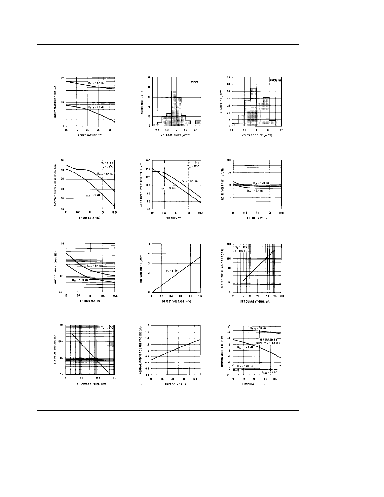
Typical Performance Characteristics
Input Bias Current Voltage Drift (Nulled)
Positive Power Supply
Rejection
Input Noise Current Voltage Drift Differential Voltage Gain
Distribution of Offset
Negative Power Supply
Rejection
Distribution of Offset
Voltage Drift (Nulled)
Input Noise Voltage
Set Resistor and Set Current Set Current Common-Mode Limits
TL/H/7769– 9
4

Typical Performance Characteristics (Continued)
Common-Mode Limits Output Common-Mode Voltage Differential Voltage Gain
Supply Current Offset Voltage Adjustment Ratio
Connection Diagram
Order Number LM121AH/883, LM121H/883,
LM221H, LM321H or LM321AH
See NS Package Number H08C
Note: Outputs are inverting from the input of the same number.
Common-Mode Rejection
TL/H/7769– 10
Metal Can Package
TL/H/7769– 7
Top View
Note: Pin 4 connected to case.
5

Schematic Diagram
TL/H/7769– 8
6

Frequency Compensation
UNIVERSAL COMPENSATION
The additional gain of the LM321 preamplifier when used
with an operational amplifier usually necessitates additional
frequency compensation. When the closed loop gain of the
op amp with the LM321 is less than the gain of the LM321
alone, more compensation is needed. The worst case situation is when there is 100% feedbackÐsuch as a voltage
follower or integratorÐand the gain of the LM321 is high.
When high closed loop gains are usedÐfor example A
1000Ðand only an addition gain of 200 is inserted by the
LM321, the frequency compensation of the op amp will usually suffice.
The frequency compensation shown here is designed to operate with any unity-gain stable op amp.
Figure 1
basic configuration of frequency stabilizing network. In operation the output of the LM321 is rendered single ended by a
0.01 mF bypass capacitor to ground. Overall frequency compensation then is achieved by an integrating capacitor
around the op amp.
12
Bandwidth at unity-gain
for 0.5 MHz bandwidth C
j
2qR
C
SET
4
e
106R
SET
For use with higher frequency op amps such as the LM118
the bandwidth may be increased to about 2 MHz.
If the closed loop gain is greater than unity, ‘‘C’’ may be
decreased to:
4
e
C
106ACLR
SET
ALTERNATE COMPENSATION
The two compensation capacitors can be made equal for
improved power supply rejection. In this case the formula for
the compensation capscitor is:
8
e
C
106ACLR
SET
V
shows the
Table I shows typical values for the two compensating capacitors for various gains and operating currents.
TABLE I
Closed
Loop
Gain
e
A
V
A
V
A
V
A
V
e
A
V
e
A
V
e
A
V
120 kX 60 kX 30 kX 12 kX 6kX
e
1 68 130 270 680 1300
e
5 15 27 56 130 270
e
10 10 15 27 68 130
e
50 1 3 5 15 27
100 – 1 3 5 10
500 – – 1 1 3
1000 – – – – –
Current Set Resistor
This table applies for the LM108, LM101A, LM741, LM118.
Capacitance is in pF.
DESIGN EQUATIONS FOR THE LM321 SERIES
6
c
10
1.2
&
Gain A
V
R
Null Pot Value should be 10% of R
Operating Current
Positive Common-Mode Limit&V
SET
SET
c
2
0.65V
&
R
SET
0.6
Ð
0.65Vc50k
b
R
SET
(
a
b
Typical Applications
*Offset adjust.
²
See table for frequency compensation.
FIGURE 1. Low Drift Op Amp Using the LM321A as a Preamp
TL/H/7769– 2
7

Typical Applications (Continued)
Gain of 1000 Instrumentation Amplifier
High Speed* Inverting Amplifier with Low Drift
³
*Offset adjust
²
Gain trim
³
Better than 1% linearity for input sig-
g
nals up to
cal
Match of R5 and R6 effect power
supply rejection
10 mV gain stability typi-
a
2% fromb55 toa125§C.
TL/H/7769– 3
Medium Speed* General Purpose Amplifier
8
*Bandwidthe10 MHz
*Bandwidthe3.5 MHz
Slew Rate
Slew Rate
TL/H/7769– 5
e
40 V/ms
TL/H/7769– 4
e
1.1 V/ms

Typical Applications (Continued)
Increased Common-Mode Range at High Operating Currents
*Match to 0.1%
²
Depends on close loop gain
TL/H/7769– 6
9

Physical Dimensions inches (millimeters)
LM221/LM321 Precision Preamplifiers
Order Number LM221H, LM321H or LM321AH
Metal Can Package (H)
NS Package Number H08C
LIFE SUPPORT POLICY
NATIONAL’S PRODUCTS ARE NOT AUTHORIZED FOR USE AS CRITICAL COMPONENTS IN LIFE SUPPORT
DEVICES OR SYSTEMS WITHOUT THE EXPRESS WRITTEN APPROVAL OF THE PRESIDENT OF NATIONAL
SEMICONDUCTOR CORPORATION. As used herein:
1. Life support devices or systems are devices or 2. A critical component is any component of a life
systems which, (a) are intended for surgical implant support device or system whose failure to perform can
into the body, or (b) support or sustain life, and whose be reasonably expected to cause the failure of the life
failure to perform, when properly used in accordance support device or system, or to affect its safety or
with instructions for use provided in the labeling, can effectiveness.
be reasonably expected to result in a significant injury
to the user.
National Semiconductor National Semiconductor National Semiconductor National Semiconductor
Corporation Europe Hong Kong Ltd. Japan Ltd.
1111 West Bardin Road Fax: (
Arlington, TX 76017 Email: cnjwge@tevm2.nsc.com Ocean Centre, 5 Canton Rd. Fax: 81-043-299-2408
Tel: 1(800) 272-9959 Deutsch Tel: (
Fax: 1(800) 737-7018 English Tel: (
National does not assume any responsibility for use of any circuitry described, no circuit patent licenses are implied and National reserves the right at any time without notice to change said circuitry and specifications.
Fran3ais Tel: (
Italiano Tel: (
a
49) 0-180-530 85 86 13th Floor, Straight Block, Tel: 81-043-299-2309
a
49) 0-180-530 85 85 Tsimshatsui, Kowloon
a
49) 0-180-532 78 32 Hong Kong
a
49) 0-180-532 93 58 Tel: (852) 2737-1600
a
49) 0-180-534 16 80 Fax: (852) 2736-9960

This datasheet has been download from:
www.datasheetcatalog.com
Datasheets for electronics components.
 Loading...