

National Semiconductor LM2202 Technical data

查询LM2202供应商
LM2202
230 MHz Video Amplifier System
General Description
The LM2202 is a very high frequency video amplifier system
intended for use in high resolution monochrome or RGB
color monitor applications. In addition to the wideband video
amplifier theLM2202contains a gated differential input black
level clamp comparator for brightness control, a DC controlled attenuator for contrast control and a DC controlled
sub contrast attenuator for drive control. The DC control for
the contrast attenuator is pinned out separately to provide a
more accurate control system for RGB color monitor applications. All DC controls offer a high input impedance and operate over a 0V to 4V range for easy interface to bus controlled
alignment systems. The LM2202 operates from a nominal
12V supply but can be operated with supply voltages down
to 8V for applications that require reduced IC package power
dissipation characteristics.
Features
n Wideband video amplifier
(f
−3dB
=
230 MHz at V
LM2202 230 MHz Video Amplifier System
April 1999
=
n t
1.5 ns at V
r,tf
n Externally gated comparator for brightness control
n 0V to 4V high input impedance DC contrast control
>
(
40 dB range)
n 0V to 4V high input impedance DC drive control
±
(
3 dB range)
n Easy to parallel three LM2202s for optimum color
tracking in RGB systems
n Output stage clamps to 0.65V and provides up to 9V
output voltage swing
n Output stage directly drives most hybrid or discrete CRT
amplifier stages
n Replacement for the LM1202
Applications
n High resolution CRT monitors
n Video switches
n Video AGC amplifier
=
)
4V
O
PP
n Wideband amplifier with gain and DC offset control
=
4V
O
PP
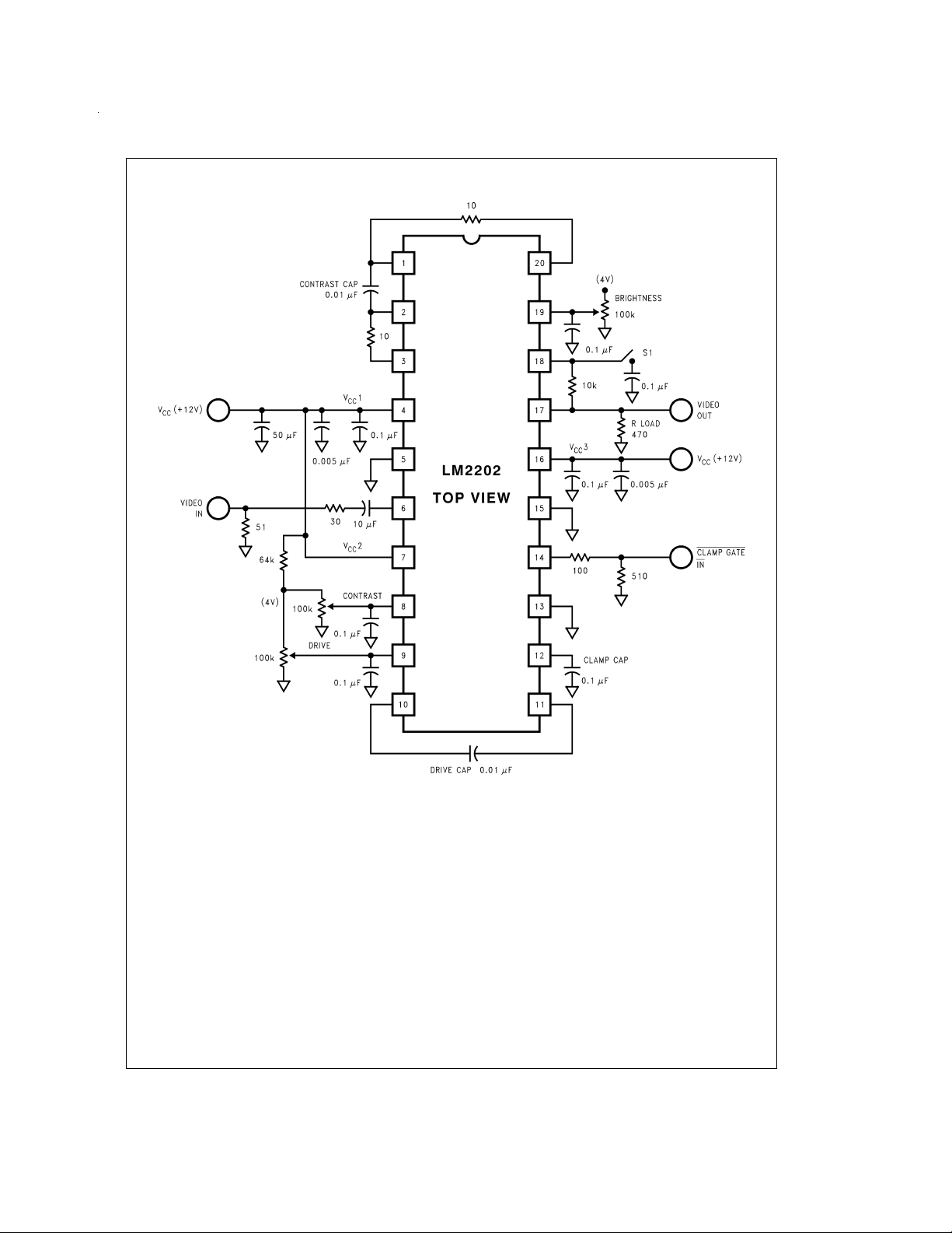
Block and Connection Diagram
Order Number LM2202N or LM2202M
See NS Package Number N20A or M20B
DS012591-1
© 1999 National Semiconductor Corporation DS012591 www.national.com
Absolute Maximum Ratings (Note 1)
If Military/Aerospace specified devices are required,
please contact the National Semiconductor Sales Office/
Distributors for availability and specifications.
Supply Voltage V
Ground Pins 5, 13, 15 13.5V
Voltage at Any Input Pin (V
Video Output Current (I
Package Power Dissipation at
=
25˚C 1.56W
T
A
(Above 25˚C Derate Based θ
Pins 4, 7, 16 to
CC
)V
IN
)28mA
17
and TJ)
JA
≥ VIN≥ GND
CC
Package Thermal Resistance (θ
N20A 68˚C/W
M20B 90˚C/W
Junction Temperature (T
Storage Temperature Range (T
Lead Temperature
N Package (Soldering, 10 sec.) 265˚C
ESD Susceptibility
Human Body Model: 100 pF
Discharged through a 1.5k
Resistor 1.5 kV
Operating Ratings (Note 2)
Temperature Range −20˚C to +80˚C
Supply Voltage (V
DC Electrical Characteristics
See Test Circuit (
wise noted.
Figure 1
Symbol Parameter Conditions
4, 7, 16 Total Supply Current R
I
S
V
6
V
14L
V
14H
I
14L
I
14H
I
12+
I
12−
V
17L
V
17H
V
OS
Video Input Bias Voltage 2.4 2 V (min)
Clamp Gate Low Input Voltage Clamp Comparator On 0.8 V (max)
Clamp Gate High Input Voltage Clamp Comparator Off 2 V (min)
Clamp Gate Low Input Current V
Clamp Gate High Input Current V
Clamp Cap Charge Current V
Clamp Cap Discharge Current V
Video Output Low Voltage V
Video Output High Voltage V
Comparator Input Offset Voltage V18−V
=
), T
25˚C, V4=V7=V16=12V, S1 Open, V19=4V, V8=4V, V9=4V, V14=0V unless other-
A
=
∞
LOAD
14
14
12
12
12
12
(Note 5) 48 60 mA (max)
=
0V −0.5 µA
=
12V 0.005 µA
=
0V 800 500 µA (min)
=
5V −800 −500 µA (min)
=
0V 0.2 0.65 V (max)
=
6V 10 9 V (min)
19
)
JA
) 150˚C
J
) −65˚C to +150˚C
stg
)8V≤V
CC
Typical
(Note 3)
15
Limit (Note
4)
±
50 mV (max)
CC
≤ 13.2V
Units
AC Electrical Characteristics
See Test Circuit (
erwise noted.
Figure 1
Symbol Parameter Conditions
R
IN
A
max Video Amplifier Gain V
V
∆A
V
∆A
V
Video Amplifier Input Resistance f
2V Attenuation at 2V Ref: AVmax, V
0.5V Attentuation at 0.5V Ref: AVmax, V
∆ Drive ∆ Gain Range V
THD Video Amplifier Distortion V
f
−3 dB
t
r
t
f
Note 1: Absolute Maximum Ratings indicate limits beyond which damage to the device may occur.
Note 2: Operating Ratings indicate conditions for which the device is functional but do not guarantee specific performance limits. For guaranteed specifications and
test conditions see the Electrical Characteristics. The guaranteed specifications apply only for the test conditions listed. Some performance characteristics may degrade when the device is not operated under the listed test conditions.
Note 3: Typical specifications are specified at +25˚C and represent the most likely parametric norm.
Note 4: Tested limits are guaranteed to National’s AOQL (Average Outgoing Quality Level).
Note 5: The supply current specified is the quiescent current for V
pends on the output load, R
bient temperature.
Note 6: When measuring video amplifier bandwidth or pulse rise and fall times, a double sided full ground plane printed circuit board is recommended. The measured
rise and fall times are effective rise and fall times, taking into account the rise and fall times of the generator and the oscilloscope.
www.national.com 2
Video Amplifier Bandwidth (Note 6) V
Output Rise Time (Note 6) V
Output Fall Time (Note 6) V
=
), T
25˚C, V4=V7=V16=12V, S1 Closed, V19=4V, V8=4V, V9=4V, V14=0V unless oth-
A
. The increase in device power dissipation due to R
Load
CC1,VCC2
Typical
(Note 3)
=
12 kHz 20 kΩ
IN
=
8
=
9
O
O
O
O
=
4V, V
4V 20 16 V/V (min)
9
=
2V −6 dB
8
=
0.5V −38 −23 dB (min)
8
0V to 4V 6 5 dB (min)
=
=
=
=
and V
4V
4V
4V
4V
=
12 kHz 0.5 1
PP,fIN
PP
PP
PP
=
Load
∞
, see
with R
CC3
must be taken into account when operating the device at the maximum am-
Load
230 MHz
1.5 2 ns (max)
1.5 2 ns (max)
Figure 1’s
test circuit. The total supply current also de-
Limit (Note
4)
Units
%
(max)
Test Circuit
FIGURE 1. LM2202 Test Circuit
DS012591-2
www.national.com3
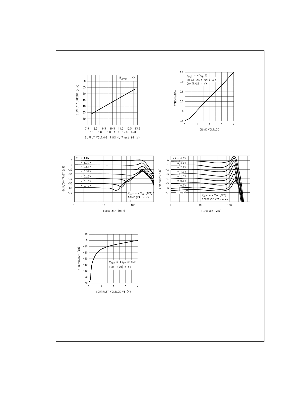
Typical Performance Characteristics (V
Quiescent Supply Current
vs Supply Voltage
DS012591-3
=
CC
12V, T
=
25˚C unless otherwise specified)
A
Attenuation vs Drive Voltage
DS012591-4
Contrast vs Frequency
Attenuation vs
Contrast Voltage
DS012591-7
DS012591-5
Drive vs Frequency
DS012591-6
Circuit Description
Figure 2
shows a block diagram of the LM2202 video amplifier along with contrast and brightness (black level) control.
Contrast control is a DC-operated attenuator which varies
the AC gain of the amplifier. Signal attenuation (contrast) is
achieved by varying the base drive to a differential pair and
thereby unbalancing the current through the differential pair.
As shown in
www.national.com 4
Figure 2
, pin 20 provides a 5.3V bias voltage for
the positive input of the attenuator (pin 1). Pin 3 provides a
control voltage for the negative input (pin 2) of the attenuator.
The voltage at pin 3 varies as the voltage at the contrast control input (pin 8) varies thus providing signal attenuation. The
gain is maximum (0 dB attenuation) if the voltage at pin 8 is
4V and is minimum (maximum attenuation) if the voltage at
pin 8 is 0V. The 0V to 4V DC-operated drive control at pin 9
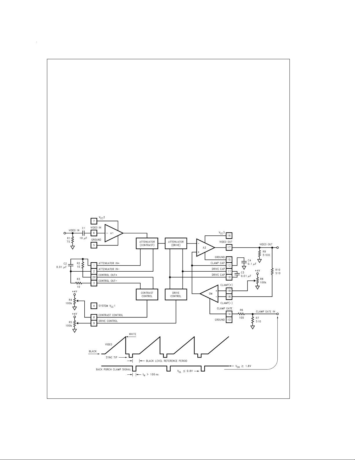
Circuit Description (Continued)
providesa6dBgain adjustment range. This feature is necessary for RGB applications where independent gain adjustment of each channel is required.
The brightness or black level clamping requires a “sample
and hold” circuit which holds the DC bias of the video amplifier constant during the black level reference portion of the
video waveform. Black level clamping, often referred to as
DC restoration, is accomplished by applying a back porch
clamp signal to the clamp gate input pin (pin 14). The clamp
comparator is enabled when the clamp signal goes low during the black level reference period (see
clamp comparator is enabled, the clamp capacitor connected to pin 12 is either charged or discharged until the voltage at the minus input of the comparator matches the voltage set at the plus input of the comparator. During the video
portion of the signal, the clamp comparator is disabled and
the clamp capacitor holds the proper DC bias. In a DC
coupled cathode drive application, picture brightness function can be achieved by varying the voltage at the comparator’s plus input. Note that the back porch clamp pulse width
(t
in
Figure 2
W
eration.
) must be greater than 100 ns for proper op-
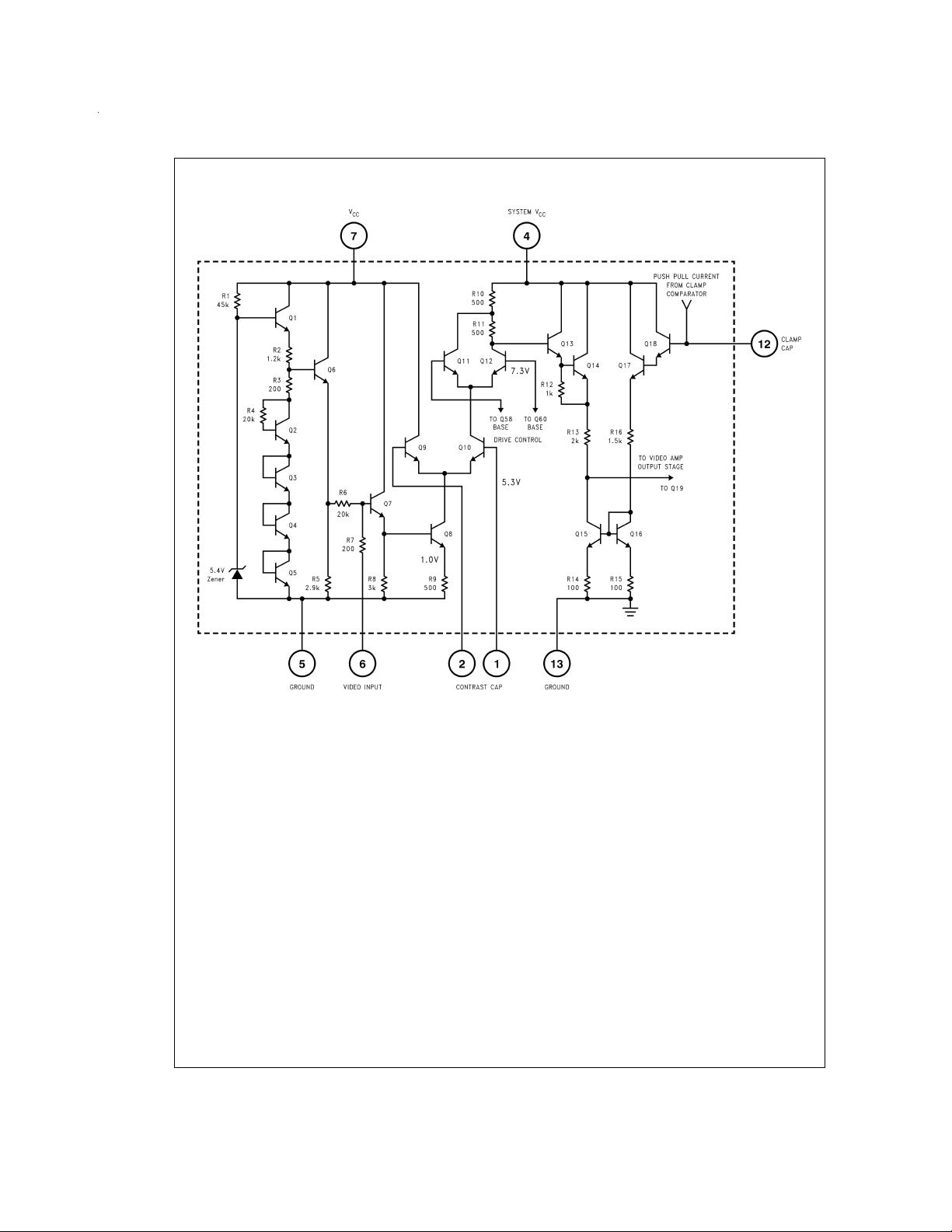
VIDEO AMPLIFIER SECTION (Input Stage)
A simplified schematic of LM2202’s video amplifier input
stage is shown in
Figure 3
. The 5.4V zener diode, Q1, Q6
and R2 bias the base of Q7 at 2.6V. The AC coupled video
Figure 2
). When the
signal applied to pin 6 is referenced to the 2.6V bias voltage.
Transistor Q7 buffers the video signal, V
the voltage to current. The AC collector current through Q8 is
=
I
/R9. Under maximum gain condition, transistors Q9
V
C8
IN
and Q11 are off and all of I
R10 and R11. The maximum signal gain at the base of Q13
=
is, A
achieved by varying the base drive to the differential pairs
−(R10 + R11)/R9=−2. Signal attenuation is
V1
flows through the load resistors
C8
, and Q8 converts
IN
Q9, Q10 and Q11, Q12 thereby unbalancing the collector
currents through the transistor pairs. Base of Q10 is biased
at 5.3V by externally connecting pin 1 to pin 20 through a
100Ω resistor. Pin 2 is connected to pin 3 through a 100Ω resistor.Adjustingthe contrast voltage at pin 8 produces a control voltage at pin 3 which drives the base of Q9. By varying
the voltage at the base of Q9, Q8’s collector current (I
diverted away from the load resistors R10 and R11, thereby
)is
C8
providing signal attenuation. Maximum attenuation is
achieved when all of I
flows through the load resistors.
flows through Q9 and no current
C8
The differential pair Q11 and Q12 provide drive control.
Q12’s base is internally biased at 7.3V.Adjusting the voltage
at the drive control input (pin 9) produces a control voltage at
the base of Q11. With Q9 off and Q12 off, all of I
through R10, thus providing a gain of A
=
−1. Drive control thus provides a 6 dB attenuation range.
=
−(R10/R9) x V
V1
flows
C8
IN
FIGURE 2. Block Diagram of the LM2202 Video Amplifier
with Contrast and Brightness (Black Level) Control
DS012591-8
www.national.com5
Circuit Description (Continued)
FIGURE 3. Simplified Schematic of the LM2202 Video Amplifier Input Stage
VIDEO AMPLIFIER SECTION (Output Stage)
A simplified schematic of LM2202’s video amplifier output
Figure 4
stage is shown in
gain stage. Ideally the gain of the second gain stage would
=
be A
low open loop gain, the gain is approximately A
Thus the maximum gain of the video amplifier is A
A
to the load. The output voltage can swing from 0.2V to 10V.
−R21/R18=−16. Because of the output stage’s
V2
=
20. Transistors Q23 and Q24 provide a push-pull drive
V2
. The output stage is the second
=
−10.
V2
=
A
V
V1
x
CONTRAST CONTROL SECTION
A simplified schematic of LM2202’s contrast control section
is shown in
Figure 5
. A 0V to 4V DC voltage is applied at the
contrast input (pin 8). Transistors Q29, Q30 and Q34 buffer
and level shift the contrast voltage to the base of Q36. The
voltage at the emitter of Q36 equals the contrast voltage
(V
) and the current through Q36’s collector is given by
cont
=
I
C36
/R28.
V
cont
Transistor Q36’s collector current is used to unbalance the
current through the differential pair comprised of Q38 and
Q40. Q40’s base is internally biased at 5.3V and made avail-
www.national.com 6
DS012591-9
able at pin 20. Pin 20 is externally connected to pin 1 through
a 100Ω resistor (see
Q38 (pin 3) is externally connected to pin 2 through a 100Ω
resistor (see
ferential pair (Q38, Q40) is balanced and the voltage at pins
Figure 2
Figure 2
and
Figure 3
and
). With V
Figure 3
). The base of
=
2V,the dif-
cont
1 and 2 is 5.3V. Under this condition, Q8’s collector current is
equally split between Q9 and Q10 (see
Figure 3
) and the
amplifier’s gain is half the maximum gain. If contrast voltage
at pin 8 is greater than 2V then Q36’s collector current increases, thus pulling Q38’s collector node lower and consequently moving Q38’s base below 5.3V.With pin 2 at a lower
voltage than pin 1, current through Q10 (see
creases and the amplifier’s gain increases. With V
the amplifier’s gain is maximum.
Figure 3
cont
=
) in-
4V,
If the contrast voltage at pin 8 is less than 2V then Q36’s collector current decreases and Q38’s base is pulled above
5.3V.With pin 2 voltage greater than pin 1 voltage, less current flows through Q10 (see
plifier’s gain decreases. With V
is minimum (i.e., maximum attenuation).
Figure 3
), consequently the am-
=
0V,the amplifier’s gain
cont
 Loading...