

LM20343
36V, 3A Adjustable Frequency Synchronous Buck
Regulator
LM20343 36V, 3A Adjustable Frequency Synchronous Buck Regulator
August 12, 2008
General Description
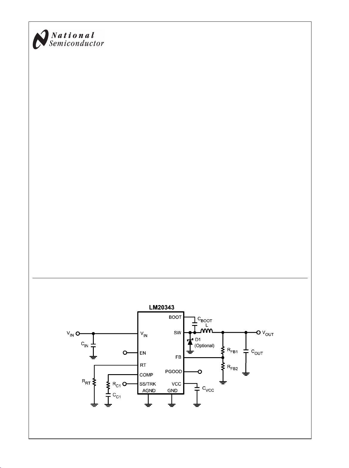
The LM20343 is a full featured synchronous buck regulator
capable of delivering up to 3A of load current. The current
mode control loop is externally compensated with only two
components, offering both high performance and ease of use.
The device is optimized to work over the input voltage range
of 4.5V to 36V making it well suited for high voltage systems.
The device features internal Over Voltage Protection (OVP)
and Over Current Protection (OCP) circuits for increased system reliability. A precision Enable pin and integrated UVLO
allows the turn on of the device to be tightly controlled and
sequenced. Startup inrush currents are limited by both an internally fixed and externally adjustable soft-start circuit. Fault
detection and supply sequencing are possible with the integrated power good (PGOOD) circuit.
The frequency of this device can be adjusted from 250 kHz to
1.0 MHz by connecting an external resistor from the RT pin
to ground.
The LM20343 is designed to work well in multi-rail power
supply architectures. The output voltage of the device can be
configured to track a higher voltage rail using the SS/TRK pin.
If the output of the LM20343 is pre-biased at startup it will not
sink current to pull the output low until the internal soft-start
ramp exceeds the voltage at the feedback pin.
The LM20343 is offered in an exposed pad 20-pin eTSSOP
package that can be soldered to the PCB, eliminating the
need for bulky heatsinks.
Features
4.5V to 36V input voltage range
■
3A output current, 5.2A peak current
■
130 mΩ/110 mΩ integrated power MOSFETs
■
94% peak efficiency with synchronous rectification
■
1.5% feedback voltage accuracy
■
Current mode control, selectable compensation
■
Resistor programmed, 1MHz capable oscillator
■
Adjustable output voltage down to 0.8V
■
Compatible with pre-biased loads
■
Programmable soft-start with external capacitor
■
Precision enable pin with hysteresis
■
OVP, UVLO inputs and PGOOD output
■
Internally protected with peak current limit, thermal
■
shutdown and restart
Accurate current limit minimizes inductor size
■
Non-linear current mode slope compensation
■
eTSSOP-20 exposed pad package
■
Applications
Simple to design, high efficiency point of load regulation
■
from a 4.5V to 36V bus
High Performance DSPs, FPGAs, ASICs and
■
Microprocessors
Communications Infrastructure, Automotive
■
Simplified Application Circuit
30051701
© 2008 National Semiconductor Corporation 300517 www.national.com
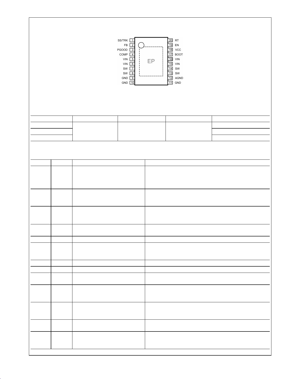
Connection Diagram
LM20343
Top View
eTSSOP-20 Package
30051702
Ordering Information
Order Number Package Type NSC Package Drawing Package Marking Supplied As
LM20343MH eTSSOP-20 MXA20A 20343MH 73 Units per Rail
LM20343MHE 250 Units per Tape and Reel
LM20343MHX 2500 Units per Tape and Reel
Pin Descriptions
Pin(s) Name Description Application Information
1 SS/TRK Soft-Start or Tracking control input An internal 4.5 µA current source charges an external capacitor to set
the soft-start rate. The PWM can track to an external voltage ramp with
a low impedance source. If left open, an internal 1 ms SS ramp is
activated.
2 FB Feedback input to the error amplifier
from the regulated output
3 PGOOD Power good output signal Open drain output indicating the output voltage is regulating within
4 COMP Output of the internal error amplifier and
input to the Pulse Width Modulator
5,6,15,16 VIN Input supply voltage Nominal operating range: 4.5V to 36V.
7,8,13,14 SW Switch pin The drain terminal of the internal Synchronous Rectifier power
9,10,11 GND Ground Internal reference for the power MOSFETs.
12 AGND Analog ground Internal reference for the regulator control functions.
17 BOOT Boost input for bootstrap capacitor An internal diode from VCC to BOOT charges an external capacitor
18 VCC Output of the high voltage linear
regulator. The VCC voltage is regulated
to approximately 5.5V.
19 EN Enable or UVLO input An external voltage divider can be used to set the line undervoltage
20 RT Internal oscillator frequency adjust input Normally biased at 550 mV. An external resistor connected between
EP Exposed
Pad
Exposed pad Exposed metal pad on the underside of the package with a weak
This pin is connected to the inverting input of the internal
transconductance error amplifier. An 800 mV reference is internally
connected to the non-inverting input of the error amplifier.
tolerance. A pull-up resistor of 10 kΩ to 100 kΩ is recommended if this
function is used.
The loop compensation network should be connected between the
COMP pin and the AGND pin.
NMOSFET and the source terminal of the internal Control power
NMOSFET.
required from SW to BOOT to power the Control MOSFET gate driver.
VCC tracks VIN up to about 7.2V. Above VIN = 7.2V, VCC is regulated
to approximately 5.5 Volts. A 0.1 µF to 1 µF ceramic decoupling
capacitor is required. The VCC pin is an output only.
lockout threshold. If the EN pin is left unconnected, a 2 µA pull-up
current source pulls the EN pin high to enable the regulator.
RT and AGND sets the internal oscillator frequency.
electrical connection to GND. Connect this pad to the PC board ground
plane in order to improve heat dissipation.
www.national.com 2
LM20343
Absolute Maximum Ratings (Note 1)
If Military/Aerospace specified devices are required,
please contact the National Semiconductor Sales Office/
Distributors for availability and specifications.
VIN to GND -0.3V to +38V
BOOT to GND -0.3V to +43V
BOOT to SW -0.3V to +7V
SW to GND -0.5V to +38V
VCC to GND -0.3V to +8V
Storage Temperature -65°C to 150°C
ESD Rating
Human Body Model (Note 2) 2kV
Operating Ratings
VIN to GND +4.5V to +36V
Junction Temperature −40°C to + 125°C
SW to GND (Transient) -1.5V (< 20 ns)
FB, EN, SS/TRK, RT,
-0.3V to +6V
PGOOD to GND
Electrical Characteristics Unless otherwise stated, the following conditions apply: V
= 12V. Limits in standard
VIN
type are for TJ = 25°C only, limits in bold face type apply over the junction temperature (TJ) range of -40°C to +125°C. Minimum
and Maximum limits are guaranteed through test, design, or statistical correlation. Typical values represent the most likely
parametric norm at TJ = 25°C, and are provided for reference purposes only.
Symbol Parameter Conditions Min Typ Max Units
V
FB
R
HSW-DS(ON)
R
LSW-DS(ON)
I
Q
I
SD
V
UVLO
V
UVLO(HYS)
V
VCC
I
SS
V
TRKACC
I
BOOT
V
F-BOOT
Feedback Pin Voltage V
= 4.5V to 36V 0.788 0.8 0.812 V
VIN
High-Side MOSFET On-Resistance ISW = 3A 130 225
Low-Side MOSFET On-Resistance ISW = 3A 110 190
Operating Quiescent Current V
= 4.5V to 36V 2.3 3 mA
VIN
Shutdown Quiescent Current VEN = 0V 150 180 µA
VIN Under Voltage Lockout Rising V
VIN
4 4.25 4.5 V
VIN Under Voltage Lockout Hysteresis 350 450 mV
VCC Voltage I
= -5 mA, VEN = 5V 5.5 V
VCC
Soft-Start Pin Source Current VSS = 0V 2 5 7 µA
Soft-Start/Track Pin Accuracy VSS = 0.4V -10 5 15 mV
BOOT Diode Leakage V
BOOT Diode Forward Voltage I
= 4V 10 nA
BOOT
= -100 mA 0.9 1.1 V
BOOT
Powergood
V
FB(OVP)
V
FB(OVP-HYS)
V
FB(PG)
V
FB(PG-HYS)
T
PGOOD
I
PGOOD(SNK)
I
PGOOD(SRC)
Over Voltage Protection Rising Threshold V
Over Voltage Protection Hysteresis
PGOOD Threshold, V
Rising V
OUT
PGOOD Hysteresis
Δ
ΔV
FB(OVP)
VFB(OVP)
/ V
FB(PG)
FB(PG)
/ V
/ V
/ V
FB
FB
FB
FB
107 110 112 %
2 3 %
93 95 97 %
2 3 %
PGOOD Delay 20 µs
PGOOD Low Sink Current V
PGOOD High Leakage Current V
= 0.5V 0.6 1 mA
PGOOD
= 5V 5 200 nA
PGOOD
Oscillator
F
SW1
F
SW2
D
MAX
V
RT
Switching Frequency 1
Switching Frequency 2
Maximum Duty Cycle I
RT pin voltage
RRT = 49.9 kΩ
RRT = 249 kΩ
= 3A 80 %
LOAD
RRT = 249 kΩ
675 750 825 kHz
225 250 325 kHz
550 mV
Error Amplifier
I
FB
I
COMP(SRC)
I
COMP(SNK)
g
m
A
VOL
Feedback Pin Bias Current VFB = 1V 50 nA
COMP Output Source Current VFB = 0V
V
= 0V
COMP
COMP Output Sink Current VFB = 1.6V
V
= 1.6V
COMP
Error Amplifier DC Transconductance I
= -50 µA to +50 µA 450 515 600 µmho
COMP
200 400 µA
200 350 µA
Error Amplifier Voltage Gain COMP pin open 2000 V/V
GBW Error Amplifier Gain-Bandwidth Product COMP pin open 7 MHz
mΩ
mΩ
3 www.national.com
Symbol Parameter Conditions Min Typ Max Units
Current Limit
LM20343
I
LIM
I
LIMNEG
T
ILIM
Cycle By Cycle Positive Current Limit 4.3 5.2 6.0 A
Cycle By Cycle Negative Current Limit 2.8 A
Cycle By Cycle Current Limit Delay 150 ns
Enable
V
EN(RISING)
V
EN(HYS)
I
EN
EN Pin Rising Threshold 1.2 1.25 1.3 V
EN Pin Hysteresis 50 mV
EN Source Current VEN = 0V, V
= 12V 2 µA
VIN
Thermal Shutdown
T
T
SD(HYS)
SD
Thermal Shutdown 170 °C
Thermal Shutdown Hysteresis 20 °C
Thermal Resistance
θ
JC
θ
JA
Note 1: Absolute Maximum Ratings indicate limits beyond witch damage to the device may occur. Operating Ratings indicate conditions for which the device is
intended to be functional, but do not guarantee specific performance limits. For guaranteed specifications and test conditions, see the Electrical Characteristics.
Note 2: The human body model is a 100 pF capacitor discharged through a 1.5 kΩ resistor to each pin.
Note 3: Measured on a 4 layer 2" x 2" PCB with 1 oz. copper weight inner layers and 2 oz. outer layers.
Junction to Case 5.6 °C/W
Junction to Ambient (Note 3) 0 LFM airflow 27 °C/W
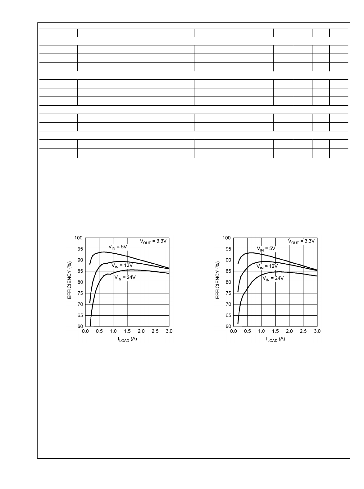
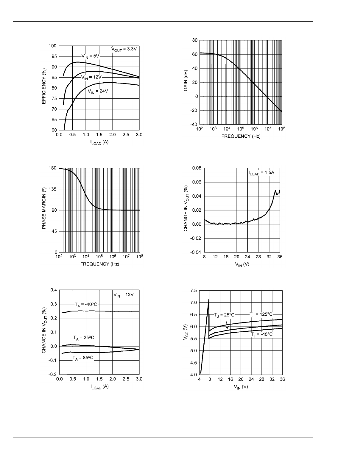
Typical Performance Characteristics Unless otherwise specified: V
= 12V, V
VIN
= 3.3V, L= 4.7µH,
OUT
fSW=750kHz, CSS= 100nF, TA = 25°C for efficiency curves, loop gain plots and waveforms, and TJ = 25°C for all others.
Efficiency vs. Load Current
fSW = 350 kHz
30051703
Efficiency vs. Load Current
fSW = 500 kHz
30051704
www.national.com 4
LM20343
Efficiency vs. Load Current
fSW = 750 kHz
Error Amplifier Phase
Error Amplifier Gain
30051705
30051785
Line Regulation
Load Regulation
30051706
30051786
30051707
VCC vs. V
IN
30051708
5 www.national.com
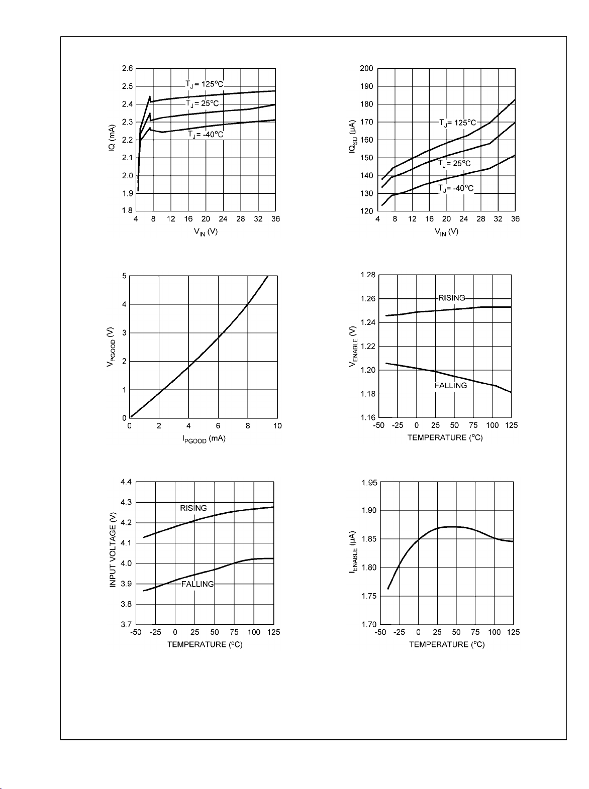
LM20343
Non-Switching IQ vs. V
IN
Shutdown IQ vs. V
IN
30051709
PGOOD Output Low Level Voltage vs. I
PGOOD
30051719
UVLO Threshold and Hysteresis vs. Temperature
30051710
EN Threshold and Hysteresis vs. Temperature
30051721
EN Current vs. Temperature
30051795
www.national.com 6
30051722
 Loading...