

现货库存、技术资料、百科信息、热点资讯,精彩尽在鼎好!
LM1894
Dynamic Noise Reduction System DNR
General Description
The LM1894 is a stereo noise reduction circuit for use with
audio playback systems. The DNR system is
non-complementary, meaning it does not require encoded
source material. The system is compatible with virtually all
prerecorded tapes and FM broadcasts. Psychoacoustic
masking, andan adaptive bandwidth scheme allow the DNR
to achieve 10 dB of noise reduction. DNR can save circuit
board space and cost because of the few additional components required.
Features
n Non-complementary noise reduction, “single ended”
n Low cost external components, no critical matching
LM1894 Dynamic Noise Reduction System DNR
December 1994
®
n Compatible with all prerecorded tapes and FM
n 10 dB effective tape noise reduction CCIR/ARM
weighted
n Wide supply range, 4.5V to 18V
n 1 Vrms input overload
Applications
n Automotive radio/tape players
n Compact portable tape players
n Quality HI-FI tape systems
n VCR playback noise reduction
n Video disc playback noise reduction
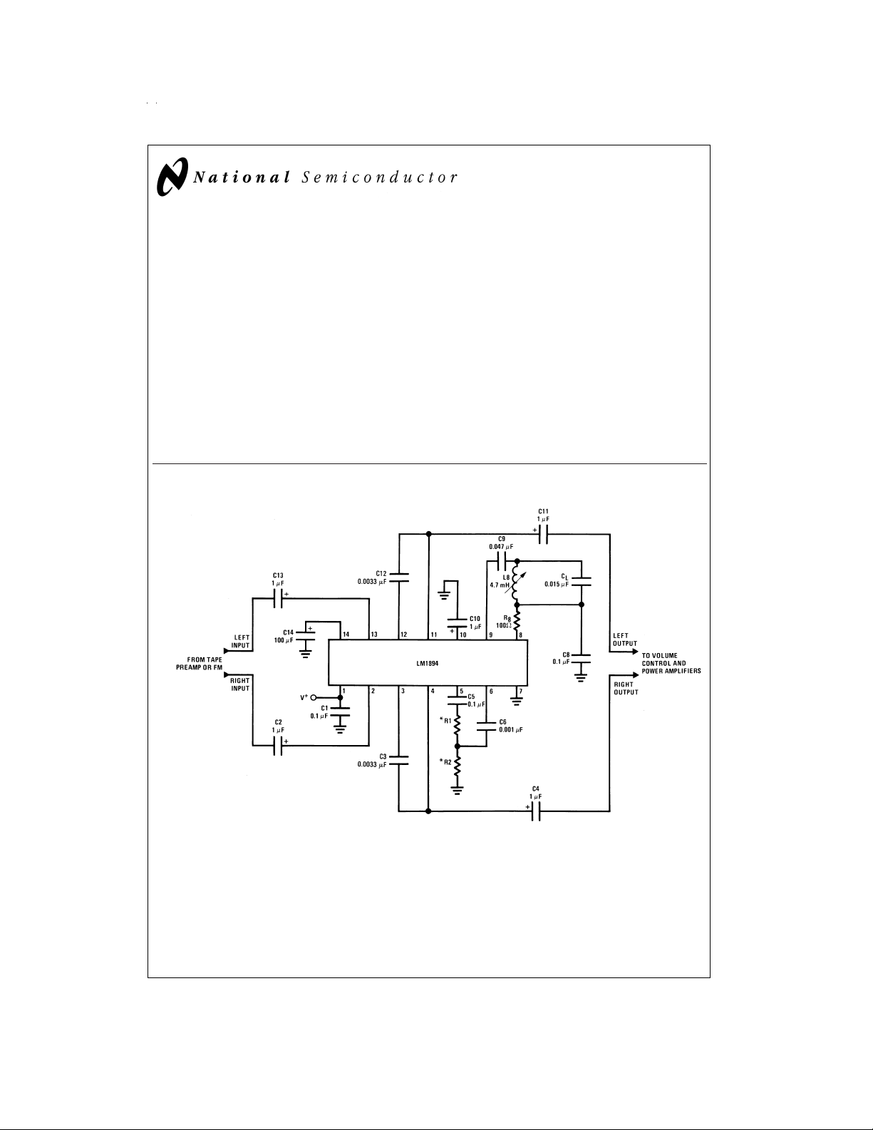
Typical Application
*R1+R2=1kΩtotal.
See Application Hints.
DS007918-1
Order Number LM1894M or LM1894N
See NS Package Number M14A or N14A
FIGURE 1. Component Hook-Up for Stereo DNR System
DNR®is a registered trademark of National Semiconductor Corporation.
®
The DNR
system is licensed to National Semiconductor Corporation under U.S. patent 3,678,416 and 3,753,159.
Trademark and license agreement required for use of this product.
© 1999 National Semiconductor Corporation DS007918 www.national.com
Absolute Maximum Ratings (Note 1)
If Military/Aerospace specified devices are required,
please contact the National Semiconductor Sales Office/
Distributors for availability and specifications.
Supply Voltage 20V
Input Voltage Range, V
pk
Operating Temperature (Note 2) 0˚C to +70˚C
Storage Temperature −65˚C to +150˚C
Soldering Information
Dual-In-Line Package
Soldering (10 seconds) 260˚C
VS/2
Small Outline Package
Vapor Phase (60 seconds) 215˚C
Infrared (15 seconds) 220˚C
See AN-450 “Surface Mounting Methods and Their Effect
on Product Reliability” for other methods of soldering
surface mount devices.
Note 1: “Absolute Maximum Ratings” indicate limits beyond which damage
to the device may occur. Operating Ratings indicate conditions for which the
device is functional, but do not guarantee specific performance limits.
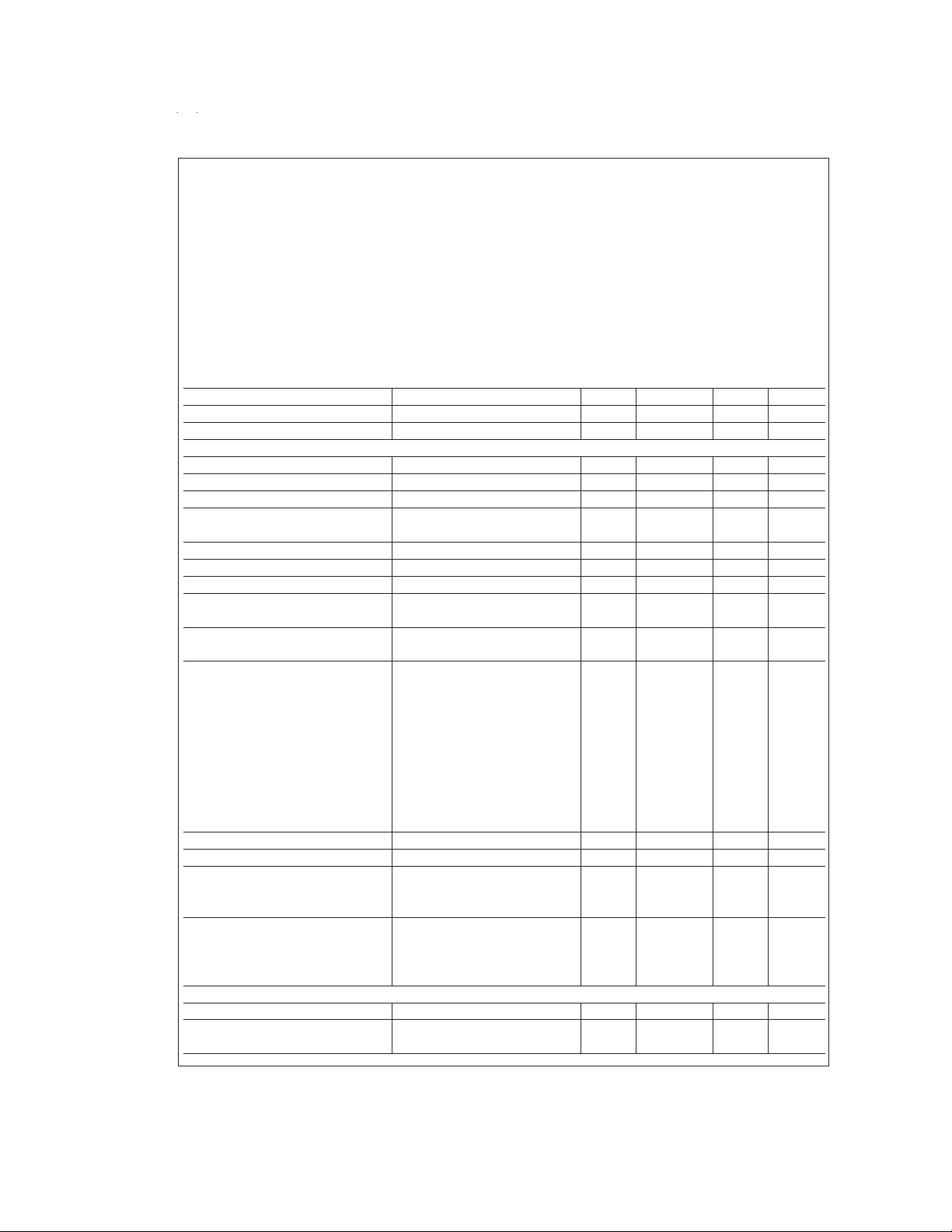
Electrical Characteristics
=
V
S
Operating Supply Range 4.5 8 18 V
Supply Current V
MAIN SIGNAL PATH
Voltage Gain DC Ground Pin 9, (Note 3) −0.9 −1 −1.1 V/V
DC Output Voltage 3.7 4.0 4.3 V
Channel Balance DC Ground Pin 9 −1.0 1.0 dB
Minimum Balance AC Ground Pin 9 with 0.1 µF 675 965 1400 Hz
Maximum Bandwidth DC Ground Pin 9, (Note 3) 27 34 46 kHz
Effective Noise Reduction CCIR/ARM Weighted, (Note 4) −10 −14 dB
Total Harmonic Distortion DC Ground Pin 9 0.05 0.1
Input Headroom Maximum V
Output Headroom Maximum V
Signal to Noise BW=20 Hz–20 kHz, re 300 mV
Input Impedance Pin 2 and Pin 13 14 20 26 kΩ
Channel Separation DC Ground Pin 9 −50 −70 dB
Power Supply Rejection C14=100 µF,
Output DC Shift Reference DVM to Pin 14 and
CONTROL SIGNAL PATH
Summing Amplifier Voltage Gain Both Channels Driven 0.9 1 1.1 V/V
Gain Amplifier Input Impedance
Voltage Gain
8V, T
A
=
25˚C, V
=
300 mV at 1 kHz, circuit shown in
IN
Figure 1
unless otherwise specified
Parameter Conditions Min Typ Max Units
=
8V 17 30 mA
S
Capacitor, (Note 3)
for 3%THD 1.0 Vrms
IN
AC Ground Pin 9
for 3%THD VS− 1.5 Vp-p
OUT
DC Ground Pin 9
AC Ground Pin 9 79 dB
DC Ground Pin 9 77 dB
CCIR/ARM Weighted re 300 mV
(Note 5)
AC Ground Pin 9 82 88 dB
DC Ground Pin 9 70 76 dB
CCIR Peak, re 300 mV, (Note 6)
AC Ground Pin 9 77 dB
DC Ground Pin 9 64 dB
=
V
500 mVrms, −40 −56 dB
RIPPLE
f=1 kHz
Measuree Output DC Shift from 4.0 20 mV
Minimum to Maximum Bandwidth, (Note 7).
Pin6 243039kΩ
Pin 6 to Pin 8 21.5 24 26.5 V/V
%
www.national.com 2

Electrical Characteristics (Continued)
=
V
S
CONTROL SIGNAL PATH
Peak Detector Input Impedance Pin 9 560 700 840 Ω
Voltage Gain Pin 9 to Pin 10 30 33 36 V/V
Attack Time Measured to 90%of Final Value 300 500 700 µs
Decay Time Measured to 90%of Final Value 45 60 75 ms
DC Voltage Range Minimum Bandwidth to Maximum 1.1 3.8 V
Note 2: For operation in ambient temperature above 25˚C,the device must be derated based on a 150˚C maximum junction temperature and a thermal resistance
of 1) 80˚C/W junction to ambient for the dual-in-line package, and 2) 105˚C/W junction to ambient for the small outline package.
Note 3: To force the DNR system intomaximum bandwidth, DC ground the input to the peak detector, pin9. A negative temperature coefficientof −0.5%/˚C on the
bandwidth, reduces the maximum bandwidth at increased ambienttemperatureorhigherpackage dissipation.ACground pin 9 or pin 6 to select minimum bandwidth.
To change minimum and maximum bandwidth, see Appliction Hints.
Note 4: The maximum noise reduction CCIR/ARM weighted is about14 dB. This isaccomplished by changing the bandwidth from maximum to minimum. In actual
operation, minimum bandwidth is not selected, a nominal minimum bandwidth of about 2 kHz gives −10 dB of noise reduction. See Application Hints.
Note 5: The CCIR/ARM weighted noise is measured with a 40 dB gain amplifier between the DNR system and the CCIR weighting filter; it is then input referred.
Note 6: Measured using the Rhode-Schwartz psophometer.
Note 7: Pin 10 is DC forced half way between the maximum bandwidth DC level and minimum bandwidth DC level. An AC 1 kHz signal is then applied to pin 10.
Its peak-to-peak amplitude is V
8V, T
A
=
25˚C, V
=
300 mV at 1 kHz, circuit shown in
IN
Figure 1
unless otherwise specified
Parameter Conditions Min Typ Max Units
with 10 kHz Tone Burst
with 10 kHz Tone Burst
Bandwidth
(max BW) − VDC(min BW).
DC
Typical Performance Characteristics
Supply Current vs
Supply Voltage
THD vs Frequency
DS007918-13
DS007918-16
Channel Separation
(Referred to the Output)
vs Frequency
−3 dB Bandwidth
vs Frequency and
Control Signal
DS007918-14
DS007918-17
Power Supply Rejection
Ratio (Referred to the
Output) vs Frequency
DS007918-15
Gain of Control Path
vs Frequency (with
10 kHz FM Pilot Filter)
DS007918-18
www.national.com3
 Loading...