

现货库存、技术资料、百科信息、热点资讯,精彩尽在鼎好!
LM1893/LM2893 Carrier-Current Transceiver
April 1995
LM1893/LM2893 Carrier-Current Transceiver
General Description
Carrier-current systems use the power mains to transfer information between remote locations. This bipolar carriercurrent chip performs as a power line interface for half-duplex (bi-directional) communication of serial bit streams of
virtually any coding. In transmission, a sinusoidal carrier is
FSK modulated and impressed on most any power line via a
rugged on-chip driver. In reception, a PLL-based demodulator and impulse noise filter combine to give maximum range.
A complete system may consist of the LM1893, a COPS
controller, and discrete components.
Features
Y
Noise resistant FSK modulation
Y
User-selected impulse noise filtering
Y
Up to 4.8 kBaud data transmission rate
Y
Strings of 0’s or 1’s in data allowed
Y
Sinusoidal line drive for low RFI
Typical Application
Y
Output power easily boosted 10-fold
Y
50 to 300 kHz carrier frequency choice
Y
TTL and MOS compatible digital levels
Y
Regulated voltage to power logic
Y
Drives all conventional power lines
Applications
Y
Energy management systems
TM
Y
Home convenience control
Y
Inter-office communication
Y
Appliance control
Y
Fire alarm systems
Y
Security systems
Y
Telemetry
Y
Computer terminal interface
²
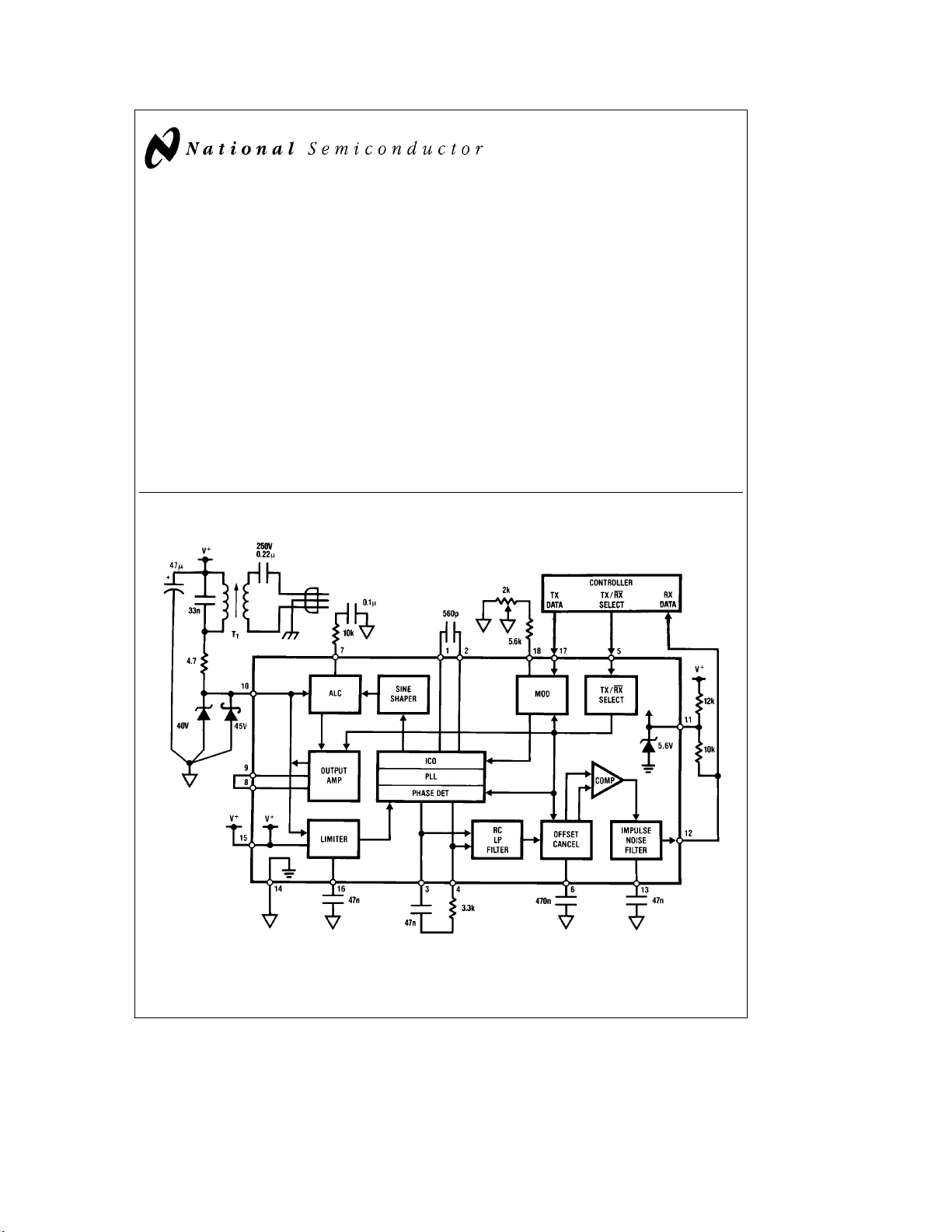
FIGURE 1. Block diagram of carrierÐcurrent chip with a complement of discrete components making a complete
e
F
125 kHz, f
O
BI-LINETMand COPSTMare trademarks of National Semiconductor Corp.
²
Carrier-Current Transceivers are also called Power Line Carrier (PLC) transceivers.
C
1995 National Semiconductor Corporation RRD-B30M115/Printed in U. S. A.
e
360 Baud transceiver. Use caution with this circuitÐdangerous line voltage is present.
DATA
TL/H/6750
TL/H/6750– 1
Absolute Maximum Ratings
If Military/Aerospace specified devices are required,
please contact the National Semiconductor Sales
Office/Distributors for availability and specifications.
Supply voltage 30 V
Voltage on pin 12 55 V
Voltage on pin 10 (Note 1) 41 V
Voltage on pins 5 and 17 40 V
5.6 V DC zener current 100 mA
Junction temperature: transmit mode 150
Electro-Static Discharge (120 pF, 1500X) 1KV
receive mode 125
Maximum continuous dissipation, T
plastic DIP N (Note 2): transmit mode 1.66 W
Operating ambient temp. range
Storage temperature range
Lead temp., soldering, 7 seconds 260
Absolute maximum ratings indicate limits beyond
Note:
which damage to the device may occur. Electrical specifications are not ensured when operating the device above
C
§
§
guaranteed limits but below absolute maximum limits, but
C
there will be no device degradation.
receive mode 1.33 W
e
25§C,
A
b
40 to 85§C
b
65 to 150§C
C
§
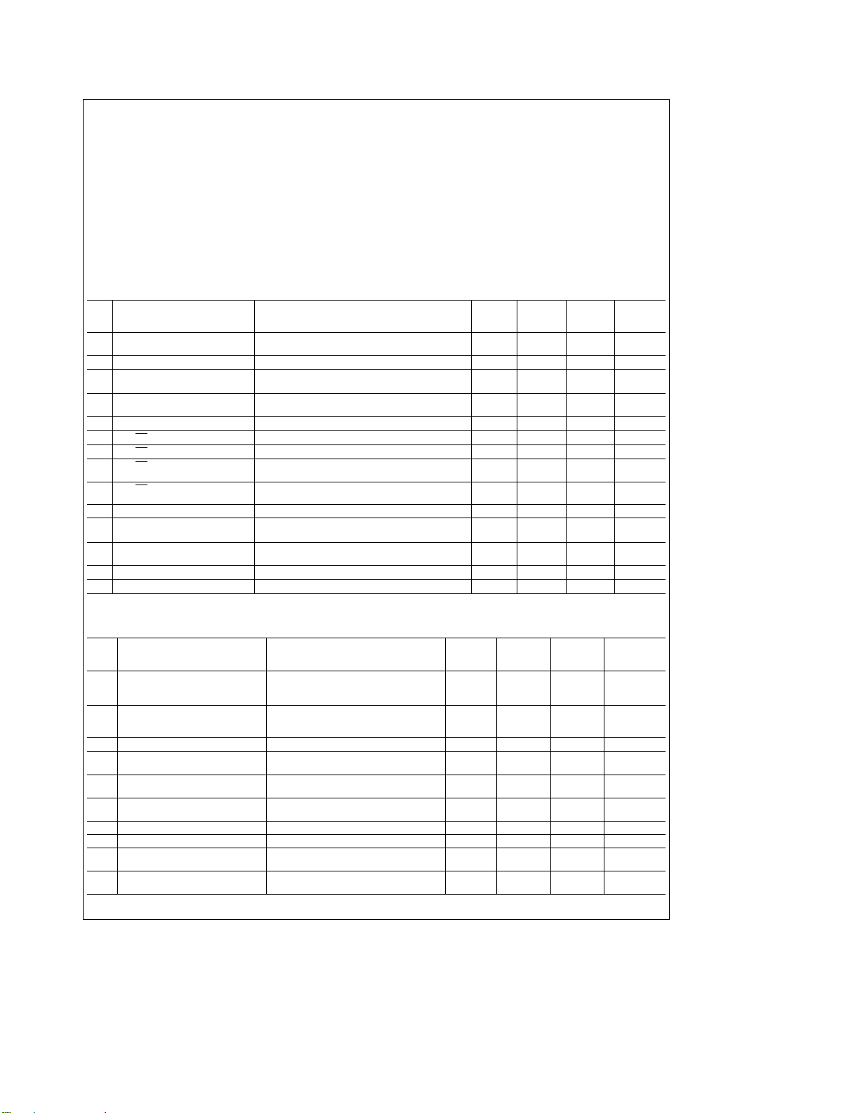
General Electrical Characteristics
(Note 3). The test conditions are: V
Ý
1 5.6 V Zener voltage, V
Parameter Conditions Typical Limit Limit
Z
2 5.6 V Zener resistance, R
3 Carrier I/O peak survivable Pin 10, discharge 1 mF cap. charged to V
transient voltage, V
OT
4 Carrier I/O clamp voltage, V
5 Carrier I/O clamp resistance, R10Pin 10, I
6 TX/RX low input voltage, V
7 TX/RX high input voltage, V
8 TX/RX low input current, I
9 TX/RX high input current, I
10 RXbTX switch-over time, T
11 TXbRX switch-over time, T
12 ICO initial accuracy of F
O
13 ICO temperature coefficient of FOTX or RX mode, (F
14 Temperature drift of F
O
Transmitter Electrical Characteristics (Note 3). The test conditions are: V
unless otherwise noted. The transmit center frequency is F
Ý
15 Supply voltage, Va, range Meets test 17 spec. at T
16 Total supply current, I
17 Carrier I/O output current, I
18 Carrier I/O lower swing limit, V
19 THD of IO(Note 6) Q of 10 tank driving 10X line 0.6 5.0 % max.
20 FSK deviation, F
21 Data In. low input voltage, V
22 Data In. high input voltage, V
23 Data In. low input current, I
24 Data In. high input current, I
Parameter Conditions Typical Limit Limit
QT
b
F
2
1
a
e
18V and F
Pin 11, I
Z
Pin 11, R
thruk1X
Pin 10, I
OC
2N2222 diode pin 8 to 9 50 V max.
Pin 5 1.8 0.8 V max.
IL
Pin 5 (Note 9) 2.2 2.8 V min.
IH
IL
IH
Pin 5 at 0.8 V
Pin5at40V
Time to develop 63% of full current drive thru pin 10 10 ms
RT
1 bit time, T
TR
controlled with C
TX mode, R
e
F
0
TX or RX mode,b40sT
(F
l
(F
l
Pin 15. Pin 12 high. IQTis IQthrough 52 79 mA max.
pin 15 and the average current I
Carrier I/O through pin 10
O
100X load on pin 10 70 45 mApp min.
Pin 10. Set internally be ALC. 4.7 4.0 V min.
ALC
2N2222 diode pin 8 to 9 5.7 V max.
e
125 kHz, unless otherwise noted.
O
Test Design
(Note 4) (Note 5)
e
2 mA 5.6 5.2 V min.
Z
@
e
(V
10 mAbV
Z
Z
e
10 mA, RX mode 44 41 V min.
OC
e
10 mA 20 X
OC
e
1/(2F
B
M
e
6.65 kX,C
O
a
(F
F2)/2 137 kHz max.
1
@
1 mA)/(10 mAb1 mA) 5 X
Z
). Time TTRis user 2 bit
DATA
, see Apps. Info.
O
b
F
OMAX
OMIN
s
T
J
JMAX
, FSK low is F1, and FSK high is F2.
O
OT
e
560 pF 125 113 kHz min.
b
)/(T
T
JMAX
JMIN
80 60 V max.
b
b
10
b
)
100 PPM/§C
g
2.0
5.9 V max.
b
2
20 mA min.
1 mA max.
b
4
1 0 mA min.
10 mA max.
a
e
18 V and F
g
5.0 % max.
e
125 kHz
O
Test Design
(Note 4) (Note 5)
e
25§C and: 13 14 15 V min.
J
b
[
]
[
F
14V
[
24V
18V])/F
1
b
]
[
F
18V])/F
1
1
1
k
[
]
0.01 40 24 23 V max.
18V
l
1
k
[
]
0.01
18V
l
1
of the
ODC
Limit
Units
Limit
Units
100X load, no tank 5.5 9 % max.
b
a
(F
F1)/([F
2
IL
IH
IL
IH
Pin 17 1.7 0.8 V max.
Pin 17 (Note 9) 2.1 2.8 V min.
Pin 17 at 0.8 V
Pin 17 at 40 V
]
F
/2) 4.4 3.7 % min.
2
1
b
1
b
10
5.2 % max.
b
10 mA min.
1 mA max.
b
4
1 0 mA min.
10 mA max.
2
a
(Note 4) (Note 5)
40
45
e
Test Design
g
g
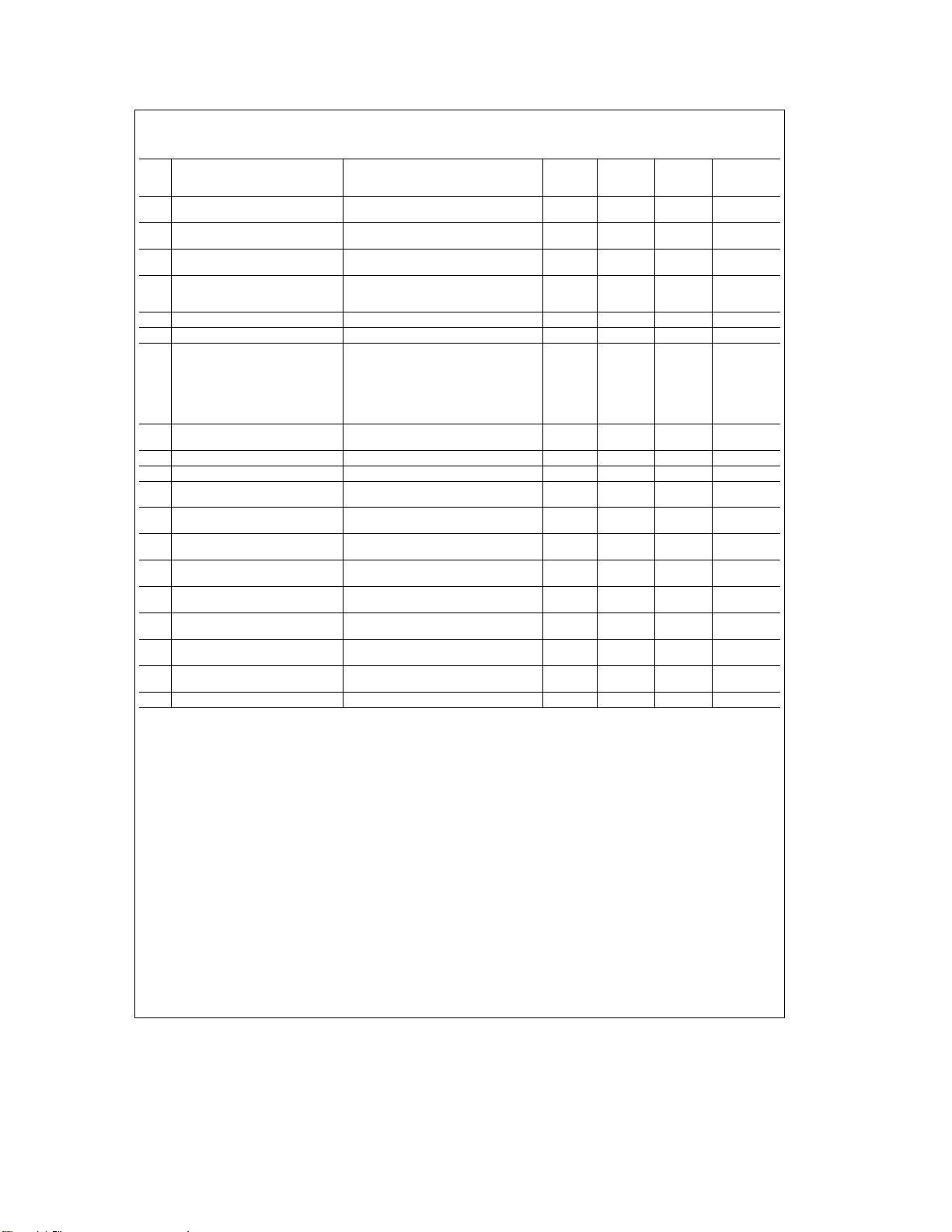
Receiver Electrical Characteristics (Note 3). The test conditions are: V
deviation FSK, F
Ý
25 Supply voltage, Va, range Functional receiver (Note 7) 12 13 13.5 V min.
26 Supply current, I
27 Carrier I/O input resistance, R
28 Max. data rate, F
29 PLL capture range, F
30 PLL lock range, F
31 Receiver input sensitivity, S
32 Tolerable input dc voltage offset Pin 10 lower than pin 15 by V
range, V
DATA
e
2.4 kHz, V
e
100 mVpp, in the receive mode, unless otherwise noted.
IN
Parameter Conditions Typical Limit Limit
37 30 28 V max.
QT
10
MD
C
L
IN
INDC
IQTis pin 15 (Va) plus pin 10 11 5 mA min.
(Carrier I/O) current. 2.4 kX Pin 13 to GND. 14 mA max.
Pin 10 19.5 14 kX min.
Functional receiver (Note 7), C
e
0X, no tank,
R
F
e
4.8 kBaud
2.4 kHz
e
C
F
e
C
F
For a functional receiver (Note 8)
Referred to chip side (pin 10) 1.8 10 12 mV
of the line-coupling XFMR: F
Referred to line side of XFMR: 0.26 mV
(assuming a 7.07:1 XFMR) F
100 pF, R
100 pF, R
e
0 X
F
e
0 X
F
e
100 pF, 10 4.8 2.4 kBaud
F
g
g
e
50 kHz 2.0 mV
O
e
F
300 kHz 1.4 mV
O
e
50 kHz 0.29 mV
O
e
F
300 kHz 0.20 mV
O
INDC
2 0.1 V max.
e
18 V, F
125 kHz,g2.2%
O
Limit
Units
30 kX max.
15
g
10 % min.
15 % min.
RMS
RMS
RMS
RMS
RMS
RMS
33 Data Out. breakdown voltage Pin 12, leakage Is20 mA 70 55 V min.
e
g
V
OH
e
2 mA 0.15 0.4 V max.
OL
g
55
g
45 mA min.
g
85 mA max.
3.5 V max.
e
g
250 mV
a
WINDOW
to above 2.8 V.
DC offset 0.95 0.70 V/V min.
g
55
b
0.5
C to insure that the junction temperature remains below the
§
(fundamental)].
RMS
DATA
g
25 mA min.
g
80 mA max.
b
20
e
1.2 kHz, (2) all of the data transitions must fall
b
40 nA min.
e
e
T
25§C. Pin
A
J
34 Data Out. low output, V
35 Impulse noise filter current, I
OL
I
36 Offset hold cap. bias voltage, V
37 Offset hold capacitor max. drive Pin 6. V(pin 3)bV(pin 4)
current, I
R
PD
voltage, V
-to-V
PD
MCM
PD
ratio, VW/V
OHB
PC
PD
38 Offset hold bias current, I
39 Phase comparator current, I
40 Phase detector output resistance, Pins 3 and 4. 10 6 kX min.
41 Phase detector demodulated output Pin 3 to 4, measured after filtering 100 60 mVpp min.
42 Fast offset cancel voltage ‘‘window’’ V
43 Power supply rejection, PSRR C
Note 1: More accurately, the maximum voltage allowed on pin 10 is VOC, and VOCranges from 41 to 50V. Also, transients may reach above 60V; see the transient
peak voltage characteristic curve.
Note 2: The maximum power dissipation rating should be derated for device operation above 25
maximum rating. Use a i
detail.
Note 3: The boldface values apply over the full junction temperature range for the specified supply voltage range. All other numbers apply at T
numbers refer to LM1893. LM2893 tested by shorting Carrier In to Carrier Out and testing it as an LM1893.
Note 4: Guaranteed and 100% production tested.
Note 5: Guaranteed (but not 100% production tested) over the temperature and supply voltage ranges. These limits are not used to calculate outgoing quality
levels.
Note 6: Total harmonic distortion is measured using THD
Note 7: Receiver function is defined as the error-free passage of 1 cycle of 50% duty-cycle 2.4 kHz square-wave data (2 sequential 208 mS bits), with the first bit
being a ‘‘1.’’ All of the data transitions (edges) must fall within
filter cap. C
Note 8: During the sensitivity check, note 7 requirements are followed with these exceptions: (1) data rate F
within
approximately 6200 pF).
Note 9: For TTL compatibility use a pull-up resistor to increase min. V
for this test.
I
g
20% (g41.6 ms) of their noise-free positions, and (3), a time-domain filter capacitor (CI) is used. The time delay of CIis (/2 bit, or 208 ms. (CIis
of 75§C/W for the N package using a socket in still air (which is the worst case). Consult the Application Information section for more
JA
Pin 12, sat. voltage at I
Pin 13 charge and discharge current
Pin 6 2.0 1.3 V min.
CM
Pin 6, TX mode. Bias pin 6 as it selfbiased during test 31. 40 nA max.
Bias pins 3 and 4 at 8.5 V 100 50 mA min.
e
I
I(pin 3)aI(pin 4), TX mode 200 mA max.
PC
e
R
(V@100mAbV@50mA)/(50mA) 18 kX max.
PD
out the 2FOcomponent 180 mVpp max.
b
V
PIN3
PIN4
Drive forg1 mA pin 6 current 1.20 V/V max.
e
0.1 mF. PSRReCMRR. 120 Hz 80 dB min.
L
e
[
(all components at or above 2FO)]/[I
I
RMS
g
10% (g20.8 ms) of their noise-free positions. RX time delay is minimized by using no impulse noise
3
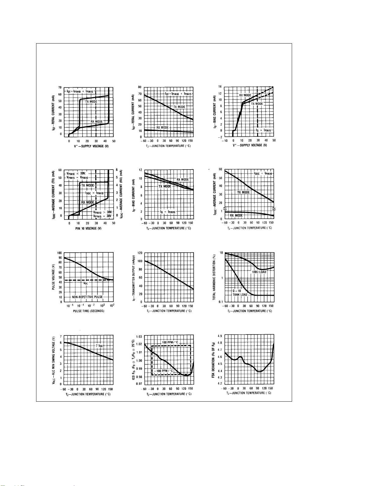
Typical Performance Characteristics (V
LM1893)
a
e
18V, F
e
125 kHz, circuit of
O
Figure 1
, pin numbers for
Total Current Consumption,
, vs Supply Voltage
I
QT
Chip Bias Current, I
vs Junction Tempurature
,
Q
Transient Voltage Survival
vs Pulse Time
Total Current Consumption,
IQT, vs Junction Temperature
Output Stage DC Current,
I
, vs Output Voltage
ODC
Transmitter AC Output Current
vs Junction Temperature
Chip Bias Current,
iQ, vs Supply Voltage
Output Stage DC Current,
I
,vs
ODC
Junction Temperature
Transmitter Sinusoid THD
vs Junction Temperature
ALC Voltage vs
Junction Temperature
ICO Frequency vs
Junction Temperature
4
Transmitter FSK Deviation
vs Junction Temperature
TL/H/6750– 38
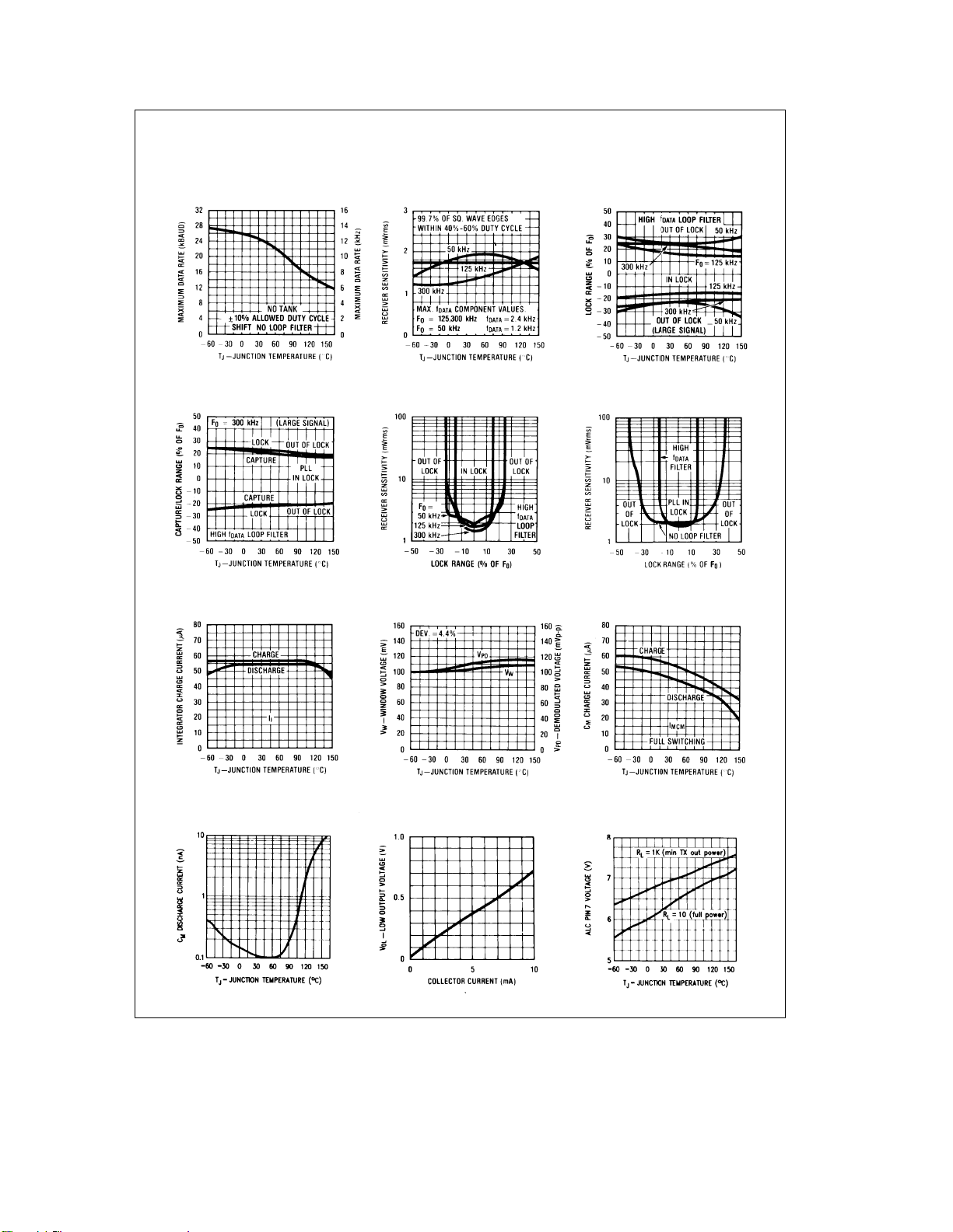
Typical Performance Characteristics (Continued)
Maximum Data Rate vs
Junction Temperature
PLL Capture & Lock Range vs
Junction Temperature
Impulse Noise Filter
Current vs Junction
Temperature
Receiver Sensitivity vs
Junction Temperature
Receiver Sensitivity vs
PLL Lock Range and F
Phase Detector Output
Voltage vs Junction
Temperature
PLL Lock Range vs
Junction Temperature and F
Receiver Sensitivity vs
O
PLL Lock Range and Loop Filter
Offset Hold Cap. Charge
Currents vs Junction
Temperature
O
Offset Hold Cap. Bias Current vs
Junction Temperature
Data Out. Low Voltage vs
Pull Down Current
5
Pin 7 Bias Voltage vs
Junction Temperature
TL/H/6750– 39
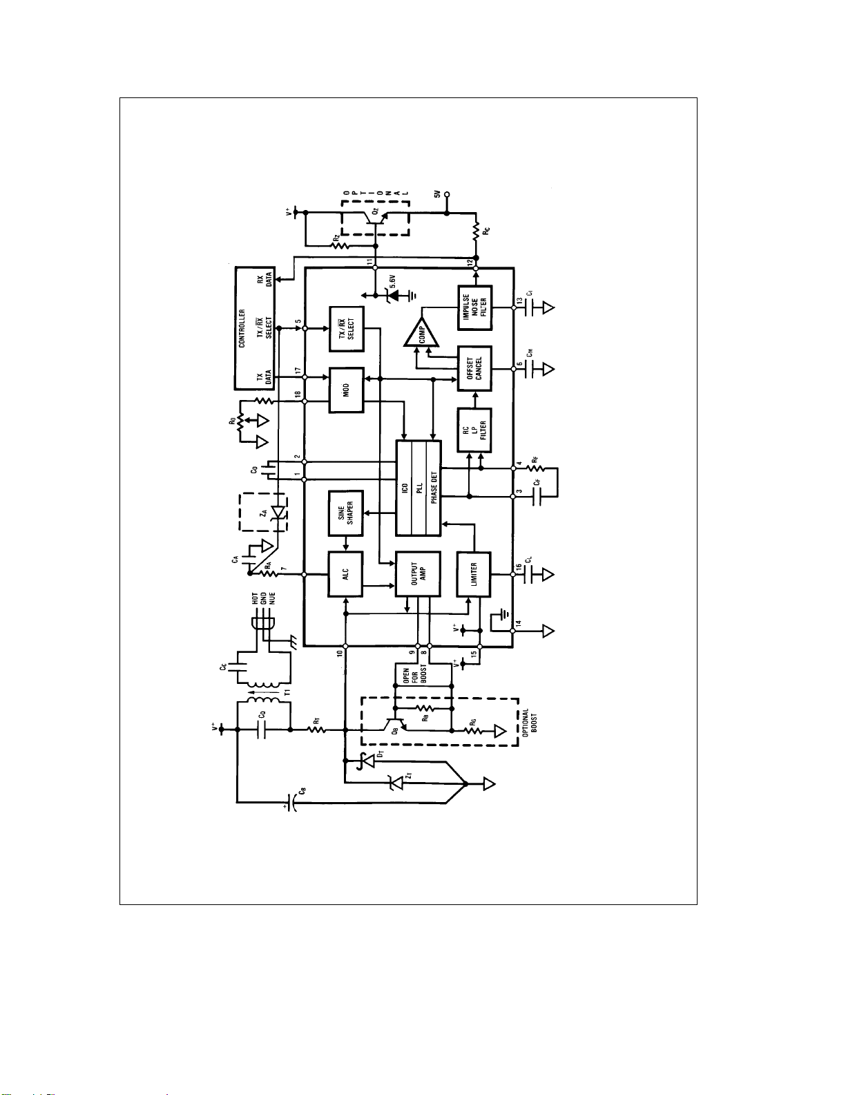
Application Information*
THE DATA PATH
The BI-LINETMchip serves as a power line interface in the
carrier-current transceiver (CCT) system of
4
shows the interface circuit now discussed. The controller
may select either the transmit (TX) or receive (RX) mode.
Serial data from the controller is used to generate a FSKmodulated 50 to 300 kHz carrier on the line in the TX mode.
In the RX mode line signal passes through the coupling
transformer into the PLL-based receiver. The recreated serial bit stream drives the controller.
With the IC in the TX mode (pin 5 a logic high), baseband
data to 5 kHz drive the modulator’s Data In pin to generate
a switched 0.978I/1.022I control current to drive the low TC,
triangle-wave, current-controlled oscillator to
tion. The tri-wave passes through a differential attenuator
and sine shaper which deliver a current sinusoid through an
automatic level control (ALC) circuit to the gain of 200 current output amplifier. Drive current from the Carrier I/O develops a voltage swing on T
proportional to line impedance, then passes through the
’s (
1
step-down transformer and coupling capacitor C
line. Progressively smaller line impedances cause reduced
signal swing, but never clipping-thus avoiding potential radio
frequency interference. When large line impedances threaten to allow excessive output swing on pin 10, the ALC
shunts current away from the output amplifier, holding the
voltage swing constant and within the amp’s compliance
limit. The amplifier is stable with a load of any magnitude or
phase angle.
In the RX mode (pin 5 a logic low), the TX sections on the
chip are disabled. Carrier signal, broad-band noise, transient
spikes, and power line component impinge of the receiver’s
input highpass filter, made up of C
bandpass filter. In-band carrier signal, band-limited noise,
heavily attenuated line frequency component, and attenuated transient energy pass through to produce voltage swing
on the tank, swinging about the positive supply to drive the
Carrier I/O receiver input. The balanced Norton-input limiter
amplifier removes DC offsets, attenuates line frequency,
performs as a bandpass filter, and limits the signal to drive
the PLL phase detector differentially. The differential demodulated output signal from the phase detector, containing AC and DC data signal, noise, system DC offsets, and a
large twice-the-carrier-frequency component, passes
through a 3-stage RC lowpass filter to drive the offset cancel circuit differentially. The offset cancelling circuit works
by insuring that the (fixed)
g
50 mV signal delivered to the
data squaring (‘‘slicing’’) comparator is centered around the
0 mV comparator switch point. Whenever the comparator
signal plus DC offset and noise moves outside the carefully
matched
g
50 mV voltage ‘‘window’’ of the offset cancel
circuit, it adjusts its DC correction voltage in series with the
differential signal to force the signal back into the window.
While the signal is within the
is stored on capacitor C
offset hold capacitor charging during offset cancelling, the
g
50 mV window, the DC offset
. By grace of the highly non-linear
M
DC cancellation is done much more quickly than with an AC
coupling capacitor normally used in place of the offset cancel circuit. Since impulse noise spikes normally ring the signal symmetrically around 0 V, the fully bilateral offset cancel
topology affords excellent noise rejection. The switched current output of the comparator drives the impulse noise filter
integrator capacitor that rejects all data pulses of less than
the integrator charge time. Noise appears as duty-cycle jitter
at the open collector serial data output.
Figure 3.Figure
g
2.2% devia-
Figure 4
) resonant tank
C
and T1, and the tank
C
onto the
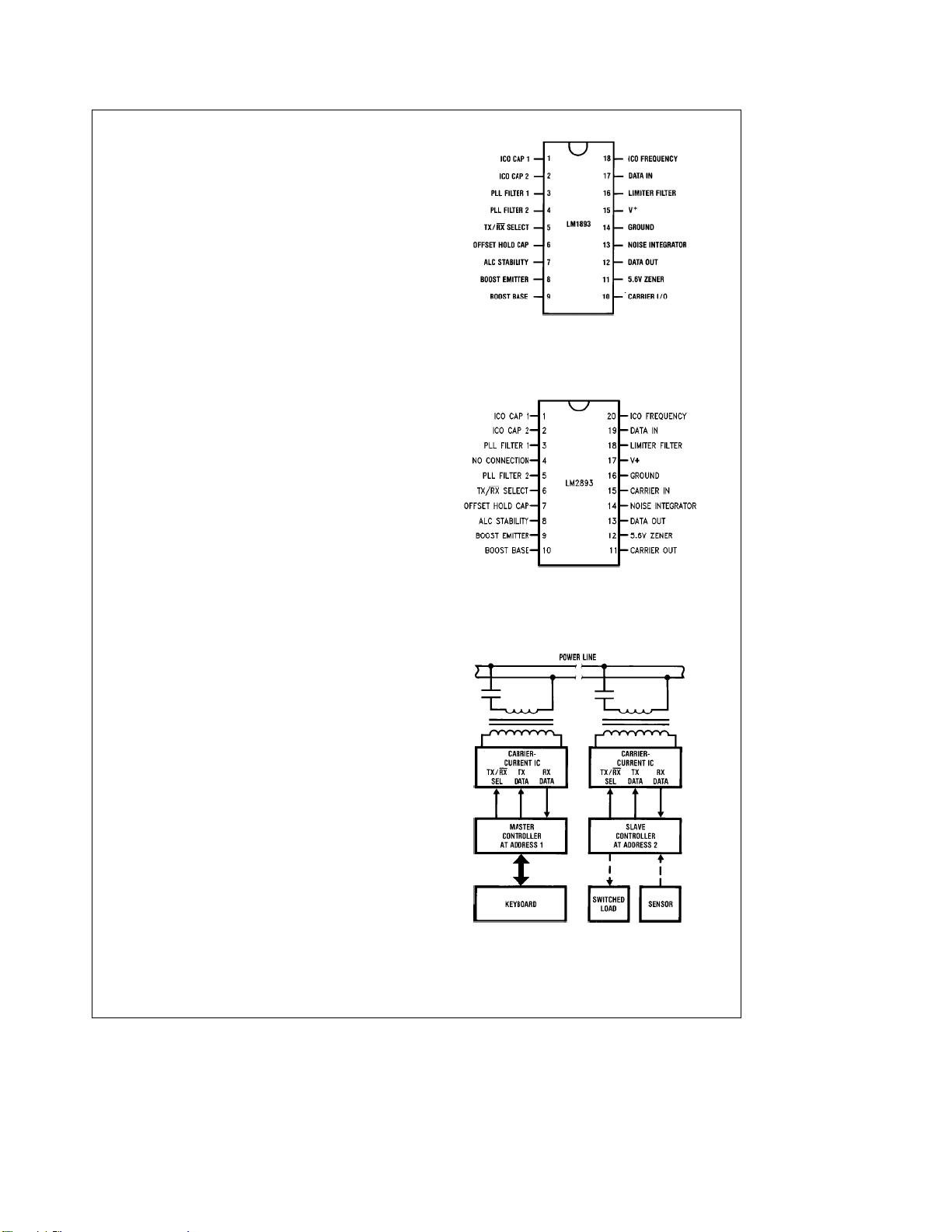
Dual-In-Line Package
Top View
Order Number LM1893N
See NS Package Number N18A
Small Outline & Dual-In-Line Package
Top View
Order Number LM2893M or LM2893N
See NS Package Number M20B or N20A
FIGURE 2. Connection Diagrams
FIGURE 3. The block diagram of a carrier-current
system using the Bi-Line chip to interface digital
controllers via the power line
*Unless otherwise noted, all pin references refer to LM1893, but hold true
for equivalent LM2893 pin.
6
TL/H/6750– 2
TL/H/6750– 41
TL/H/6750– 3
Application Information (Continued)
TL/H/6750– 4
FIGURE 4. Block diagram of a CCT system with the boost and 5V supply options shown in dashed boxes
7
Application Information (Continued)
Recommended
Ý
Value
Purpose
CO560 pF Together, COand ROIncreases F
R
6.2 kX set ICO FO. Increases F
O
CF0.047 mF PLL loop filter pole Less noise immune, higher More noise immune, lower Depending on RFvalue and
RF3.3 kX PLL loop filter zero PLL less stable, allows PLL more stable, allows CF. See Apps. Info. C
CC0.22 mF Couples FOto line, Low TX line amplitude. Drives lower line Z.
CCand T1low-pass Less 60 Hz T1current. More 60 Hz T1current. on hot and neutral for max.
attenuates 60 Hz. Less stored charge. More stored charge. line isolation, safety.
CQ0.033 mF Tank matches line Z, Tank FOup or increase Tank FOdown or decrease 100 V nonpolar, low TC,g10%
bandpass filters, L of T
T
Use isolates from line, Smaller L: higher FOor Larger L: lower FOor Optimize for low FOline
1
recommended and attenuates increase CC; decreased FOdecrease CC; increased FOpull with control of FOTC
XFMR transients. line pull. line pull. and Q.
CA0.1 mF ALC pole Noise spikes turn ALC off. Slower ALC response. RAoptional. ALC stable
R
10 kX ALC zero Less stable ALC. More stable ALC. for C
A
CL0.047 mF Limiter 50 kHz pole, Higher pole F, more 60 Hz Lower pole F, less 60 Hz Any reasonably low TC cap.
60 Hz rejection. reject. F
CM0.47 mF Holds RX path VOSLess noise immune, shorter More noise immune, longer Low leakageg20% cap.
CI0.047 mF Rejects short pulses Less impulse reject, less More impulse reject, more CIcharge time (/2 bit nom.
like impulse noise. delay, more pulse jitter. delay, less pulse jitter. Must be
RC10 kX Open-col. pull-up Less available sink I. Less available source I. R
RZ12 kX 5.6 V Zener bias Larger shunt current, Smaller shunt current, 1kI
t
Z
44 V BV Transient clamp ZTfailure, higher series ZTcostly, lower series Recommend Zener rated
T
k
60 V peak R-excess peak V, Zener R gives enhanced fort500 W for 1 ms.
R
4.7 X Transient I limit Damage ZT, pull up Va. Excessive TX attenuation. Carbon comp. recommended.
T
t
D
44V BV Over-drive Clamp Failure on Transient Costly IRF 11DQ05 or 1N5819
T
RB180 X Base bleed Faster, lower THD IO. Inadequate turn-off speed. Boost optional. QBF(b3 dB)
Q
Power NPN Boost gain device Excessive TJand V
B
RG1.1 X Current setting R More IO, need higher hfe. Less IO, lower min. hfe.I
t
C
47 mF Supply bypass Transients destroy chip. Less supply spike. Vanever over abs. max.
B
ZA5.1V Stop ALC charge Excess ALC ALC RX charging ZAoptional - 5.1V
in RX mode current flow not inhibited over T
FIGURE 5. A quick explanation of the external component function using the circuit of
18 V, F
e
O
125 kHz, f
Effect of making the component value:
Smaller Larger
O
k
5.6 k not recommended.l7.6 k not recommended. Poor FOTC withk5.6kRO.
f
DATA
O
, more PLL stability. f
Decreases F
Decreases F
DATA
O
O
, less PLL stability. FO, PLL unstable with large
g
5% NPO ceramic. Use low TC
2 k pot and 5.6 k fixed R.
less CF. Less ringing. more CF. More ringing. and RFvalues not critical.
t
250 V non-polar. Use 2C
for constant FO. L of T1for constant FO. High large-signal Q needed.
1
attenuation? reject, more noise BW. 300 pF guarantees stability.
O
VOShold, faster VOSaqui- VOShold, slower VOSaqui- Scale with f
sition, shorter preamble. sition, longer preamble.
t
C
more chip dissipation. less V
a
current draw. (Chip power-up needs 5.6 V)
Notes
t
100 pF.
A
.
DATA
k
1 bit worst-case.
1.5 kX on 5.6 V
k
30 mA recommended.
Z
F
and chip damage, transient clamp,
less ruggedness. more ruggedness.
. More rugged, but costly. ofl200 MHz. R
SAT
e
360 Baud (180 Hz), using a 115 V 60 Hz power line
DATA
J
Figure 4
e
70[(10aRG)/R
O
g
20% low leakage type
. Values given are for V
B
l
24 Ohm.
]
G
mApp.
C
a
e
Component Selection
Assuming the circuit of
er than the nominal 125 kHz carrier frequency, 180 Hz data
rate, 18V supply voltage, etcetera, the component values
listed in
Figure 5
direct the CCT designer in finding the required component
values with emphasis placed on look-up tables and charts. It
is assumed that the designer has selected values for carrier
center frequency, F
power line voltage, V
or more of those parameters is not defined, one may read
the data sheet and make an educated guess.
Maxims to keep in mind, based on CCT electrical perform-
Figure 4
is used with something oth-
will need changing. This section will help
; data rate, f
O
; and power line frequency, FL.Ifone
L
; supply voltage, Va;
DATA
ance considerations only, are: 1) the higher the F
ter, 2) the lower the maximum data rate the better, and 3)
the more time and frequency filtering the better.
Use
Figure 5
as a quick reference to the external compo-
nent function.
THE TRANSMITTER
C
O
Central to chip operation is the low TC of FOemitter-coupled oscillator. With proper C
tude triangle-wave oscillator output may vary from near DC
to above 300 kHz. While C
, the FOof the 2VBEampli-
O
may have any value, COshould
O
8
the bet-
O
 Loading...