

Page 1
现货库存、技术资料、百科信息、热点资讯,精彩尽在鼎好!
LM1881, LM1881-X
Video Sync Separator
LM1881, LM1881-X Video Sync Separator
June 2003
General Description
The LM1881 Video sync separator extracts timing information including composite and vertical sync, burst/back porch
timing, and odd/even field information from standard negative going sync NTSC, PAL* and SECAM video signals with
amplitude from 0.5V to 2V p-p. The integrated circuit is also
capable of providing sync separation for non-standard,
faster horizontal rate video signals. The vertical output is
produced on the rising edge of the first serration in the
vertical sync period. A default vertical output is produced
after a time delay if the rising edge mentioned above does
not occur within the externally set delay period, such as
might be the case for a non-standard video signal.
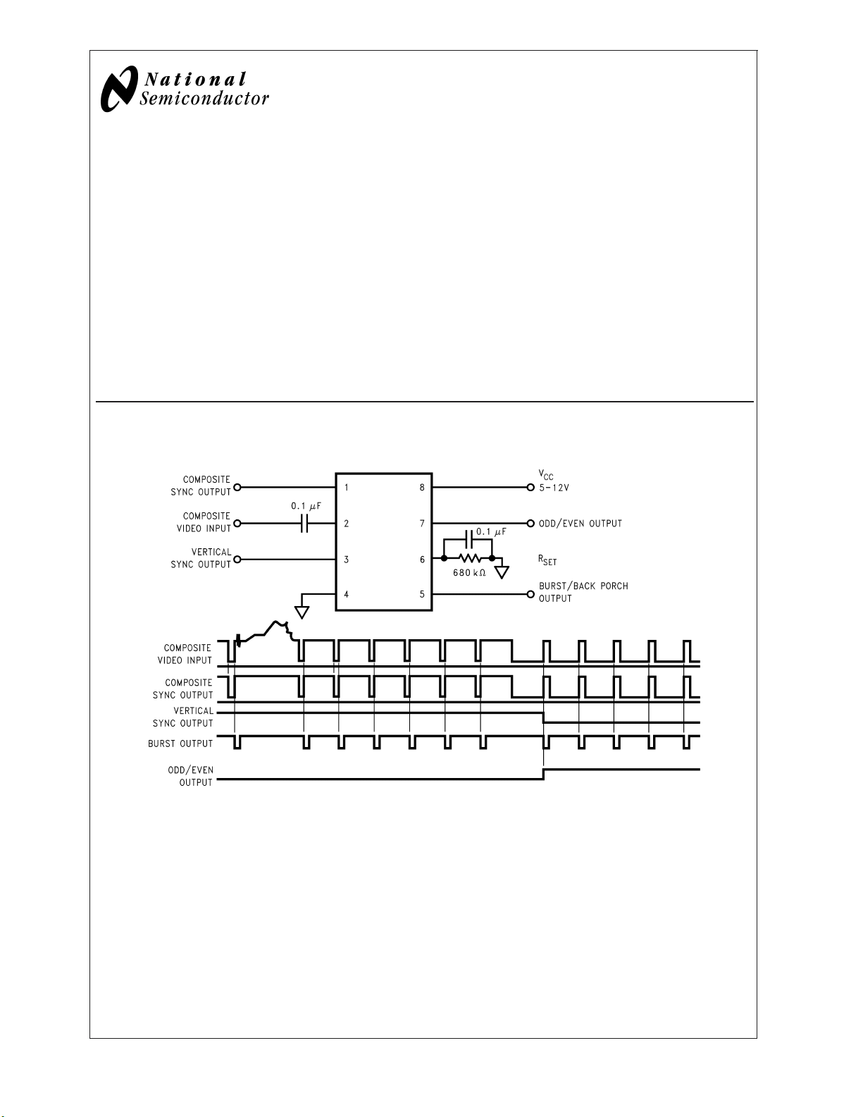
Connection Diagram
LM1881N
Features
n AC coupled composite input signal
>
n
10 kΩ input resistance
<
n
10 mA power supply drain current
n Composite sync and vertical outputs
n Odd/even field output
n Burst gate/back porch output
n Horizontal scan rates to 150 kHz
n Edge triggered vertical output
n Default triggered vertical output for non-standard video
signal (video games-home computers)
n -40˚C to +85˚C operation (LM1881-X)
Order Number LM1881M or LM1881N (0˚C to +70˚C)
Order Number LM1881M-X or LM1881N-X (-40˚C to +85˚C)
See NS Package Number M08A or N08E
*PAL in this datasheet refers to European broadcast TV standard “Phase Alternating Line”, and not to Programmable Array Logic.
© 2003 National Semiconductor Corporation DS009150 www.national.com
00915001
Page 2

Absolute Maximum Ratings (Note 1)
If Military/Aerospace specified devices are required,
please contact the National Semiconductor Sales Office/
Distributors for availability and specifications.
Supply Voltage 13.2V
Input Voltage 3 V
LM1881, LM1881-X
Output Sink Currents; Pins, 1, 3, 5 5 mA
6V
P-P(VCC
P-P(VCC
= 5V)
≥ 8V)
Package Dissipation (Note 2) 1100 mW
Storage Temperature Range −65˚C to +150˚C
ESD Susceptibility (Note 3) 2 kV
Soldering Information
Dual-In-Line Package (10 sec.) 260˚C
Small Outline Package
Vapor Phase (60 sec.) 215˚C
Infrared (15 sec.) 220˚C
Output Sink Current; Pin 7 2 mA
Electrical Characteristics LM1881
VCC= 5V; R
Parameter Conditions Min Typ (Note 4) Max Units
Supply Current Outputs at
DC Input Voltage Pin 2 1.3 1.5 1.8 V
Input Threshold Voltage (Note 5) 55 70 85 mV
Input Discharge Current Pin 2; V
Input Clamp Charge Current Pin 2; V
R
Pin Reference Voltage Pin 6; (Note 6) 1.10 1.22 1.35 V
SET
Composite Sync. & Vertical
Outputs
Burst Gate & Odd/Even
Outputs
Composite Sync. Output I
Vertical Sync. Output I
Burst Gate Output I
Odd/Even Output I
Vertical Sync Width 190 230 300 µs
Burst Gate Width 2.7 kΩ from Pin 5 to V
Vertical Default Time (Note 7) 32 65 90 µs
= 680 kΩ;TA= 0˚C to +70˚C by correlation with 100% electrical testing at TA=25˚C
SET
V
=5V
CC
Logic 1
= 2V 6 11 16 µA
IN
= 1V 0.2 0.8 mA
IN
I
=40µA;
OUT
Logic 1
I
= 1.6 mA
OUT
Logic 1
I
=40µA;
OUT
Logic 1
= −1.6 mA; Logic 0; Pin 1 0.2 0.8 V
OUT
= −1.6 mA; Logic 0; Pin 3 0.2 0.8 V
OUT
= −1.6 mA; Logic 0; Pin 5 0.2 0.8 V
OUT
= −1.6 mA; Logic 0; Pin 7 0.2 0.8 V
OUT
= 12V
V
CC
VCC=5V
= 12V
V
CC
VCC=5V
= 12V
V
CC
VCC=5V
= 12V
V
CC
CC
4.0
11.0
2.4
10.0
4.0
11.0
2.5 4 4.7 µs
5.2
5.5
4.5
3.6
4.5
10
12
mA
V
V
V
www.national.com 2
Page 3
Electrical Characteristics LM1881–X
VCC= 5V; R
Parameter Conditions Min Typ Max Units
Supply Current Outputs at
DC Input Voltage Pin 2 1.3 1.5 1.8 V
Input Threshold Voltage 55 70 85 mV
Input Discharge Current Pin 2; V
Input Clamp Charge Current Pin 2; V
R
Pin Reference Voltage Pin 6; 1.10 1.22 1.35 V
SET
Composite Sync. & Vertical
Outputs
Burst Gate & Odd/Even
Outputs
Composite Sync. Output I
Vertical Sync. Output I
Burst Gate Output I
Odd/Even Output I
Vertical Sync Width 140 230 588 µs
Burst Gate Width 2.7 kΩ from Pin 5 to V
Vertical Default Time 32 65 90 µs
Note 1: Absolute Maximum Ratings indicate limits beyond which damage to the device may occur. For guaranteed specifications and test conditions, see the
Electrical Characteristics. The guaranteed specifications apply only for the test conditions listed.
Note 2: For operation in ambient temperatures above 25˚C, the device must be derated based on a 150˚C maximum junction temperature and a package thermal
resistance of 110˚C/W, junction to ambient.
Note 3: ESD susceptibility test uses the “human body model, 100 pF discharged through a 1.5 kΩ resistor”.
Note 4: Typicals are at T
Note 5: Relative difference between the input clamp voltage and the minimum input voltage which produces a horizontal output pulse.
Note 6: Careful attention should be made to prevent parasitic capacitance coupling from any output pin (Pins 1, 3, 5 and 7) to the R
Note 7: Delay time between the start of vertical sync (at input) and the vertical output pulse.
= 680 kΩ;TA= –40˚C to +85˚C by correlation with 100% electrical testing at TA=25˚C
SET
V
=5V
CC
Logic 1
= 2V 6 11 16 µA
IN
= 1V 0.2 0.8 mA
IN
I
=40µA;
OUT
Logic 1
I
= 1.6 mA
OUT
Logic 1
I
=40µA;
OUT
Logic 1
= −1.6 mA; Logic 0; Pin 1 0.2 0.8 V
OUT
= −1.6 mA; Logic 0; Pin 3 0.2 0.8 V
OUT
= −1.6 mA; Logic 0; Pin 5 0.2 0.8 V
OUT
= −1.6 mA; Logic 0; Pin 7 0.2 0.8 V
OUT
= 25˚C and represent the most likely parametric norm.
J
= 12V
V
CC
VCC=5V
= 12V
V
CC
VCC=5V
= 12V
V
CC
VCC=5V
= 12V
V
CC
CC
4.0
11.0
2.4
10.0
4.0
11.0
2.2 4 4.7 µs
5.2
5.5
4.5
3.6
4.5
10
12
SET
mA
V
V
V
pin (Pin 6).
LM1881, LM1881-X
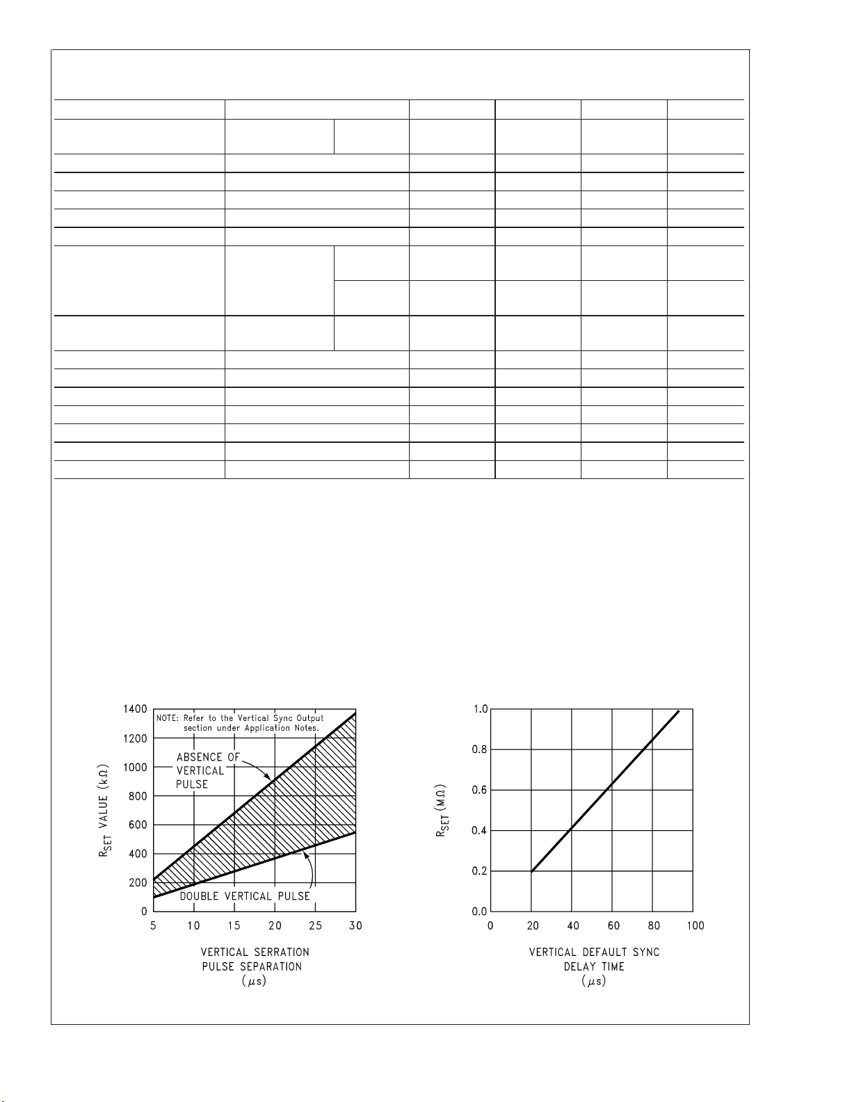
Typical Performance Characteristics
R
Value Selection
SET
vs Vertical Serration
Pulse Separation
00915007 00915008
Vertical Default
Sync Delay Time
vs R
SET
www.national.com3
Page 4
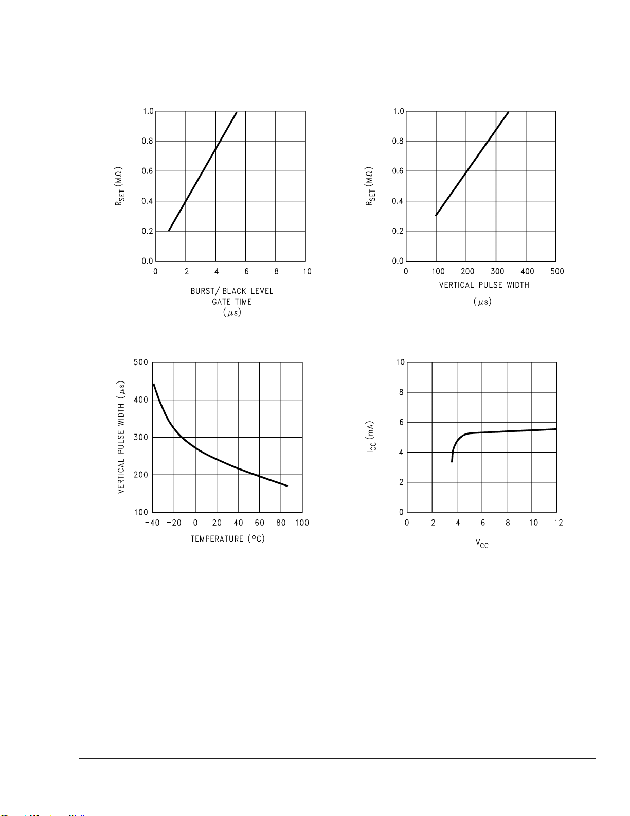
Typical Performance Characteristics (Continued)
LM1881, LM1881-X
Burst/Black Level
Gate Time vs R
SET
Vertical Pulse
Width vs Temperature
00915009
Vertical Pulse
Width vs R
SET
Supply Current vs
Supply Voltage
00915010
00915011
Application Notes
The LM1881 is designed to strip the synchronization signals
from composite video sources that are in, or similar to, the
N.T.S.C. format. Input signals with positive polarity video
(increasing signal voltage signifies increasing scene brightness) from 0.5V (p-p) to 2V (p-p) can be accommodated.
The LM1881 operates from a single supply voltage between
5V DC and 12V DC. The only required external components
besides a power supply decoupling capacitor at pin 8 and a
set current decoupling capacitor at pin 6, are the composite
input coupling capacitor at pin 2 and one resistor at pin 6 that
sets internal current levels. The resistor on pin 6 (i.e. R
allows the LM1881 to be adjusted for source signals with line
scan frequencies differing from 15.734 kHz. Four major sync
signals are available from the I/C; composite sync including
both horizontal and vertical scan timing information; a verti-
www.national.com 4
)
set
00915002
cal sync pulse; a burst gate or back porch clamp pulse; and
an odd/even output. The odd/even output level identifies
which video field of an interlaced video source is present at
the input. The outputs from the LM1881 can be used to
gen-lock video camera/VTR signals with graphics sources,
provide identification of video fields for memory storage,
recover suppressed or contaminated sync signals, and provide timing references for the extraction of coded or uncoded
data on specific video scan lines.
To better understand the LM1881 timing information and the
type of signals that are used, refer to Figure 1(a-e) which
shows a portion of the composite video signal from the end
of one field through the beginning of the next field.
Page 5

Application Notes (Continued)
COMPOSITE SYNC OUTPUT
The composite sync output, Figure 1(b), is simply a reproduction of the signal waveform below the composite video
black level, with the video completely removed. This is obtained by clamping the video signal sync tips to 1.5V DC at
Pin 2 and using a comparator threshold set just above this
voltage to strip the sync signal, which is then buffered out to
Pin 1. The threshold separation from the clamped sync tip is
nominally 70 mV which means that for the minimum input
level of 0.5V (p-p), the clipping level is close to the halfway
point on the sync pulse amplitude (shown by the dashed line
on Figure 1(a). This threshold separation is independent of
the signal amplitude, therefore, for a 2V (p-p) input the
clipping level occurs at 11% of the sync pulse amplitude. The
charging current for the input coupling capacitor is 0.8 mA,
Normally the signal source for the LM1881 is assumed to be
clean and relatively noise-free, but some sources may have
excessive video peaking, causing high frequency video and
chroma components to extend below the black level reference. Some video discs keep the chroma burst pulse
present throughout the vertical blanking period so that the
burst actually appears on the sync tips for three line periods
instead of at black level. A clean composite sync signal can
be generated from these sources by filtering the input signal.
When the source impedance is low, typically 75Ω, a 620Ω
resistor in series with the source and a 510 pF capacitor to
ground will form a low pass filter with a corner frequency of
500 kHz. This bandwidth is more than sufficient to pass the
sync pulse portion of the waveform; however, any subcarrier
content in the signal will be attenuated by almost 18 dB,
effectively taking it below the comparator threshold. Filtering
will also help if the source is contaminated with thermal
noise. The output waveforms will become delayed from between 40 ns to as much as 200 ns due to this filter. This
much delay will not usually be significant but it does contribute to the sync delay produced by any additional signal
processing. Since the original video may also undergo processing, the need for time delay correction will depend on
the total system, not just the sync stripper.
VERTICAL SYNC OUTPUT
A vertical sync output is derived by internally integrating the
composite sync waveform (Figure 2). To understand the
generation of the vertical sync pulse, refer to the lower left
hand section Figure 2. Note that there are two comparators
in the section. One comparator has an internally generated
voltage reference called V
other comparator has an internally generated voltage reference called V
going to one of its inputs. Both comparators
2
have a common input at their noninverting input coming from
the internal integrator. The internal integrator is used for
integrating the composite sync signal. This signal comes
from the input side of the composite sync buffer and are
positive going sync pulses. The capacitor to the integrator is
internal to the LM1881. The capacitor charge current is set
by the value of the external resistor R
integrator is going to be at a low voltage during the normal
horizontal lines because the integrator has a very short time
to charge the capacitor, which is during the horizontal sync
period. The equalization pulses will keep the output voltage
of the integrator at about the same level, below the V
During the vertical sync period the narrow going positive
pulses shown in Figure 1 is called the serration pulse. The
wide negative portion of the vertical sync period is called the
vertical sync pulse. At the start of the vertical sync period,
going to one of its inputs. The
1
. The output of the
SET
LM1881, LM1881-X
before the first Serration pulse occurs, the integrator now
charges the capacitor to a much higher voltage. At the first
serration pulse the integrator output should be between V
and V2. This would give a high level at the output of the
comparator with V
as one of its inputs. This high is clocked
1
into the “D” flip-flop by the falling edge of the serration pulse
(remember the sync signal is inverted in this section of the
LM1881). The “Q” output of the “D” flip-flop goes through the
OR gate, and sets the R/S flip-flop. The output of the R/S
flip-flop enables the internal oscillator and also clocks the
ODD/EVEN “D” flip-flop. The ODD/EVEN field pulse operation is covered in the next section. The output of the oscillator goes to a divide by 8 circuit, thus resetting the R/S
flip-flop after 8 cycles of the oscillator. The frequency of the
oscillator is established by the internal capacitor going to the
oscillator and the external R
. The “Q” output of the R/S
SET
flip-flop goes to pin 3 and is the actual vertical sync output of
the LM1881. By clocking the “D” flip-flop at the start of the
first serration pulse means that the vertical sync output pulse
starts at this point in time and lasts for eight cycles of the
internal oscillator as shown in Figure 1.
How R
affects the integrator and the internal oscillator is
SET
shown under the Typical Performance Characteristics. The
first graph is “R
Value Selection vs Vertical Serration
SET
Pulse Separation”. For this graph to be valid, the vertical
sync pulse should last for at least 85% of the horizontal half
line (47% of a full horizontal line). A vertical sync pulse from
any standard should meet this requirement; both NTSC and
PAL do meet this requirement (the serration pulse is the
remainder of the period, 10% to 15% of the horizontal half
line). Remember this pulse is a positive pulse at the integrator but negative in Figure 1. This graph shows how long it
takes the integrator to charge its internal capacitor above V
With R
be too small to charge the capacitor above V
too large the charging current of the integrator will
SET
, thus there will
1
be no vertical synch output pulse. As mentioned above, R
also sets the frequency of the internal oscillator. If the oscillator runs too fast its eight cycles will be shorter than the
vertical sync portion of the composite sync. Under this condition another vertical sync pulse can be generated on one of
the later serration pulse after the divide by 8 circuit resets the
R/S flip-flop. The first graph also shows the minimum R
necessary to prevent a double vertical pulse, assuming that
the serration pulses last for only three full horizontal line
periods (six serration pulses for NTSC). The actual pulse
width of the vertical sync pulse is shown in the “Vertical
Pulse Width vs R
” graph. Using NTSC as an example,
SET
lets see how these two graphs relate to each other. The
Horizontal line is 64 µs long, or 32 µs for a horizontal half
line. Now round this off to 30 µs. In the “R
Value Selection
SET
vs Vertical Serration Pulse Separation” graph the minimum
resistor value for 30 µs serration pulse separation is about
550 kΩ. Going to the “Vertical Pulse Width vs R
SET
one can see that 550 kΩ gives a vertical pulse width of about
180 µs, the total time for the vertical sync period of NTSC (3
horizontal lines). A 550 kΩ will set the internal oscillator to a
frequency such that eight cycles gives a time of 180 µs, just
long enough to prevent a double vertical sync pulse at the
vertical sync output of the LM1881.
The LM1881 also generates a default vertical sync pulse
when the vertical sync period is unusually long and has no
serration pulses. With a very long vertical sync time the
.
1
integrator has time to charge its internal capacitor above the
voltage level V
. Since there is no falling edge at the end of
2
a serration pulse to clock the “D” flip-flop, the only high signal
going to the OR gate is from the default comparator when
output of the integrator reaches V
. At this time the R/S
2
SET
SET
” graph
1
.
1
www.national.com5
Page 6

Application Notes (Continued)
flip-flop is toggled by the default comparator, starting the
vertical sync pulse at pin 3 of the LM1881. If the default
vertical sync period ends before the end of the input vertical
sync period, then the falling edge of the vertical sync (positive pulse at the “D” flip-flop) will clock the high output from
the comparator with V
LM1881, LM1881-X
ger the oscillator, generating a second vertical sync output
pulse. The “Vertical Default Sync Delay Time vs R
shows the relationship between the R
delay time from the start of the vertical sync period before
the default vertical sync pulse is generated. Using the NTSC
example again the smallest resistor for R
vertical default time delay is about 50 µs, much longer than
the 30 µs serration pulse spacing.
A common question is how can one calculate the required
with a video timing standard that has no serration
R
SET
pulses during the vertical blanking. If the default vertical sync
is to be used this is a very easy task. Use the “Vertical
Default Sync Delay Time vs R
essary R
to give the desired delay time for the vertical
SET
sync output signal. If a second pulse is undesirable, then
check the “Vertical Pulse Width vs R
as a reference input. This will retrig-
1
value and the
SET
is 500 kΩ. The
SET
” graph to select the nec-
SET
” graph to make sure
SET
SET
” graph
the vertical output pulse will extend beyond the end of the
input vertical sync period. In most systems the end of the
vertical sync period may be very accurate. In this case the
preferred design may be to start the vertical sync pulse at the
end of the vertical sync period, similar to starting the vertical
sync pulse after the first serration pulse. A VGA standard is
to be used as an example to show how this is done. In this
standard a horizontal line is 32 µs long. The vertical sync
period is two horizontal lines long, or 64 µs. The vertical
default sync delay time must be longer than the vertical
sync period of 64 µs. In this case R
680 kΩ.R
integrator to reach V
must still be small enough for the output of the
SET
before the end of the vertical period of
1
must be larger than
SET
the input pulse. The first graph can be used to confirm that
is small enough for the integrator. Instead of using the
R
SET
vertical serration pulse separation, use the actual pulse
width of the vertical sync period, or 64 µs in this example.
This graph is linear, meaning that a value as large as 2.7 MΩ
can be used for R
(twice the value as the maximum at
SET
30 µs). Due to leakage currents it is advisable to keep the
value of R
under 2.0 MΩ. In this example a value of 1.0
SET
MΩ is selected, well above the minimum of 680 kΩ. With this
value for R
the pulse width of the vertical sync output
SET
pulse of the LM1881 is about 340 µs.
FIGURE 1. (a) Composite Video; (b) Composite Sync; (c) Vertical Output Pulse;
(d) Odd/Even Field Index; (e) Burst Gate/Back Porch Clamp
www.national.com 6
00915003
Page 7

Application Notes (Continued)
LM1881, LM1881-X
*Components Optional, See Text
ODD/EVEN FIELD PULSE
An unusual feature of LM1881 is an output level from Pin 7
that identifies the video field present at the input to the
LM1881. This can be useful in frame memory storage applications or in extracting test signals that occur in alternate
fields. For a composite video signal that is interlaced, one of
the two fields that make up each video frame or picture must
have a half horizontal scan line period at the end of the
vertical scan — i.e., at the bottom of the picture. This is called
the “odd field” or “even field”. The “even field” or “field 2” has
a complete horizontal scan line at the end of the field. An odd
field starts on the leading edge of the first equalizing pulse,
whereas the even field starts on the leading edge of the
second equalizing pulse of the vertical retrace interval. Fig-
ure 1(a) shows the end of the even field and the start of the
odd field.
To detect the odd/even fields the LM1881 again integrates
the composite sync waveform (Figure 2). A capacitor is
charged during the period between sync pulses and discharged when the sync pulse is present. The period between
normal horizontal sync pulses is enough to allow the capacitor voltage to reach a threshold level of a comparator that
clears a flip-flop which is also being clocked by the sync
waveform. When the vertical interval is reached, the shorter
00915004
FIGURE 2.
integration time between equalizing pulses prevents this
threshold from being reached and the Q output of the flip-flop
is toggled with each equalizing pulse. Since the half line
period at the end of the odd field will have the same effect as
an equalizing pulse period, the Q output will have a different
polarity on successive fields. Thus by comparing the Q
polarity with the vertical output pulse, an odd/even field index
is generated. Pin 7 remains low during the even field and
high during the odd field.
BURST/BACKPORCH OUTPUT PULSE
In a composite video signal, the chroma burst is located on
the backporch of the horizontal blanking period. This period,
approximately 4.8 µs long, is also the black level reference
for the subsequent video scan line. The LM1881 generates a
pulse at Pin 5 that can be used either to retrieve the chroma
burst from the composite video signal (thus providing a
subcarrier synchronizing signal) or as a clamp for the DC
restoration of the video waveform. This output is obtained
simply by charging an internal capacitor starting on the
trailing edge of the horizontal sync pulses. Simultaneously
the output of Pin 5 is pulled low and held until the capacitor
charge circuit times out — 4 µs later. A shorter output burst
gate pulse can be derived by differentiating the burst output
www.national.com7
Page 8

Application Notes (Continued)
using a series C-R network. This may be necessary in
applications which require high horizontal scan rates in combination with normal (60 Hz–120 Hz) vertical scan rates.
APPLICATIONS
Apart from extracting a composite sync signal free of video
LM1881, LM1881-X
information, the LM1881 outputs allow a number of interesting applications to be developed. As mentioned above, the
burst gate/backporch clamp pulse allows DC restoration of
the original video waveform for display or remodulation on
an R.F. carrier, and retrieval of the color burst for color
synchronization and decoding into R.G.B. components. For
frame memory storage applications, the odd/even field lever
allows identification of the appropriate field ensuring the
correct read or write sequence. The vertical pulse output is
particularly useful since it begins at a precise time—the
rising edge of the first vertical serration in the sync waveform. This means that individual lines within the vertical
blanking period (or anywhere in the active scan line period)
can easily be extracted by counting the required number of
transitions in the composite sync waveform following the
start of the vertical output pulse.
The vertical blanking interval is proving popular as a means
to transmit data which will not appear on a normal T.V.
receiver screen. Data can be inserted beginning with line 10
(the first horizontal scan line on which the color burst appears) through to line 21. Usually lines 10 through 13 are not
used which leaves lines 14 through 21 for inserting signals,
which may be different from field to field. In the U.S., line 19
is normally reserved for a vertical interval reference signal
(VIRS) and line 21 is reserved for closed caption data for the
hearing impaired. The remaining lines are used in a number
of ways. Lines 17 and 18 are frequently used during studio
processing to add and delete vertical interval test signals
(VITS) while lines 14 through 18 and line 20 can be used for
Videotex/Teletext data. Several institutions are proposing to
transmit financial data on line 17 and cable systems use the
available lines in the vertical interval to send decoding data
for descrambler terminals.
Since the vertical output pulse from the LM1881 coincides
with the leading edge of the first vertical serration, sixteen
positive or negative transitions later will be the start of line 14
in either field. At this point simple counters can be used to
select the desired line(s) for insertion or deletion of data.
VIDEO LINE SELECTOR
The circuit in Figure 3 puts out a singe video line according
to the binary coded information applied to line select bits
b0–b7. A line is selected by adding two to the desired line
number, converting to a binary equivalent and applying the
result to the line select inputs. The falling edge of the
LM1881’s vertical pulse is used to load the appropriate
number into the counters (MM74C193N) and to set a start
count latch using two NAND gates. Composite sync transitions are counted using the borrow out of the desired number
of counters. The final borrow out pulse is used to turn on the
analog switch (CD4066BC) during the desired line. The falling edge of this signal also resets the start count latch,
thereby terminating the counting.
The circuit, as shown, will provide a single line output for
each field in an interlaced video system (television) or a
single line output in each frame for a non-interlaced video
system (computer monitor). When a particular line in only
one field of an interlaced video signal is desired, the odd/
even field index output must be used instead of the vertical
output pulse (invert the field index output to select the odd
field). A single counter is needed for selecting lines 3 to 14;
two counters are needed for selecting lines 15 to 253; and
three counters will work for up to 2046 lines. An output buffer
is required to drive low impedance loads.
MULTIPLE CONTIGUOUS VIDEO LINE
SELECTOR WITH BLACK LEVEL RESTORATION
The circuit in Figure 4 will select a number of adjoining lines
starting with the line selected as in the previous example.
Additional counters can be added as described previously
for either higher starting line numbers or an increased number of contiguous output lines. The back porch pulse output
of the LM1881 is used to gate the video input’s black level
through a low pass filter (10 kΩ, 10 µF) providing black level
restoration at the video output when the output selected
line(s) is not being gated through.
www.national.com 8
Page 9

Typical Applications
LM1881, LM1881-X
FIGURE 3. Video Line Selector
00915005
www.national.com9
Page 10
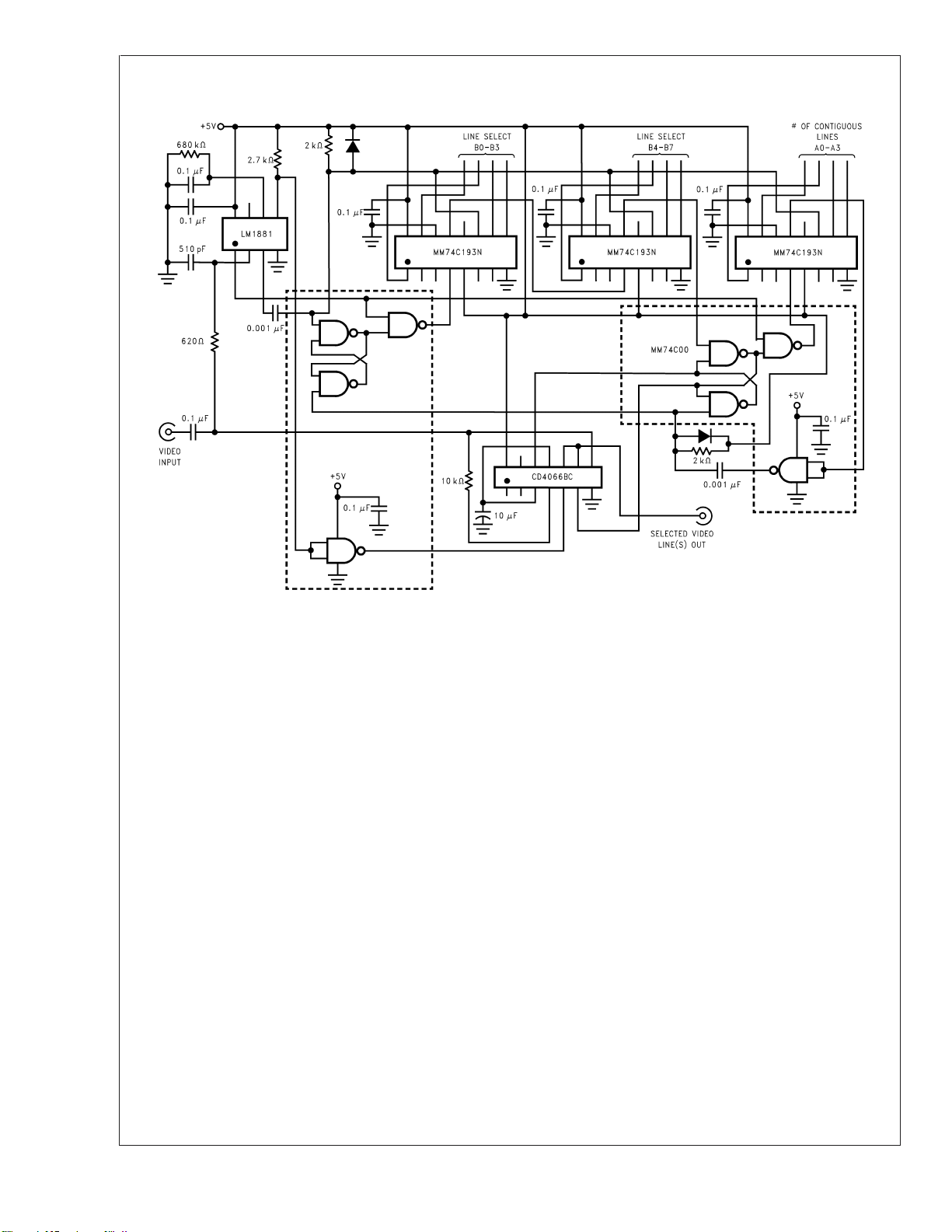
Typical Applications (Continued)
LM1881, LM1881-X
FIGURE 4. Multiple Contiguous Video Line Selector with Black Level Restoration
00915006
www.national.com 10
Page 11

Physical Dimensions inches (millimeters) unless otherwise noted
LM1881, LM1881-X
Molded Small Outline Package (M)
Order Number LM1881M (0˚C to +70˚C)
Order Number LM1881M-X (-40˚C to +85˚C)
NS Package Number M08A
Molded Dual-In-Line Package (N)
Order Number LM1881N (0˚C to +70˚C),
Order Number LM1881N-X (-40˚C to +85˚C)
NS Package Number N08E
www.national.com11
Page 12

LM1881, LM1881-X Video Sync Separator
Notes
LIFE SUPPORT POLICY
NATIONAL’S PRODUCTS ARE NOT AUTHORIZED FOR USE AS CRITICAL COMPONENTS IN LIFE SUPPORT
DEVICES OR SYSTEMS WITHOUT THE EXPRESS WRITTEN APPROVAL OF THE PRESIDENT AND GENERAL
COUNSEL OF NATIONAL SEMICONDUCTOR CORPORATION. As used herein:
1. Life support devices or systems are devices or
systems which, (a) are intended for surgical implant
into the body, or (b) support or sustain life, and
whose failure to perform when properly used in
accordance with instructions for use provided in the
2. A critical component is any component of a life
support device or system whose failure to perform
can be reasonably expected to cause the failure of
the life support device or system, or to affect its
safety or effectiveness.
labeling, can be reasonably expected to result in a
significant injury to the user.
National Semiconductor
Americas Customer
Support Center
Email: new.feedback@nsc.com
Tel: 1-800-272-9959
www.national.com
National does not assume any responsibility for use of any circuitry described, no circuit patent licenses are implied and National reserves the right at any time without notice to change said circuitry and specifications.
National Semiconductor
Europe Customer Support Center
Fax: +49 (0) 180-530 85 86
Email: europe.support@nsc.com
Deutsch Tel: +49 (0) 69 9508 6208
English Tel: +44 (0) 870 24 0 2171
Français Tel: +33 (0) 1 41 91 8790
National Semiconductor
Asia Pacific Customer
Support Center
Email: ap.support@nsc.com
National Semiconductor
Japan Customer Support Center
Fax: 81-3-5639-7507
Email: jpn.feedback@nsc.com
Tel: 81-3-5639-7560
 Loading...