

National Semiconductor LM1877 Technical data
现货库存、技术资料、百科信息、热点资讯,精彩尽在鼎好!
LM1877
Dual Audio Power Amplifier
General Description
The LM1877 is a monolithic dual power amplifier designed to
deliver 2W/channel continuous into8Ωloads.TheLM1877is
designed to operate with a low number of external components, and still provide flexibility for use in stereo phonographs, tape recorders and AM-FM stereo receivers, etc.
Each power amplifier is biased fromacommoninternalregulator to provide high power supply rejection, and output Q
point centering. The LM1877 is internally compensated for
all gains greater than 10.
Features
n 2W/channel
n −65 dB ripple rejection, output referred
n −65 dB channel separation, output referred
LM1877 Dual Audio Power Amplifier
February 1995
n Wide supply range, 6V–24V
n Very low cross-over distortion
n Low audio band noise
n AC short circuit protected
n Internal thermal shutdown
Applications
n Multi-channel audio systems
n Stereo phonographs
n Tape recorders and players
n AM-FM radio receivers
n Servo amplifiers
n Intercom systems
n Automotive products
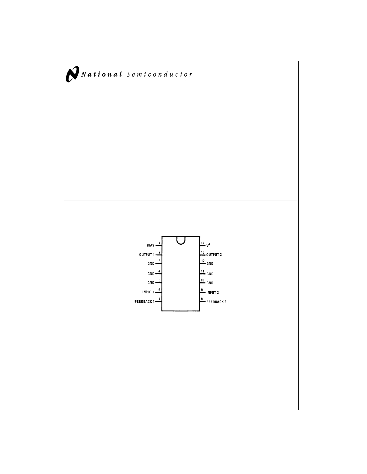
Connection Diagram
Dual-In-Line Package
or Surface Mount Package
DS007913-1
Top View
Order Number LM1877M-9 or LM1877N-9
See NS Package Number M14B or N14A
© 1999 National Semiconductor Corporation DS007913 www.national.com
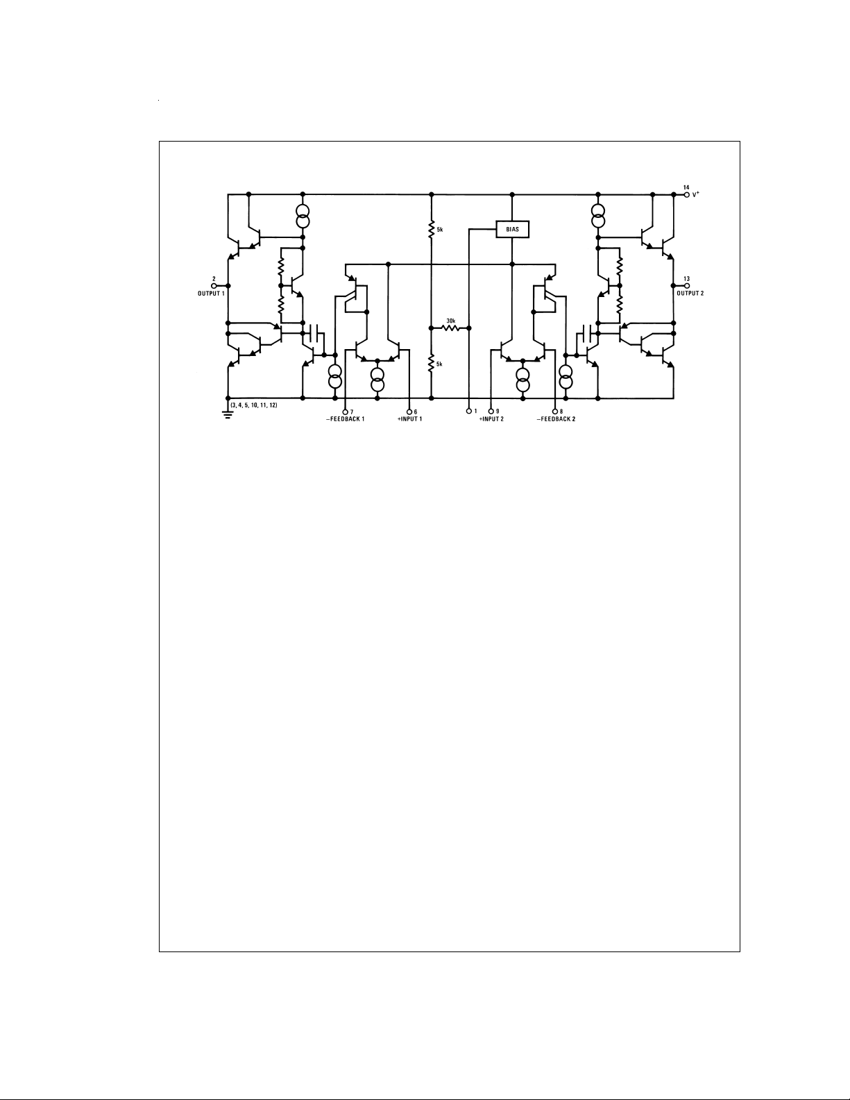
Equivalent Schematic Diagram
DS007913-2
www.national.com 2
Absolute Maximum Ratings (Note 1)
If Military/Aerospace specified devices are required,
please contact the National Semiconductor Sales Office/
Distributors for availability and specifications.
Supply Voltage 26V
Input Voltage
Operating Temperature 0˚C to +70˚C
Storage Temperature −65˚C to +150˚C
Junction Temperature 150˚C
±
0.7V
M-Package Infared (15 sec.) 220˚C
M-Package Vapor Phase (60 sec.) 215˚C
Thermal Resistance
(N-Package) 30˚C/W
θ
JC
(N-Package) 79˚C/W
θ
JA
(M-Package) 27˚C/W
θ
JC
(M-Package) 114˚C/W
θ
JA
Note 1: Absolute Maximum Ratings indicate limits beyond which damage to
the device may occur.Operating Ratings indicate conditions for which thedevice is functional, but do not guarantee specific performance limits.
Lead Temperature
N-Package Soldering (10 sec.) 260˚C
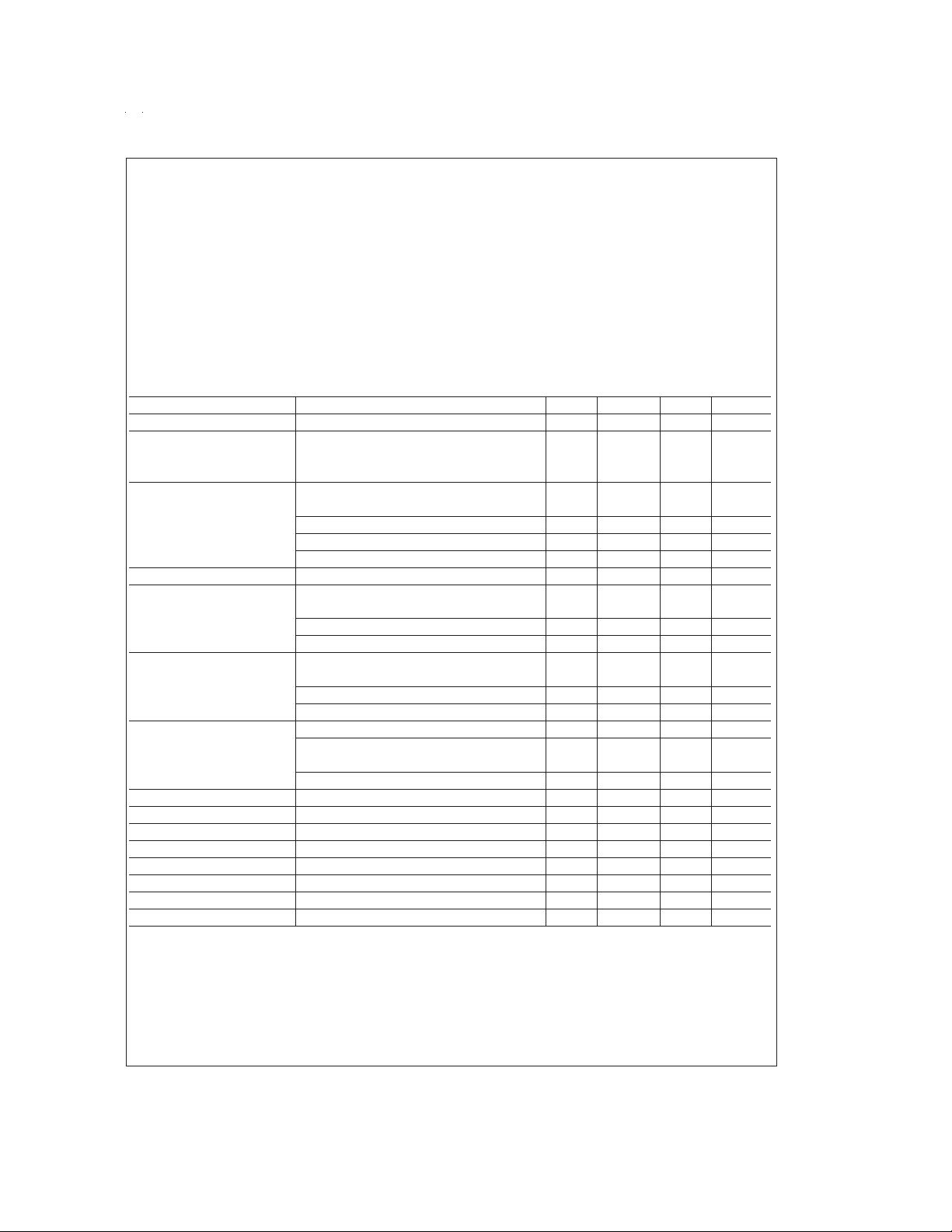
Electrical Characteristics
=
V
S
Total Supply Current P
Output Power THD=10
LM1877 V
Total Harmonic Distortion
LM1877 f=1 kHz, V
Output Swing R
Channel Separation C
PSRR Power Supply C
Rejection Ratio f=120 Hz, Output Referred
Noise Equivalent Input Noise
Open Loop Gain R
Input Offset Voltage 15 mV
Input Bias Current 50 nA
Input Impedance Open Loop 4 MΩ
DC Output Level V
Slew Rate 2.0 V/µs
Power Bandwidth 65 kHz
Current Limit 1.0 A
Note 2: For operation at ambient temperature greater than 25˚C, the LM1877 must be derated based on a maximum 150˚C junction temperature.
20V, T
=
25˚C, (Note 2) R
A
L
=
8Ω,A
=
50 (34 dB) unless otherwise specified
V
Parameter Conditions Min Typ Max Units
=
0W 25 50 mA
O
%
=
S
=
V
S
=
P
O
=
P
O
=
P
O
=
L
=
F
=
20V, R
12V, R
8Ω 2.0 W/Ch
L
=
8Ω 1.3 W/Ch
L
=
14V
S
50 mW/Channel 0.075
500 mW/Channel 0.045
1 W/Channel 0.055
8Ω V
50 µF, C
=
0.1 µF,
IN
S
−6 Vp-p
f=1 kHz, Output Referred
=
V
S
=
V
S
=
F
=
V
S
=
V
S
=
R
S
=
20V, V
7V, V
50 µF, C
20V, V
7V, V
0, C
4 Vrms −50 −70 dB
O
=
0.5 Vrms −60 dB
O
=
0.1 µF,
IN
=
1 Vrms −50 −65 dB
RIPPLE
=
0.5 Vrms −40 dB
RIPPLE
=
0.1 µF, 2.5 µV
IN
BW=20 Hz–20 kHz, Output Noise Wideband
=
R
S
S
S
=
0, C
0.1 µF, A
N
=
0, f=100 kHz, R
=
20V 9 10 11 V
200 0.80 mV
V
=
8Ω 70 dB
L
%
%
%
www.national.com3
 Loading...